1. Introduction
The rapid growth in the adoption of electric vehicles (EVs) is transforming transportation systems around the world [
1,
2,
3], This transformation is primarily driven by the urgent need to reduce greenhouse gas emissions, mitigate climate change, improve urban air quality, and decrease dependence on fossil fuels [
4,
5]. Governments and industry stakeholders have increasingly promoted electrification through regulatory frameworks, financial incentives, and investments in charging infrastructure [
6,
7]. As a result, EVs are emerging as a key pillar in the transition toward sustainable and low-carbon mobility systems [
8]. In parallel, continuous advances in battery technologies such as improvements in energy density, power capability, and cycle life have significantly increased vehicle driving range and overall performance [
9,
10,
11]. Despite these advances, the availability of efficient, reliable, and widely accessible charging infrastructure remains one of the most critical factors limiting the large-scale adoption of EVs [
12,
13]. Long charging times, limited range, and limited access to high-power charging stations continue to pose significant barriers to user acceptance and mass market penetration [
14,
15].
DC fast charging stations, commonly classified as Level 3 chargers, address this challenge by providing high power levels that enable fast charging times [
16,
17,
18]. However, the widespread deployment of these systems poses technical challenges related to conversion efficiency [
19,
20], energy management [
21], power density [
22], electromagnetic interference [
23], temperature [
24,
25] and the impact of high peak power demand on the electrical grid [
26]. As a result, the design of high-efficiency power conversion architecture has become a central research topic in power electronics for electromobility applications.
DC fast charging stations, commonly classified as Level 3 chargers, address this challenge by providing high levels of power, enabling rapid battery recharge in minutes rather than hours [
16,
27]. These fast-charging systems play a crucial role in supporting long-distance travel and commercial applications of electric vehicles [
28]. However, their widespread deployment poses several technical challenges, including high conversion losses [
29], limited power density [
30], electromagnetic interference (EMI) [
31], thermal management constraints [
24,
25], and the impact of high peak power demand on the electrical grid [
32]. Consequently, the development of high-efficiency, high-power-density, grid-compatible power conversion architectures has become an important focus of research in power electronics.
Recent studies have explored a wide range of DC-DC converter topologies for fast chargers for electric vehicles, including buck, boost, buck-boost, full-bridge, multilevel, and bidirectional isolated configurations. [
19,
33,
34,
35]. Among these, resonant converters, particularly the LLC topology, have attracted attention due to their soft switching characteristics, which reduce switching losses, improve efficiency at high switching frequencies, and mitigate electromagnetic interference [
22,
36,
37]. However, there are still differing opinions about its suitability for high-power fast charging, especially regarding control complexity, asymmetric efficiency, high switching losses, stress, and current ripple. [
38,
39,
40]. In contrast, multilevel and phase-shifted full-bridge converters offer robust power management, but often at the expense of increased component count and control complexity [
34,
41,
42].
In this context, this paper presents the design, simulation, and component selection for a Level 3 (DC) fast charger for electric vehicles based on an LLC resonant DC-DC converter using SiC power semiconductors. The main aim of this work is to demonstrate that LLC-based architecture can achieve high efficiency, reduce stress switching, and stable operation under fast charging conditions while maintaining a relatively simple and scalable design. Simulation results confirm that the proposed system meets the performance requirements of DC fast charging applications, supporting the conclusion that LLC resonant conversion is a viable and efficient solution for next-generation EV charging infrastructure.
The article is structured as follows:
Section 2 presents the mathematical analysis of the LLC resonant converter;
Section 3 presents the selection of SiC-based power semiconductor devices, the simulation results, and the integration of the battery with the results of level 3 fast charging.
Section 4 presents a discussion and comparison of what has been reported in the scientific literature, and finally,
Section 5 presents the conclusions of the article.
2. Mathematical Analysis of the LLC Resonant DC-DC Converter
To begin the mathematical analysis, the initial parameters shown in
Table 1 will be considered. These values are in accordance with Mexican standards applicable to fast charging infrastructure for electric vehicles, which establish minimum output values of 400 V and a nominal power of 50 kW for direct current charging systems [
43,
44,
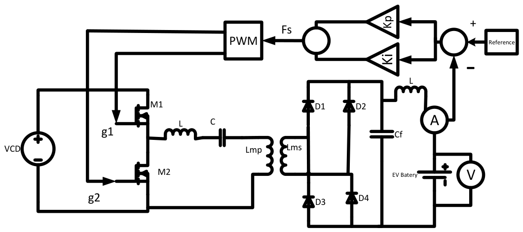
45]. The complete diagram of the resonant LLC charger, including the control stage, is shown in
Figure 1.
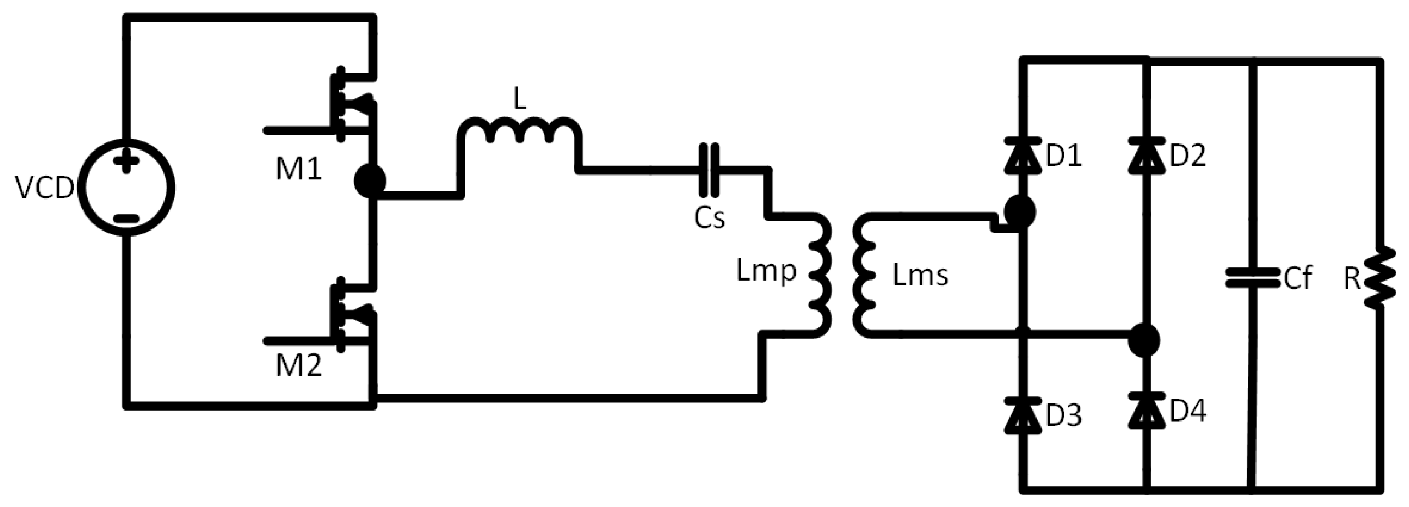
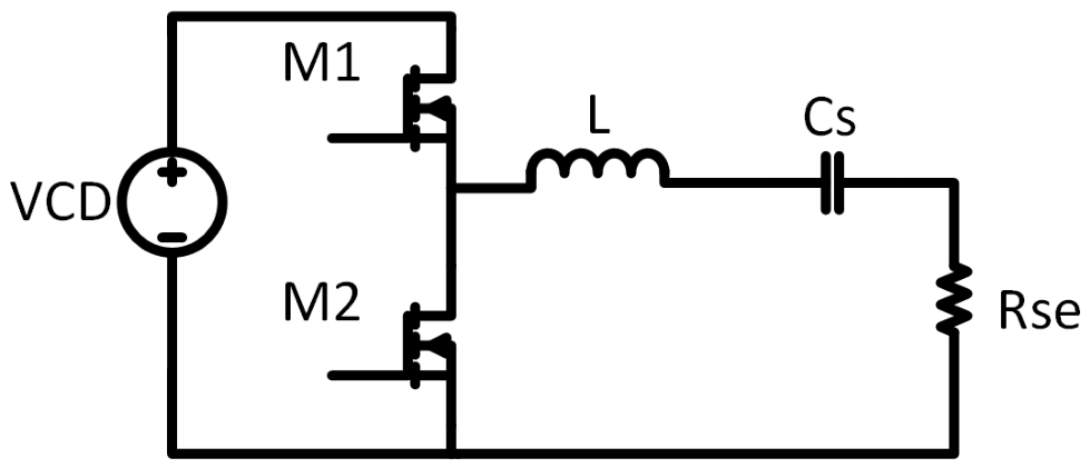
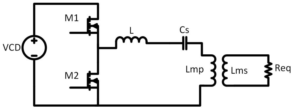
To simplify the calculations without involving the control stage and by modeling the electric vehicle’s battery as a resistive load, the diagram in
Figure 1 can be simplified to the diagram shown in
Figure 2.
Figure 1.
Resonant LLC Charger.
Figure 1.
Resonant LLC Charger.
Figure 2.
LLC resonant DC-DC converter.
Figure 2.
LLC resonant DC-DC converter.
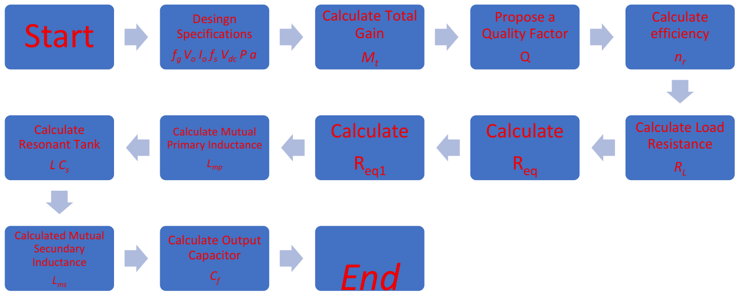
Before beginning the mathematical analysis, a diagram illustrates the step-by-step methodology used in the analysis. This diagram is shown in
Figure 3.
Table 1 shows the design specifications prior to beginning the mathematical analysis of the LLC resonant converter.
fg corresponds to the mains frequency in Mexico (60 Hz), Vo corresponds to the typical voltage of EV batteries, and the output current Io corresponds to the output of a Level 3 charger. Fs is selected for two reasons: it is a high frequency that SiC semiconductor devices can handle, and the inductive components remain small in both size and geometry due to the high frequency. The 800 V DC bus must be derived from a three-phase full-wave rectifier coupled to a DC-DC converter. It should be noted that this study does not include an EMI analysis; this would be appropriate for future work.
When working with resonant converters, it is essential to consider two main concepts: the angular switching frequency and the angular frequency of resonance . The switching angular frequency is determined by the operation of the power semiconductor devices, in this case the inverter MOSFETs, and defines the speed at which the converter’s switching processes are performed. On the other hand, the resonant angular frequency corresponds to the natural frequency of the resonant tank, formed by the interaction between the resonant inductor and the resonant capacitor, and is what allows the optimal operating conditions of the converter to be established.
For the LLC converter to operate in resonance mode, the switching frequency must match the resonance frequency (See Equations (1) and (2)). When this condition is met, the inductive and capacitive reactance’s of the resonant tank are equal in magnitude and cancel each other out, resulting in a predominantly resistive net impedance as seen from the inverter stage. This characteristic significantly reduces the phase shift between voltage and current.
To calculate the fundamental component of the power supply (
V1), the effective voltage is set in a DC bus component. This same component will help us establish the power values that will affect the MOSFETs. This is shown in Equation (3).
The system gain will be categorized into two different gains, the resonant tank gain (
M) and the complete system gain (
Mt). This is established because the
Vo is 450 V and the converter must function as a reducer, reducing from 800 V in the DC bus to 450 V. Equation (4), which is a function of a, is used to calculate
M.
Mt is the ratio between
Vo and
Vdc. This is shown in Equation (5).
To estimate the quality factor (
Q), the resonance condition establishes that
Q must be much greater than the minimum quality factor (
Qmin). This is shown in (6).
To calculate the minimum quality factor (
Qmin), substitute (4) into Equation (7).
Fulfilling the condition established in (6)
Q, it is proposed to be equal to Equation (8).
The quality factor is set to 5 because this value ensures that the resonant tank has high selectivity, low damping, and higher gain near the resonance frequency, while maintaining sufficient energy to ensure smooth switching in the MOSFETs.
The turns ratio of the resonant converter transformer is calculated by substituting
Mt and
M into Equation (9).
Substituting the values of (4) and (5) in Equation (9) gives (10).
Omitting losses in MOSFETs, considering losses in the full-wave bridge rectifier, and assuming that the diodes are Silicon Carbide (SiC), so that the forward voltage (
Vf) will be 1.5 V. Taking this data into account, the efficiency of the system is calculated using Equation (11).
The conduction losses in a MOSFET are given by Equation (12).
The current
IDS(rms) is approximately equal to Equation (13).
Calculating the conduction losses in the MOSFET would be equivalent to Equation (14).
With regard to mutual inductors, losses can be expressed in terms of the output voltage (
Votr), the turns ratio, the coupling factor (
k), and the input voltage (
Vitr), as shown in Equation (15).
Given that the MOSFETs switch alternately, this means that the maximum modulation voltage is +400 V and the minimum voltage is −400 V, resulting in a peak-to-peak voltage of 800 V, which is equivalent to the DC voltage value. Assuming perfect coupling the output voltage in transformed is show in Equation (16).
For the analysis of the electrical variables in the circuit, two reflected resistances must be calculated: the reflected resistance that will simulate a load around the full-wave bridge rectifier (
Req) and the load resistance that will be reflected in the LLC resonant tank
These reflected resistances are calculated using Equation (17) and. (18) The equivalent circuits of these two reflected resistances are shown in
Figure 3 and
Figure 4.
In an LLC converter, the equivalent resistance Req represents the combined effect of the rectifier, the output capacitor, and the resistive load. Although this system is nonlinear (due to the discontinuous conduction of the diodes and the filtering effect of the capacitor), the first-harmonic approximation (FHA) is used to model it as an equivalent linear load as seen by the resonant tank.
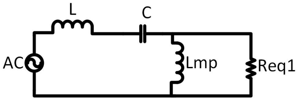
The circuit shown in
Figure 4 corresponds to the FHA equivalent model of an LLC converter as viewed from the primary side. In this model, the half-bridge of MOSFETs drives the resonant tank using a square-wave signal which, under the first-harmonic approximation, is considered an equivalent sinusoidal source.
The equivalent resistance
Req1 is calculated using Equation (19).
when using a transformer, it is essential to consider the system reactance
and magnetizing inductance (
Lmp).
is the opposition of inductive and capacitive elements to alternating current flow and is related to the operating frequency and inductance present in the circuit. High reactance can cause voltage drops and affect transformer efficiency. This reactance is calculated by substituting Equation (19) into (20).
Lmp measures the core’s capacity to store energy in the form of a magnetic field. It depends on the number of
n1 winding and the reluctance of the core. An adequate
Lmp ensures that the transformer operates efficiently without excessive losses or core saturation, which is key in high-power applications. This inductance is calculated using Equation (21).
The resistance reflected in the resonant tank (
Rse) determines how the load affects the dynamics of the resonant circuit. This resistance, seen from the primary winding of the transformer, is the result of the secondary winding load reflected through the winding transformation ratio. This resistance is calculated using Equation (24).
Figure 5 shows the equivalent circuit of
Rse.
The circuit shown in
Figure 5 represents the complete equivalent model of an LLC converter in the first-harmonic domain, where the contributions of the resonant tank and the transformer are clearly separated.
Rse represents the equivalent series resistance of the resonant tank.
To calculate the inductive and capacitive reactance’s required to achieve resonance, Equations (8) and (24) are substituted into Equation (25).
Equation (26) is used to calculate the inductive reactance that will be used to obtain the resonant tank inductor.
Equations (27) and (28) are used to calculate the capacitor (
Cs) and inductor (
L) of the resonant tank in the LLC converter.
To calculate the total reactance of the system (
Lms), Equation (21) is used and multiplied by the square of the value in Equation (10). This is shown in Equation (29).
As the capacitive and inductive reactance’s cancel each other out to establish the resonance condition, the current flows (
Ip) through
Rse and is calculated using Ohm’s law by dividing the fundamental voltage shown in (3) by
Rse shown in (24). The resulting value is shown in (30).
A detailed analysis of the calculation for this capacitor is available at [
46]. Since the MOSFETs switch alternately, each one receives the voltage
through the Drain and Source terminals, and this is calculated by dividing the value of (3) by 2. This is shown in Equation (33).
In each switching cycle, each MOSFET must withstand a drain current value. This current is calculated using Equation (34).
2.1. Thermal Model
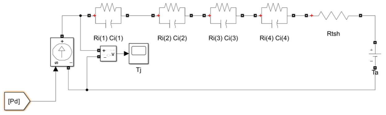
For the thermal analysis of the MOSFET, a four-branch Foster-type equivalent thermal network is used. The dynamic parameters of this network were taken directly from the PLECS model provided by the manufacturer, Infineon. This analytical representation is essential for modeling the transient behavior of heat flow from the semiconductor junction to the exterior. The values for the thermal resistors, the time constant, and the thermal capacitors are shown in
Table 2.
The junction temperature, denoted as
Tj, is determined based on a reference temperature
Tref (which typically corresponds to the ambient or heat sink temperature), the constant power dissipated by the device
Pd, and the transient thermal resistance
Zth(t). The primary relationship governing this behavior is given by Equation (35).
For a Foster topological network consisting of
n branches, the transient thermal impedance
Zth(
t) is mathematically defined as the sum of the exponential responses of each individual RC cell to the dissipated power. Its symbolic expression is given by Equation (36).
By fitting the mathematical model to Infineon specific parameters for a 4-branch network, we obtain the numerical equation that describes the time evolution of the junction temperature. Substituting the values of
Ri and
τi, the expression is given by Equation (37).
This analytical formulation allows for an accurate assessment of the semiconductor’s dynamic thermal behavior under different load profiles. The Foster thermal model is shown in
Figure 6.
Where
Tj is the junction temperature of the MOSFET and
Rtsh is the thermal resistance of the heat sink; this thermal resistance is calculated using Equation (38).
where
Tjmax is the maximum junction temperature specified in the manufacturer’s datasheet,
Tambmax is the maximum ambient temperature, and
is the average power dissipation (See
Figure 7).
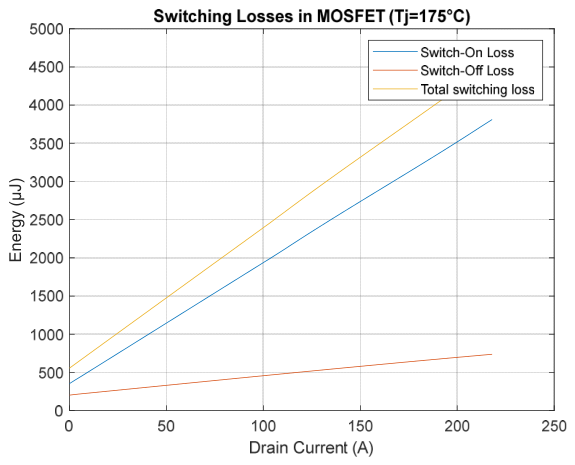
For the thermal analysis of the IMZA120R007M1H MOSFET, the switching power losses (
Eon and
Eoff) reported in the manufacturer’s datasheet have been incorporated into the simulation model. These losses, which are critical for determining temperature rise in high-frequency applications, are expressed in micro-Joules (µJ). These losses were implemented using a dynamic function dependent on the drain current (
ID), as shown in
Figure 8.
2.2. Selection of Semiconductor Devices and Passive Components
To ensure optimal performance of the proposed converter, a selection process for semiconductor devices and passive components was conducted based on electrical, thermal, and reliability criteria. This selection considers the system’s operating conditions, including voltage levels, current, switching frequency, and efficiency requirements. For the semiconductor devices, wide bandgap (WBG) technologies, such as SiC MOSFETs and diodes, were prioritized due to their advantages in terms of low switching losses, high power density, and the ability to operate at high temperatures. Key parameters considered in the selection include on-resistance RDSon, gate charge switching losses, as well as thermal characteristics associated with the packaging.
On the other hand, passive components were selected based on their ability to withstand the converter’s dynamic conditions, minimizing losses and ensuring operational stability. Inductors were sized considering ripple current and core saturation, while capacitors were selected based on their equivalent series resistance (ESR), ripple current handling capability, and thermal stability.
Table 3 provides a summary of selected semiconductor devices and passive components.
3. Results of Simulation
This section presents the selection of broadband semiconductor devices, the parameterization of the semiconductors to obtain an equivalent SPICE model, and the results obtained from the system simulation. The performance of the resonant converter is described, considering its steady-state operation, the quality of power transfer, and the interaction with the load. Finally, the analysis integrates the converter’s performance as a fast battery charger, evaluating its efficiency and operational consistency, which allows for verification that the proposed design meets the necessary conditions for safe and functional operation in electric vehicle applications.
Table 4 shows the configuration of the simulation model in Simulink (2024b)
Table 5 and
Table 6 show the selected semiconductor devices and their main electrical parameters.
Infineon® IMZA120R007M1H MOSFET, based on silicon carbide (SiC) technology, is a highly suitable choice for a resonant LLC converter designed to operate as a fast charger for electric vehicles. Its ability to withstand 1200 V of VDS provides sufficient safety margin for DC charging architectures with an 800 V bus, while its high current capabilities of 225 A in continuous conduction and up to 504 A in pulsed mode ensure robust operation against current peaks in the transient time.
From the point of view of conduction losses, the low RDS(on) value of 7 mΩ is particularly advantageous in LLC topologies, where the RMS current can be high. This parameter contributes directly to improving the overall efficiency of the system.
In terms of dynamic performance, the device’s parasitic capacitances make it particularly suitable for zero-voltage switching (ZVS) operation. The low reverse capacitance Crss of 61 pF minimizes the Miller effect, reducing losses during power-up transients, while a Coss of 420 pF promotes natural energy discharge through the resonant tank, an essential condition for maintaining ZVS over a wide range of loads and frequencies. This translates into lower switching losses, reduces stress on the driver.
Additionally, the use of SiC technology allows operation at high switching frequencies (500 KHz for this work) compared to Silicon (Si) devices, enabling a reduction in the size of the transformer and resonant elements, increasing the power density of the charger.
The Infineon® IDWD150G120C5 silicon carbide (SiC) diode is a robust and suitable technical choice for use in a full rectifier bridge at the output of a resonant LLC converter used as a fast charger for electric vehicles. Its 1200 V VRRM and DC blocking capability of the same level make it fully compatible with the high voltage levels present in EV chargers, providing ample safety margin against overvoltage’s and transients.
In terms of current capacity, the diode supports a continuous forward current of 343 A, ensuring reliable operation under the high output currents typical of fast chargers, as well as against the pulsating currents resulting from the rectification of high-frequency signals from the LLC’s resonant tank.
A particularly relevant feature is its low forward voltage of 1.5 V, characteristic of the latest generation of SiC diodes. This value significantly reduces conduction losses in the rectifier, directly impacting the overall system efficiency, a critical parameter in EV fast-charging applications where minimizing heat dissipation is essential.
In terms of dynamic behavior, the diode exhibits an IR current of 80 µA and a total capacitance of 600 pF, along with a total capacitive load of 660 nC. These characteristics are particularly advantageous in LLC topologies, as they reduce switching losses and electrical stress. Furthermore, being a SiC diode, it virtually eliminates the reverse recovery problem, improving the rectifier’s efficiency and reliability at high frequencies.
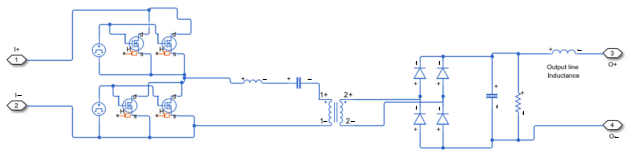
The design of the resonant LLC DC-DC converter is based on the specifications described in
Table 7. The schematic diagram created in Simulink
® is shown in
Figure 8.
3.1. Parasitic Elements in Passive Components
Prior to presenting the simulation results, a non-ideal model of the passive components was incorporated in order to accurately capture the dynamic behavior of the converter under actual operating conditions. In particular, the effects of parasitic elements were considered, as they have a significant impact on losses, transient response, and system stability.
Table 8 summarizes the values of the parasitic elements considered in the simulation, which were obtained from the manufacturers’ data sheets. The series resistance of the capacitors is calculated based on the dissipation factor
and the switching frequency, as shown in Equation (39).
3.2. Performance of the LLC Resonant Converter
The analysis of the resonant converter’s results details its dynamic behavior and energy conversion efficiency. These converters operate through resonance between inductors and capacitors, which facilitates a notable reduction in switching losses and optimizes the quality of energy transfer. In fast charging scenarios and high-power density electrical systems, resonant converters offer notable advantages in terms of efficiency, galvanic isolation, and the ability to maintain stable control even in the face of variations in load or input bus voltage. This section examines the most relevant electrical parameters, their behavior in transient and steady-state conditions, and the interaction between the resonant elements and the transformer, with the aim of evaluating the overall performance of the converter and its suitability for conversion applications in battery charging systems.
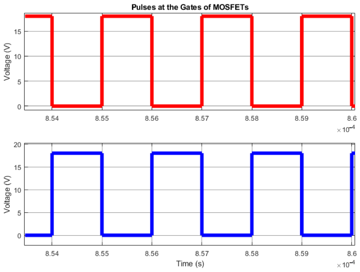
Figure 9 shows the analysis of the programmed behavior for the converter switching. The voltage applied to the gate, V
G, is set between 0 and 18 V, using a 50% duty cycle and a switching frequency of 500 kHz, to ensure high-frequency operation in the resonant tank. During this process, the control signal undergoes a programmed inversion, which is necessary to ensure correct excitation of the converter and maintain symmetry in the switching stage.
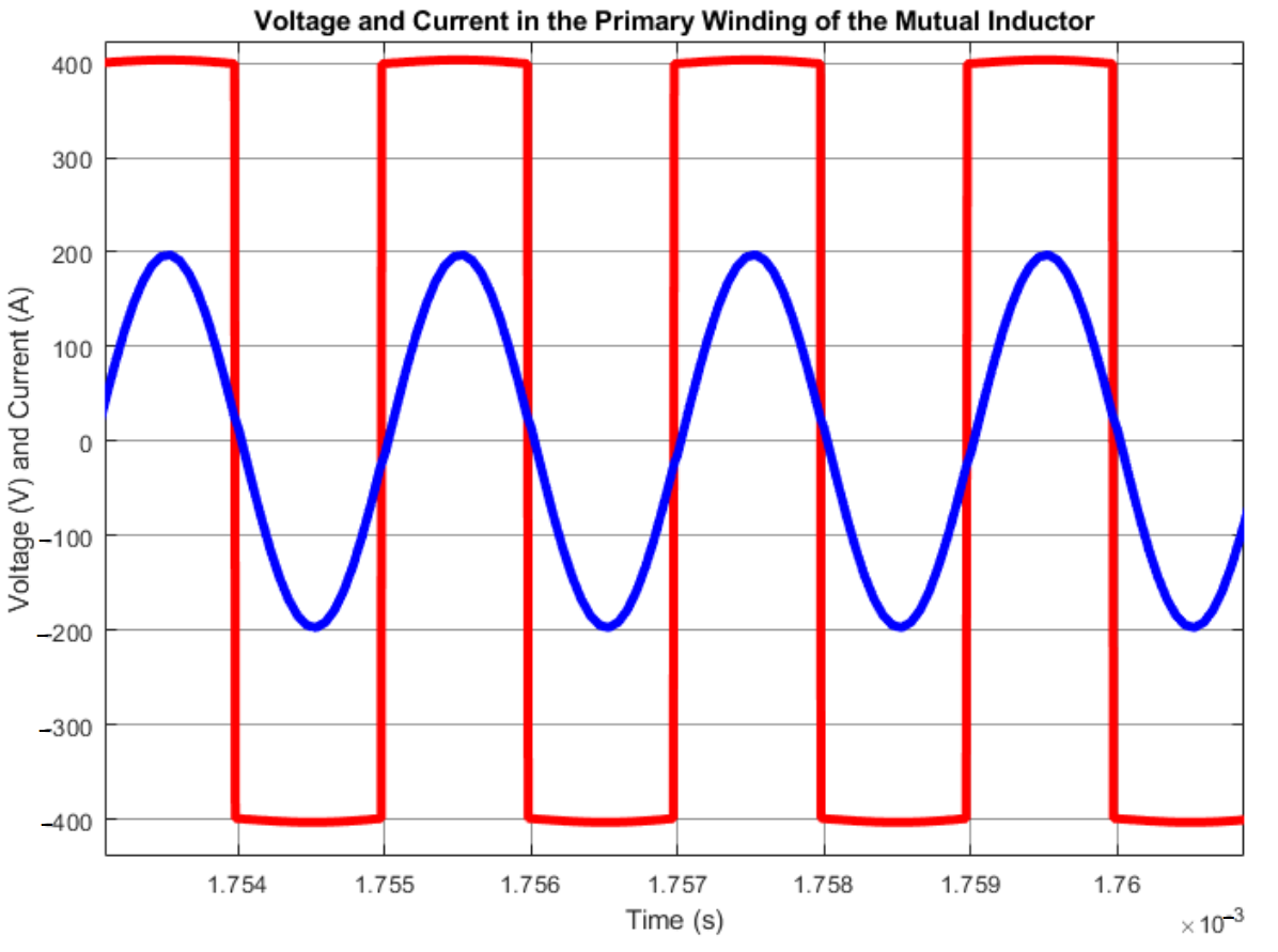
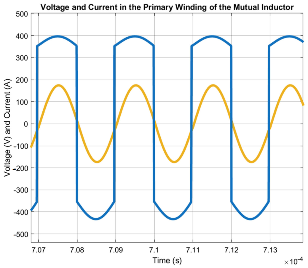
The converter’s supply voltage comes from the DC bus, where the 800 volts undergo an inversion process caused by the MOSFETs. On the other hand, the current is purely sinusoidal at a frequency of 500 KHz equal to the switching frequency, thanks to the resonance condition with a maximum amplitude of approximately 200 A, since each MOSFET conducts approximately 100 A (See Equation (34)) per half cycle and each pair of MOSFETs are in parallel (See
Figure 8), so the currents add up and this is the peak amplitude of the sinusoidal current. All this is shown in
Figure 10.
When considering the parasitic elements shown in
Table 8, the switching losses in the MOSFETs (see
Figure 7), and a magnetic coupling coefficient less than 1 (See Equation (15)), the simulation results for the voltage and current in the primary winding of the mutual inductor are shown in
Figure 11 and
Figure 12. The resonant current (mustard-colored sinusoidal signal) is less than 200 A peak; this is due to the losses already accounted for in the simulation.
Figure 12.
Voltage and Current in the Primary Winding of the Mutual Inductor (Considering losses).
Figure 12.
Voltage and Current in the Primary Winding of the Mutual Inductor (Considering losses).
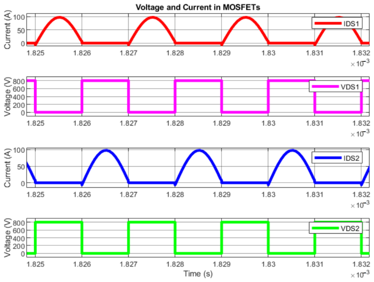
The drain-to-source current (I
DS) and drain-to-source voltage (V
DS) of two MOSFETs are shown in
Figure 11. These signals are complementary, as they would be the signals of MOSFET 1 (M
1) and MOSFET 2 (M
2) (See
Figure 2). Considering that M1 is composed of two MOSFETs in parallel, as is M2. Only one MOSFET from M1 and one MOSFET from M2 are plotted. Each MOSFET supports 800 V in V
DS corresponding to the DC bus level, and for the current in each complementary MOSFET, they conduct one half-cycle of the sinusoidal resonant current signal.
Considering switching and conduction losses in the MOSFETs (See
Figure 7),
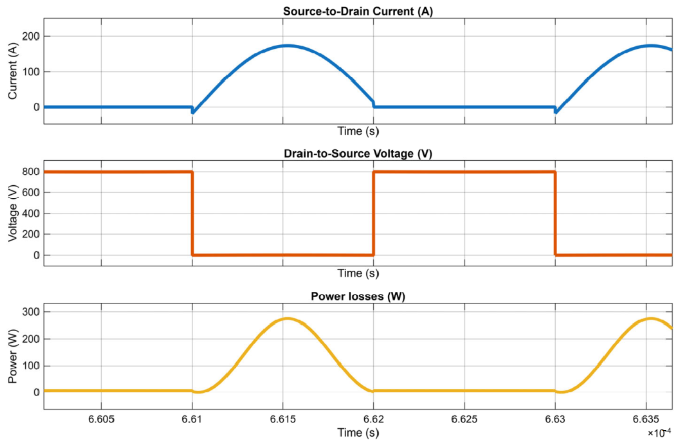
Figure 13 and
Figure 14 shows the simulation results for the VDS voltage and the IDS current. The voltage
VDS (top graph) oscillates at the resonance frequency between 800 V (DC bus level) and 1.62 V, which corresponds to the forward voltage of the SiC body diode incorporated into the MOSFET. The current
IDS (middle graph) oscillates between 174.5 A and 0.008 A at the resonance frequency. These voltage and current oscillations cause conduction losses in the MOSFETs (bottom graph) with a peak of 275 W per switching cycle; switching losses are minimal because the MOSFETs use soft switching due to the resonant condition.
The output signals of the LLC resonant converter are shown in
Figure 15. The output power is 48.69 kW, which implies a level 3 power transfer. The theoretical power is 50 kW, which consists of fast charging applications for EVs. The output voltage signal is 444 V, and the theoretical value is 450 V. For the output current signal, the value measured in the simulation was 109 A, and the theoretical current is 111 A. These results validate the LLC resonant converter, achieving an efficiency of 97.38%.
Figure 13.
Current and voltage signals in two MOSFETs.
Figure 13.
Current and voltage signals in two MOSFETs.
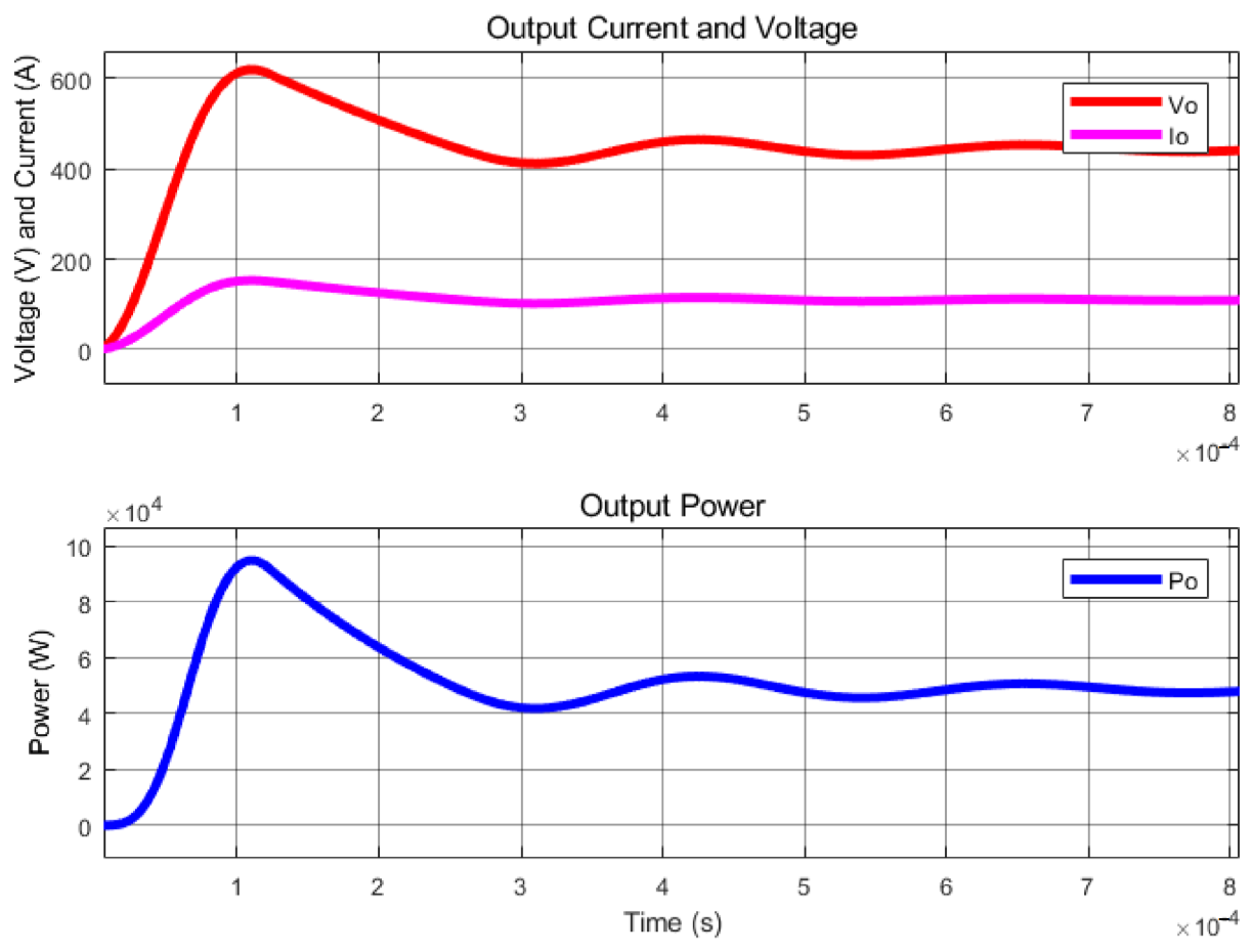
We consider all parasitic elements in the passive components shown in
Table 8, the conduction losses in the MOSFETs (See
Figure 7), imperfect magnetic coupling in the mutual inductors, and the conduction characteristics of the SiC diodes (see
Table 6). The output signals of the LLC resonant converter are shown in
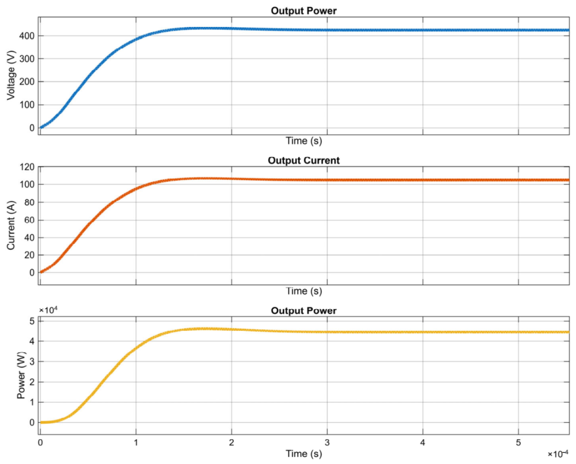
Figure 16. The output power is 41.98423 kW; the theoretical power is 50 kW, which enables fast-charging applications for electric vehicles. The output voltage signal is 419.84 V, and the theoretical value is 450 V. As for the output current signal, the value measured in the simulation was 103.66 A, and the theoretical current is 111.11 A. With these results, the LLC resonant converter achieves an efficiency of 83.96%. This efficiency is due to the high power (Level 3 in EV chargers), associated parasitic elements, conduction and switching losses, and imperfect magnetic coupling.
Figure 14.
Current and voltage signals in MOSFETs (considering losses).
Figure 14.
Current and voltage signals in MOSFETs (considering losses).
Figure 15.
Output voltage and current in the resonant converter.
Figure 15.
Output voltage and current in the resonant converter.
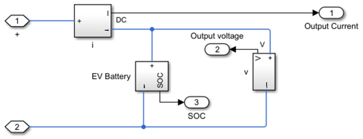
As part of the process of reviewing and validating the results, a battery was modeled with the aim of obtaining a functional representation of its state of charge (SoC) and the electrical parameters characteristic of a real battery. A battery with high energy density must be chosen, with a load capacity capable of withstanding 111 A continuous and with thermal stability, in addition to having a reliable Battery Management System (BMS). The block representation of the battery is shown in
Figure 17 and its parameters are shown in
Table 9.
Figure 16.
Output voltage and current in the resonant converter (considering all losses).
Figure 16.
Output voltage and current in the resonant converter (considering all losses).
Figure 17.
Battery blocks in Simulink.
Figure 17.
Battery blocks in Simulink.
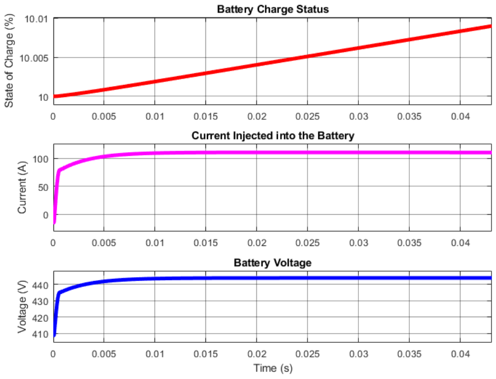
Once the resonant converter configuration is complete, the next step is to represent and analyze the system output variables with the integrated battery. This analysis allows the actual behavior of the charger to be evaluated under the established operating conditions, verifying that the voltage, current, and power levels comply with the parameters specified in the design. The representation of these variables is essential to validate the charger’s performance and ensure that it operates properly and reliably for fast charging applications. The results of this simulation are shown in
Figure 14. It is worth noting that, although all losses are already accounted for in the simulation model, the controller can be used to obtain the voltage, current, and power required by the electric vehicle’s battery. This can be addressed by increasing the DC level, and this function would be implemented in the controller.
Figure 18 shows the dynamic response of the fast-charging system based on an LLC resonant converter connected to the battery of an electric vehicle. The battery state of charge (SoC) graph reflects a small but continuous increase, consistent with a short simulation interval. This behavior is consistent with the charging curve of batteries in fast charging applications. The charging current is constant, which translates to the direct current (CC) state of charge in the battery. Overall, the results validate the stable operation of the resonant converter.
Figure 18.
Battery performance when charging.
Figure 18.
Battery performance when charging.






 ,
,