


Abstract
Accurate and efficient defect detection in printed circuit boards (PCBs) is critical for manufacturing quality control. Existing methods predominantly rely on manually extracted features such as surface texture, color, and shape for defect recognition and classification within small-dimensional feature datasets. A convolutional neural network (CNN) model was developed via transfer learning. Feature extraction involves diverse operations across different CNN layers. Essential features were selected, and dimensionality was reduced via either t-distributed stochastic neighbor embedding (t-SNE) or principal component analysis (PCA). Defect classification was subsequently performed by clustering the reduced features with either the K-means or K-nearest neighbors (KNN) algorithm. Compared with alternative model feature learning classifiers, the proposed small-dimensional CNN model performs significantly better. A defect recognition accuracy of 97.33% was achieved, with processing completed in approximately 60 s. This approach, which integrates transfer learning-based CNN feature extraction with dimensionality reduction and clustering techniques, provides a fast and effective method for high-precision defect detection and classification in PCBs.
1. Introduction
Electronic devices are fundamental to modern society, driving progress in the global electronics industry. Printed circuit boards (PCBs) serve as critical components within these devices, providing the essential interconnections for electronic elements across a vast array of circuits and products. Consequently, the design, manufacturing quality, and reliability of PCBs directly impact the performance and cost-effectiveness of electronic goods, making PCB research a priority in electronic engineering.
The evolution of electronic products imposes increasing demands on PCBs, including requirements for high density, high speed, high frequency, low power consumption, cost reduction, and environmental compliance. Meeting these challenges necessitates continuous refinement in PCB design, materials, manufacturing processes, and, crucially, testing protocols. Automated, high-precision defect detection is vital for ensuring quality and reliability across diverse applications, from consumer electronics to wearable devices, flexible electronics, and biomedical engineering.
While image recognition technology offers significant potential advantages for PCB defect detection—including efficiency, accuracy, reliability, automation, and scalability—traditional methods often remain labor intensive, time consuming, and susceptible to inconsistencies arising from environmental factors, operator skill, and fatigue. Convolutional neural networks (CNNs) represent a powerful tool for automated visual inspection. However, achieving high accuracy typically requires extensive training datasets and effective feature selection.
This study addresses these challenges by proposing a novel approach that leverages transfer learning. Features are extracted from input PCB defect images via established pretrained CNN models (including AlexNet, GoogleNet, ResNet50, and MobileNet). To overcome the dimensionality and data volume challenges, essential features are screened and reduced via dimensionality reduction techniques such as principal component analysis (PCA) or t-distributed stochastic neighbor embedding (t-SNE). The reduced feature set is then classified by clustering algorithms (K-means or K-nearest neighbors). This methodology focuses on identifying cluster centers within the training data, grouping similar data points, and utilizing image labels to enable rapid defect classification. The approach significantly reduces the volume of training data required by constructing a smaller, task-specific dataset for PCB defect detection. Comparative analysis demonstrated that, compared with conventional CNN feature learning classifiers, this method enhances both accuracy and efficiency in PCB defect analysis.
The key contribution of this study is introducing a novel hybrid framework that integrates transfer learning-based CNN feature extraction with subsequent dimensionality reduction and clustering, it presents a streamlined alternative to data-intensive deep learning models. This methodology is demonstrated to be highly effective, achieving a defect recognition accuracy of 97.33% with a complete processing time of approximately 60 s, thereby balancing high precision with practical efficiency. Ultimately, the work provides a robust and readily implementable solution that addresses the critical need for fast, reliable, and scalable quality control in electronics manufacturing.
2. Related Work
2.1. Image Feature Extraction
Image feature extraction is a fundamental process for obtaining meaningful information from visual data, enabling subsequent analysis across diverse applications, including facial recognition, object detection, and medical image analysis [1,2]. This process transforms raw pixel data into representations that capture essential characteristics such as shape, color, texture, and spatial relationships.
Within PCB manufacturing, precise feature extraction is critical for automatic optical inspection (AOI) systems tasked with identifying defects [3]. The intricate nature of PCB production processes inevitably leads to diverse defect phenomena, including variations in solder joints and component characteristics even within the same batch. Effective feature extraction provides the descriptive foundation necessary for reliable defect detection and classification.
Image feature extraction typically involves sequential steps:
- (1)
- Preprocessing: Enhancing raw images through noise reduction, contrast adjustment, and geometric correction to improve quality and reduce artifacts.
- (2)
- Segmentation: The image is partitioned into meaningful regions or objects for focused analysis.
- (3)
- Feature Extraction: Computing numerical or symbolic descriptors that represent key attributes (e.g., shape, color, texture, position) of the segmented regions.
- (4)
- Feature Selection: Identifying the most discriminative and relevant features to reduce the dimensionality and computational load.
- (5)
- Feature Matching: Comparing extracted features against reference templates or models to determine object identity or defect status.
Depending on specific application requirements, various methods and techniques can be employed for image feature extraction. In the context of PCB image analysis, common approaches include the following:
- (1)
- Color-based methods: Leveraging color differences between components and circuits via RGB/HSV color spaces or gray-level histograms.
- (2)
- Shape-based methods: Utilize geometric characteristics via edge detection, contour tracing, or Hough transforms.
- (3)
- Texture-based methods: Analysing surface patterns via gray-level co-occurrence matrices (GLCMs), wavelet transforms, or Gabor filters.
- (4)
- Deep Learning-Based Techniques: Employing artificial neural networks (ANNs) and CNNs to acquire feature representations autonomously from PCB components and circuits for tasks such as image classification and object detection. Strategies such as leveraging large datasets, utilizing pretrained networks, and fine-tuning are commonly employed to optimize performance [4].
2.2. PCB Defect Detection
Defect detection is a critical component of PCB manufacturing and is essential for ensuring product quality and reliability. AOI systems target various defects, including missing holes, mouse bites, open circuits, short circuits, burrs, and pseudo copper, by extracting pertinent information from PCB images for analysis.
Traditional defect detection methods, which rely on manual visual inspection or contact-based techniques, are often hampered by low efficiency, subjectivity, and susceptibility to interference. This has driven significant academic and industrial interest in deep learning-based approaches. These methods leverage large datasets of PCB images to train deep neural network models, enabling automatic learning of effective feature representations for efficient defect classification or localization.
PCB defect detection methodologies can be broadly categorized as follows:
Image Processing & Traditional Machine Learning-Based Methods: These techniques employ algorithms such as principal component analysis (PCA), Fourier transform, wavelet transform, and image pattern matching to extract features from PCB images. Defect detection and classification are subsequently performed by matching extracted features against predefined templates. A key limitation of these template-matching approaches is their sensitivity to variations in component position and lighting conditions, which can restrict robustness in complex industrial environments.
Deep Learning-Based Methods: Capitalizing on advances in CNNs, these approaches have demonstrated substantial success in PCB inspection. Compared with traditional techniques, Wei et al. [5] achieved high classification accuracy via a CNN-based reference comparison method, reporting superior performance and stability. Ling and Isa [6] provided a comprehensive survey analysing integrated approaches combining image processing, machine learning, and deep learning, detailing algorithms, procedures, metrics, and limitations. Lim et al. [7] developed a deep context learning-based detection model that incorporates an anomalous trend alarm system. Zheng et al. [8] proposed an improved fully convolutional network method, reporting significant enhancements in classification accuracy. Althubiti et al. [9] employed a VGG16 CNN architecture with optimizer tuning and learning rate adjustments, achieving 97.01% validation accuracy for defect classification on their dataset.
Physics-Informed & Multi-Modal AI Methods: Beyond visual pattern analysis, a growing research frontier focuses on integrating physical models and multi-sensor data with AI to diagnose functional and latent defects. For instance, in the domain of reliability monitoring, studies have combined finite element simulation of thermal stress with infrared thermography and deep learning to localize and classify thermal anomalies in PCBs under operational conditions [10]. These hybrid methods leverage physics-based constraints to enhance the interpretability and robustness of AI diagnostics, particularly for defects related to performance degradation rather than mere visual irregularities. While such approaches are powerful for functional failure analysis, they typically address a different problem scope—often post-assembly and under active stress—compared to the high-speed optical inspection of macroscopic manufacturing defects targeted in this study. The two paradigms can be viewed as complementary within a comprehensive PCB quality assurance pipeline.
2.3. Deep Learning
Deep learning represents a powerful paradigm for automatically extracting hierarchical features and knowledge from extensive datasets, enabling breakthroughs in complex tasks such as image recognition, speech recognition, and natural language processing [11,12,13]. This capability has driven significant advancements in automated visual inspection, including PCB defect detection.
The deep learning methodologies applied for PCB defect detection include the following:
- (1)
- CNN-based methods: CNNs, with their hierarchical structure of convolutional and pooling layers, effectively extract local and global features while maintaining translation and scale invariance. CNNs are widely used for PCB defect image classification [14] and bounding box regression for defect localization [15].
- (2)
- Region Proposal Network (RPN)-based Methods: RPNs, integrated within object detection frameworks, simultaneously generate candidate object regions and corresponding scores. These are refined by subsequent classifiers or regressors for precise localization, making them suitable for proposing and localizing defect regions in PCB images [16].
- (3)
- Fully Convolutional Network (FCN)-Based Methods: FCNs perform pixelwise semantic segmentation, assigning each pixel to a specific category. This fine-grained approach excels in tasks requiring detailed defect analysis, such as semantic segmentation and classification of PCB defect images [17].
The evolution of deep learning over the past decade, particularly the dominance of CNNs, has substantially enhanced image classification performance across diverse domains. Within PCB inspection, the YOLO-v5 model has demonstrated efficiency, accuracy, and high speed for defect detection [18]. Additionally, various deep learning methods have achieved high accuracy on multiple PCB defect datasets [19]. Deep learning models have been successfully applied to predict complex material properties, such as the in situ elastic modulus of PCB conductive layers, achieving high prediction accuracy (absolute error <3% for 99% of the validation modes) compared with finite element analysis [20]. The algorithms that achieve high accuracy (~95%) with rapid detection times (e.g., 0.027 s per image) meet stringent industrial requirements [17]. Such approaches can reduce memory demands while enhancing computational efficiency. A key strength of deep learning lies in its ability to leverage pretrained CNN models. These models, trained on massive datasets (e.g., ImageNet), embed rich, general feature representations and domain-specific knowledge [21,22,23]. Transfer learning exploits this knowledge, enabling effective feature extraction even for specific tasks with relatively limited training data [24]. This technique is particularly valuable for PCB defect detection, where the acquisition of large labelled datasets can be challenging. By using transfer learning on a pretrained CNN, essential features can be extracted from a smaller PCB-specific dataset. The inherent operations of CNNs (convolution, pooling, and activation) inherently process images into smaller visual feature blocks, facilitating dimensionality reduction. Subsequent clustering algorithms (e.g., K-means or KNN) can then group these reduced features on the basis of similarity for classification and reconstruction.
2.4. Identified Research Gap
The comprehensive review of existing methodologies reveals a consistent trajectory towards employing deep learning, particularly CNNs, to enhance the accuracy of PCB defect detection [5,6,7,8,9,14,15,16,17,18]. While these advancements are noteworthy, a critical examination uncovers a prevalent focus on developing increasingly complex architectures or leveraging large scale, annotated datasets to achieve state-of-the-art performance [7,8,17,18]. This emphasis often overlooks the practical constraints prevalent in many manufacturing settings, where acquiring extensive labeled defect data is costly and time-consuming, and where computational resources for real time inspection may be limited. Consequently, a significant gap persists between the high accuracy demonstrated in research and the need for a pragmatically efficient solution. Specifically, there is a lack of a streamlined framework that effectively bridges the powerful feature extraction capability of deep learning with the efficiency demands of industry. Such a framework would ideally leverage transfer learning to overcome data scarcity, incorporate intelligent dimensionality reduction to manage computational load, and utilize rapid clustering algorithms for fast decision making—all within a cohesive and lightweight pipeline. This study is designed to address this exact gap by proposing a novel hybrid methodology that balances high precision with operational practicality for PCB defect detection under data-constrained conditions.
3. Hybrid-Convolutional Neural Network Feature Extraction and Dimension Reduction Classifier Design
3.1. Transfer Learning with Progressive Neural Networks
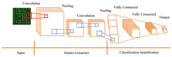
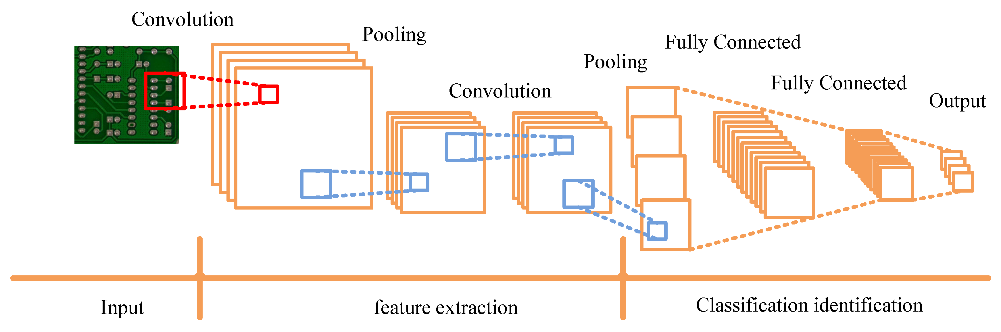
CNNs primarily process data with two-dimensional or three-dimensional structures such as images. Their architecture uses layers, including convolutional, pooling, dropout, and fully connected layers, to extract features and perform classification or regression tasks. Figure 1. illustrates this process, where an input image undergoes two convolutions, two pooling operations, and two fully connected layers within a typical CNN model, completing feature extraction followed by classification prediction.
Figure 1.
Schematic diagram of the convolutional neural network architecture.
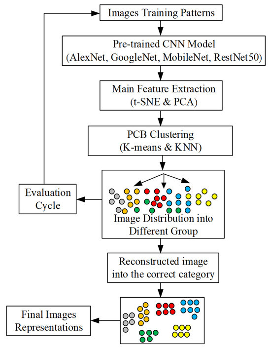
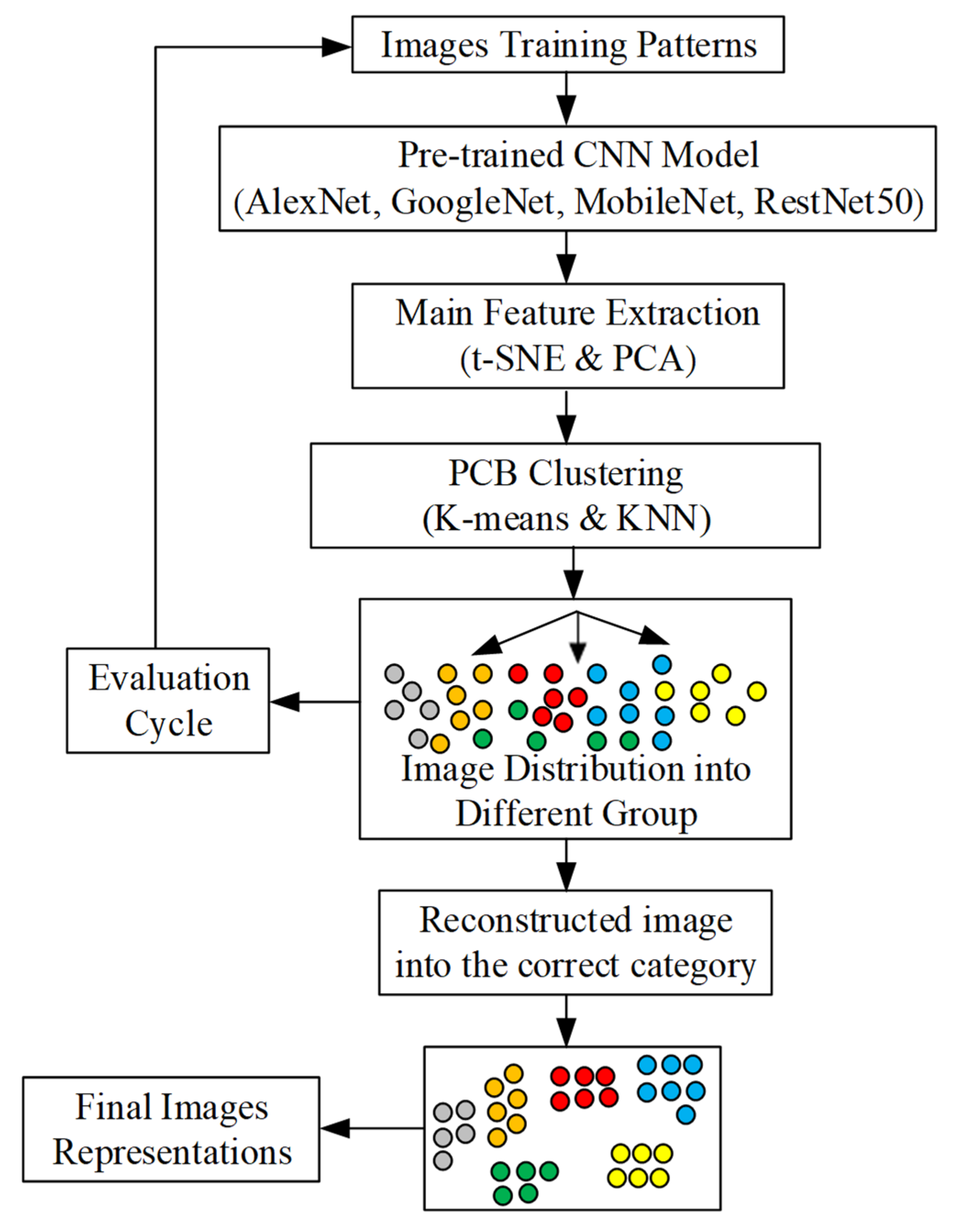
While CNNs achieve strong performance in image recognition [25], their training relies heavily on large datasets, creating challenges in data collection and computational demands. To address this, a hybrid CNN approach based on transfer learning was developed, which combines pretrained models, feature extraction, and dimensionality reduction classifiers, as illustrated in Figure 2.
Figure 2.
Hybrid convolutional neural network feature extraction and dimension reduction classifier.
The methodology implementation follows these steps:
- (1)
- Images training patterns:
Data collection: This stage involves gathering a substantial dataset of PCB defect images.
Annotation: Each image is meticulously annotated to label the location and type of defect present (e.g., missing hole, mouse bite, open circuit).
Dataset creation: The annotated images are organized into a structured training dataset, which is used to train the CNN model.
- (2)
- Pretrained CNN model:
Model selection: A pretrained CNN model suitable for PCB defect detection, such as AlexNet, GoogleNet, MobileNet, or ResNet50, is chosen.
Model fine-tuning: The pretrained model may undergo fine-tuning to adapt it specifically to the nuances of the PCB defect detection task, potentially leading to improved performance.
Feature extraction: The pretrained CNN model is employed to extract salient features from the input images, transforming each image into a representative feature vector.
- (3)
- Main feature extraction:
Dimensionality reduction: Techniques such as t-SNE or PCA are applied to reduce the dimensionality of the feature vectors, simplifying the data while retaining crucial information. This reduction in dimensionality helps mitigate computational complexity in subsequent steps.
Feature selection: Relevant features are selected from the reduced-dimensional vectors to increase the accuracy of classification.
- (4)
- PCB clustering:
Clustering algorithms: Clustering algorithms, such as K-means or KNN, are utilized to group the feature vectors. Each group ideally corresponds to a distinct type of PCB defect.
Cluster labelling: Each cluster is assigned a label that denotes the specific defect category it represents.
- (5)
- Evaluation cycle:
Performance evaluation: The effectiveness of the PCB defect detection system is assessed via a held-out test dataset. Metrics such as accuracy, recall, and the F1 score are employed to quantify performance.
Parameter tuning: On the basis of the evaluation results, the model parameters or algorithms may be adjusted to optimize detection performance.
- (6)
- Image distribution:
Classification: New, unseen PCB images are input into the trained model. The model classifies these images, assigning them to specific defect groups on the basis of their feature vectors.
- (7)
- Image reconstruction:
Defect localization: The model identifies and pinpoints the location and type of defect within the classified images.
Image reconstruction: The images with detected defects are reconstructed or highlighted to facilitate manual inspection and verification.
- (8)
- Final image representations:
Result output: The detection results are presented in a user-friendly format, either graphically (e.g., highlighting defect locations on the image) or textually (e.g., providing defect type and probability).
In this study, transfer learning was implemented via well-known pretrained models such as AlexNet, GoogleNet, MobileNet, and ResNet50 as the foundation.
AlexNet, proposed by Krizhevsky et al. in 2012 [26], comprises eight layers: five convolutional layers followed by three fully connected layers. It incorporates the rectified linear unit (ReLU) activation function, maximum pooling layers, local response normalization layers, and data augmentation to increase performance and stability.
GoogleNet, proposed by Szegedy et al. in 2014 [27], is a deep CNN architecture incorporating nine inception modules and auxiliary classifiers. Inspired by multiscale processing in biological vision systems, it employs parallel convolutional kernels of varying sizes and pooling layers to extract multilevel features. The architecture also uses 1 × 1 convolutional layers to reduce channel dimensionality and computational complexity. The input images undergo initial convolution before being processed by the inception modules. The feature vectors extracted from the output of the Loss3 classifier layer [28] are subsequently input to feature downscaling operations.
MobileNet, proposed by Howard et al. in 2017 [29], is a lightweight CNN architecture designed for mobile and embedded vision applications. It employs depthwise separable convolution to process input images. This technique decomposes standard convolution into depthwise convolution followed by pointwise (1 × 1) convolution. The feature vectors extracted from the final fully connected layer (logits) serve as inputs for subsequent dimensionality reduction operations, significantly reducing the computational cost and parameter count.
ResNet50, proposed by He et al. in 2015 [30], is a deep CNN architecture based on residual connections. It introduces residual learning, facilitating the training of deep networks and effectively addressing the degradation problem in which training error increases with network depth. ResNet50 employs residual blocks with bottleneck structures and cross-layer skip connections. This architecture enables the network to learn residual mappings, enhancing its representational capacity and generalization ability.
The classifiers within these models serve as preliminary feature extraction tools following their initial pretraining. The process involved removing the output layer from the selected model network, inputting PCB defect image samples into the modified pretrained network in a single forward pass, obtaining intermediate feature representations from the network, and then applying t-SNE or PCA algorithms for dimensionality reduction and feature extraction. These techniques identify essential features within the distribution values generated by the pretrained model and employ clustering algorithms to group features into their respective categories on the basis of their high similarity. This approach resulted in rapid PCB defect detection and an image classification system suitable for practical applications.
The methodology leveraging transfer learning for feature extraction in convolutional networks proceeded as follows: First, the original PCB defect sample image was selected and input into the chosen pretrained network model. The CNN then computes a feature vector representing the PCB defect image in a single computation. For example, an original image with dimensions of 1210 × 572 × 3 pixels was transformed into a feature vector of size 1000 × 2. Feature extraction was subsequently performed across various CNN models to analyse variations.
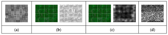
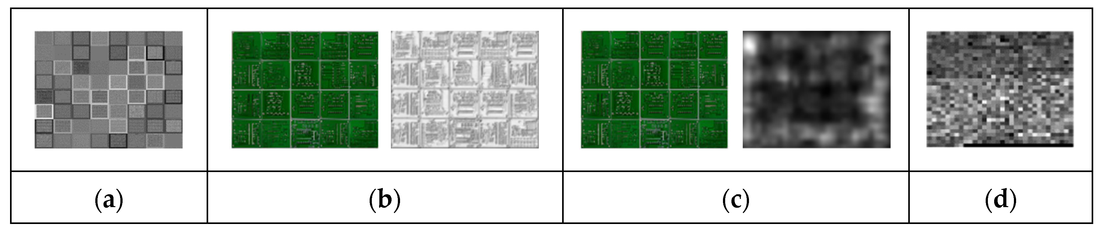
Figure 3. illustrates feature activations within the ResNet50 architecture:
Figure 3.
Examination of feature variations within the ResNet50 structural layers.
Figure 3a: Feature map from the Res2a_branch2c layer.
Figure 3b: Left: Original input image. Right: Activation map produced by a specific channel in Res2a_branch2c.
Figure 3c: Feature map from the Res5c_branch2c layer highlighting the strongest activation points.
Figure 3d: Feature distribution generated by the fc1000 layer output.
The feature maps extracted from the final convolutional layers across different CNN architectures, compared with the other models, ResNet50 yields superior structural representations of the input features. This characteristic contributes to its enhanced performance in PCB defect detection and recognition tasks.
3.2. Main Feature Extraction Process
Rawat and Wang [31] advanced deep CNN methodologies for feature extraction in image classification, addressing key implementation challenges. Niedzwiecki et al. [32] captured cosmic ray event imagery via the ESO database, implementing feature recognition and classification algorithms that categorized events into muon-like, electron-like, or other types. While t-SNE remains a widely adopted manifold learning algorithm for nonlinear dimensionality reduction, it inherently incurs feature information loss. Gao et al. [33] applied t-SNE within CNNs for hyperspectral image (HSI) applications to reduce postprocessing data dimensionality, demonstrating its efficacy for high-quality feature extraction across domains. Ma et al. [34] proposed a comprehensive and optimized method for image feature extraction based on object-based image analysis (OBIA) techniques in remote sensing from preprocessing to mapping. Notably, CNN feature extraction may propagate noise from original images that adversely impacts classification accuracy. To mitigate this limitation, our approach incorporates a dedicated dimensionality reduction layer [35] that employs t-SNE to process end-to-end CNN features.
To extract data features from the CNN system and input them into t-SNE calculations, we consider the following notation:
Let X = [x1, x2, …, xₙ] ∈ RCXN represent the vector of image data connected by the activation function in the pretrained CNN model. Here, N denotes the length of the image vector, C represents the vector size, and Y = [y1, y2, …, yₙ] is the output of the transformed vector X.
The conditional probability distributions P and Q are defined as follows:
where S(·) represents the Euclidean distance between two vectors of selected sample pixels. The Kullback–Leibler (KL) divergence in Equation (3) quantifies the difference between two distributions and should be minimized.
The t-SNE algorithm is a powerful method for dimensionality reduction and visualization. It projects high-dimensional data into a low-dimensional space while preserving the similarity between data points. Here is how it works:
- (1)
- Conditional probability calculation: First, we compute the conditional probability in the high-dimensional space, given an input data point x, and calculate the probability that it would pick another data point y as its neighbor if neighbors were chosen proportionally to their density under a Gaussian centered at x.
- (2)
- Low-dimensional space initialization: Next, we randomly initialize the joint probability in the low-dimensional space.
- (3)
- Minimizing the difference: Our goal is to minimize the difference between these probabilities and update the data positions in the low-dimensional space, and we measure this difference via an information-theoretic quantity called KL divergence, which reflects the dissimilarity between two probability distributions.
- (4)
- Gradient descent optimization: To achieve this minimization, we use gradient descent, an optimization technique that adjusts positions on the basis of partial derivatives of the difference with respect to each data point position, and we continue this process until reaching a local minimum or convergence.
- (5)
- Similarity calculation: The t-SNE algorithm computes the similarity between each pair of data points in the high-dimensional space and converts it into conditional probabilities.
- (6)
- Perplexity control: The similarity is defined on the basis of the Euclidean distance and variance of a Gaussian distribution, and perplexity, a parameter ranging from 5 to 50, controls the number of neighbors for each data point in the high-dimensional space.
PCA is a technique used to transform high-dimensional datasets into low-dimensional representations [36]. By combining data with similar patterns, PCA reduces the size of the training data. Specifically, PCA maps the original data features X = [x1, x2, …, xₙ] ∈ RCXN to a smaller output vector Y = [y1, y2, …, yₙ]. Here is how it works:
The eigenvalues and eigenvectors of the covariance matrix are calculated via singular value decomposition via the following equation:
where U and V are two orthogonal matrices. U represents all the eigenvectors of the calculated covariance matrix, and S is a diagonal matrix composed of eigenvalues. The low-dimensional feature Z is then obtained via the following formula.
Z is considered a smaller dataset, which extracts the main features reconstructed by the trained CNN model after transfer learning through the PCA algorithm.
3.3. Image Cataloging via K-Means or KNN Algorithms
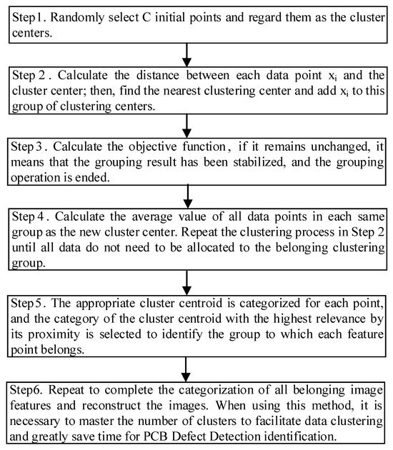
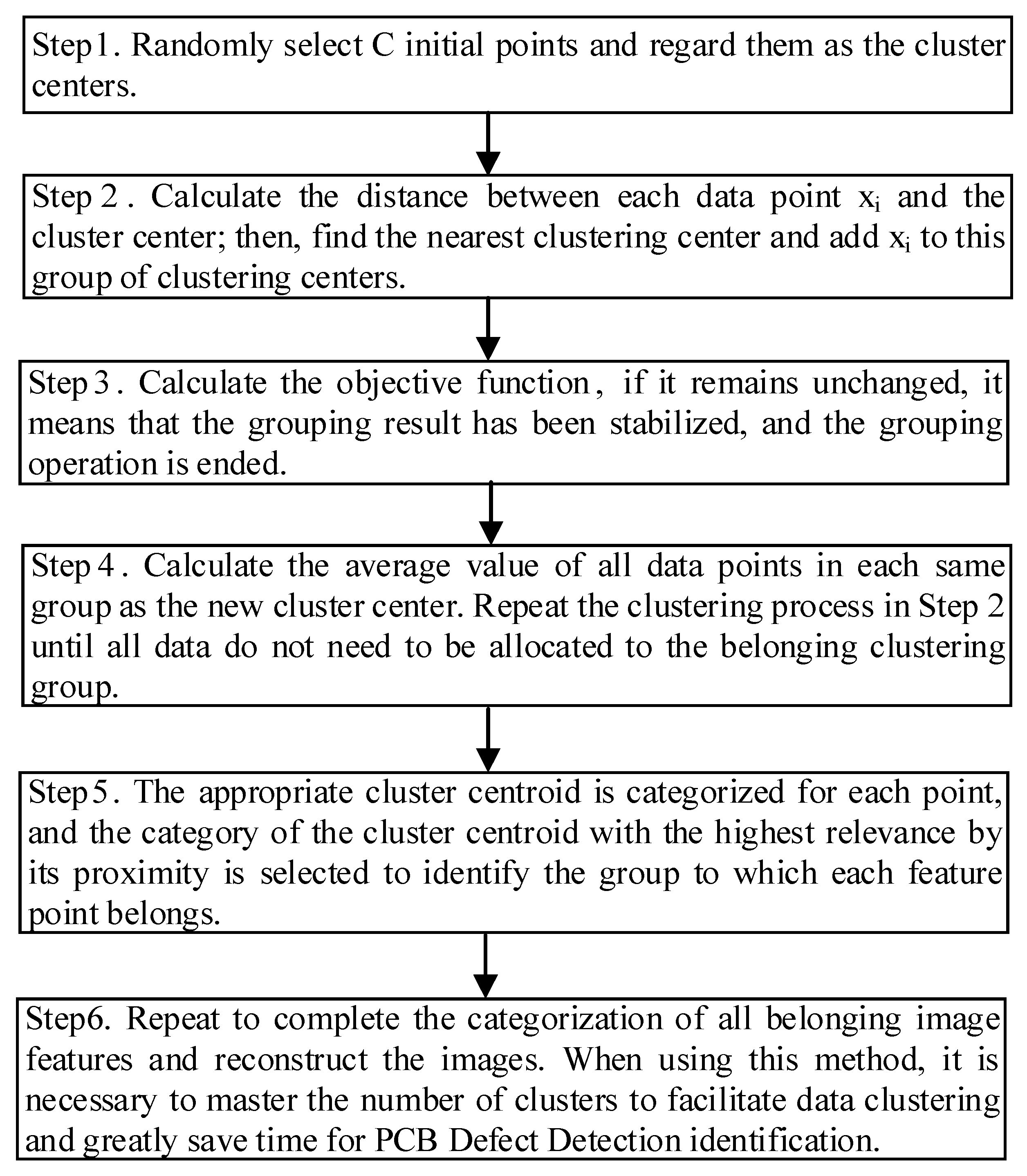
This study employs clustering algorithms to analyse the output distribution of main feature extraction process (MFEP) data for classifying PCB defect types. Our approach partitions the training dataset into K clusters to maximize intracluster similarity. The K-means algorithm, proposed by MacQueen in 1967, offers advantages of implementation simplicity, computational efficiency with large datasets, and scalability.
Given c clusters, we compute cluster centroids through K-means. The feature vectors assigned to the same cluster correspond to identical defect classes, driving subsequent PCB defect detection training, as illustrated in Figure 4.
Figure 4.
K-means training procedure for PCB defect detection.
The advantage of the K-means algorithm is that it does not require a large number of output nodes, which can greatly reduce the computational complexity. When this method is applied, the number of clusters must be known in advance, which facilitates data clustering and can greatly improve the timeliness of PCB defect detection type recognition.
Another algorithm is KNN, which is used to assign labels on the basis of the neighborhood of each data point [37]. First, we set a parameter k, which is the number of neighbors to consider when classifying. According to the definition of assignment, the category label that appears most frequently in the neighborhood will be assigned to the data point. The KNN classification algorithm is described in the following steps.
Step 1. Calculate the distance between all the data points and the considered data point;
Step 2. Select the k data points with the lowest distance values as the nearest neighbors;
Step 3. Retrieve the labels of all k neighbors;
Step 4. The label that appears most frequently among all the labels in step 3 is assigned to the considered data point.
4. Experiment Description and Result Analysis
Experimental simulations were performed on a Windows-based system equipped with an Intel Core i7-10610U CPU @ a 1.80 GHz processor and 16 GB of RAM. We conducted performance comparisons for PCB defect detection via four CNN architectures: AlexNet, GoogleNet, MobileNet, and ResNet50. Feature extraction was followed by analysis of technique combinations (t-SNE, PCA, K-means, KNN) and comprehensive performance evaluation.
The PCB defect dataset from Peking University Open Lab comprises 693 original images across six defect categories: missing holes, mouse bites, open circuits, short circuits, spurs, and spurious copper. Example images for each defect category are provided in Table 1, and the key characteristics of the dataset are summarized in Table 2.
Table 1.
PCB defect type and sample example.
Table 2.
Characteristics of the PCB defect dataset.
To address potential class imbalance and improve model generalizability, standard image augmentation techniques including random cropping, scaling, and splicing were applied to the training set. And all core hyperparameters were specified to ensure reproducibility. PCA retained components explaining 95% cumulative variance; t-SNE perplexity was set between 30 and 50 via grid search; K-means used K = 6 with 5 replicates; and KNN’s K was optimized via cross-validation, typically yielding K = 3 or 5.
4.1. Experiment
A consistent experimental pipeline was implemented across four pretrained CNN architectures for performance comparison. For each model, the process involved: (1) extracting high-dimensional feature vectors from the penultimate layer; (2) applying dimensionality reduction via either t-SNE or PCA; (3) clustering the reduced features using either the K-means or KNN algorithm for defect classification; and (4) reconstructing the classified images based on cluster indices for visualization. Each combination of techniques was evaluated over ten independent iterations.
As established in Section 3.1, ResNet50 provided the most distinct and structurally representative feature activations for PCB defects among the evaluated architectures. Consequently, a detailed analysis of its results is presented here. Following the standard pipeline, features extracted from ResNet50 were processed.
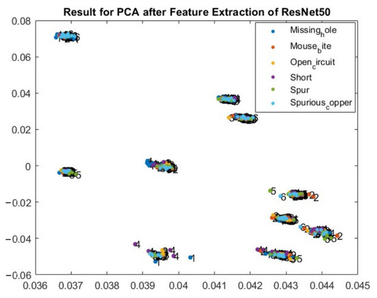
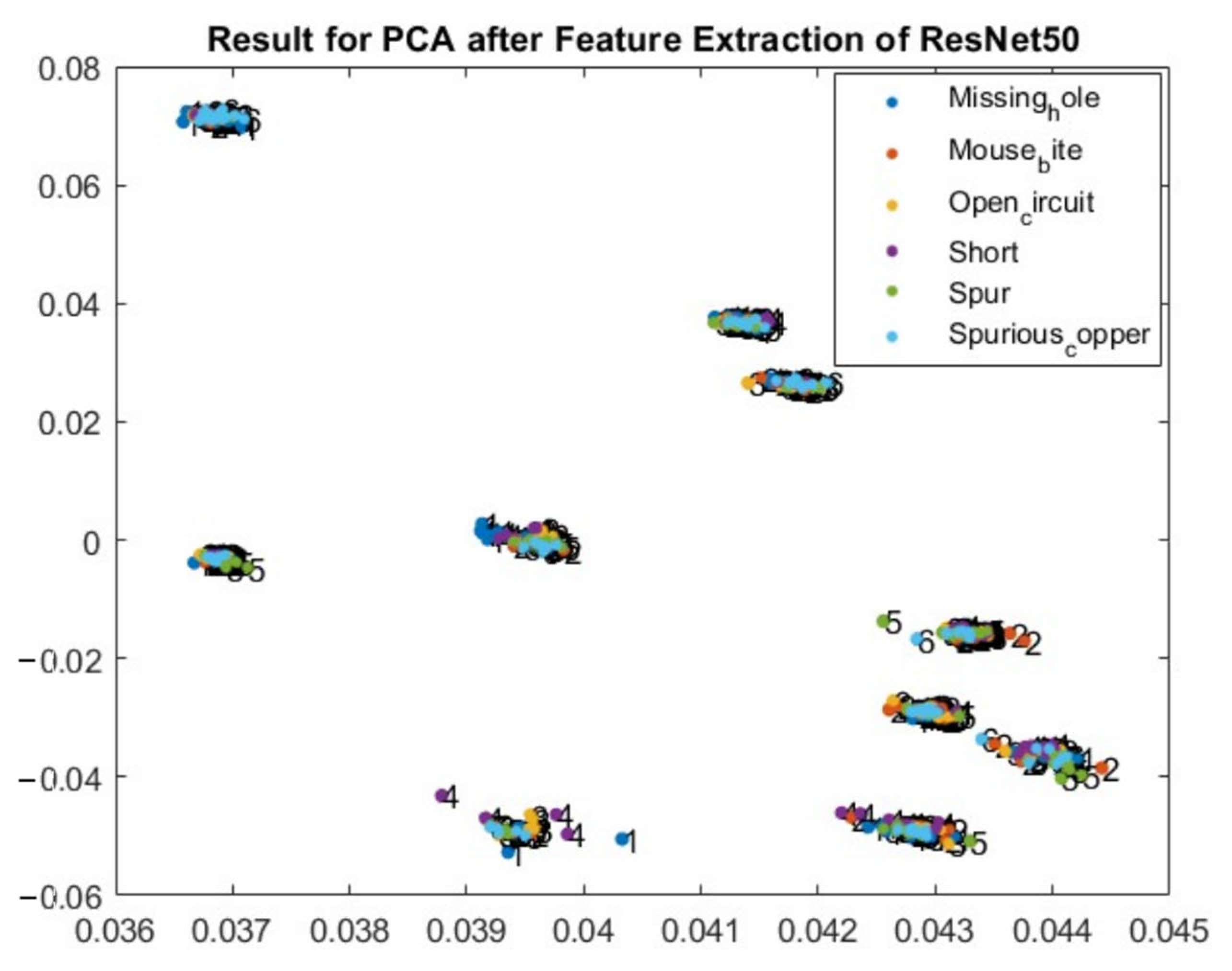
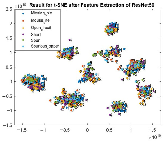
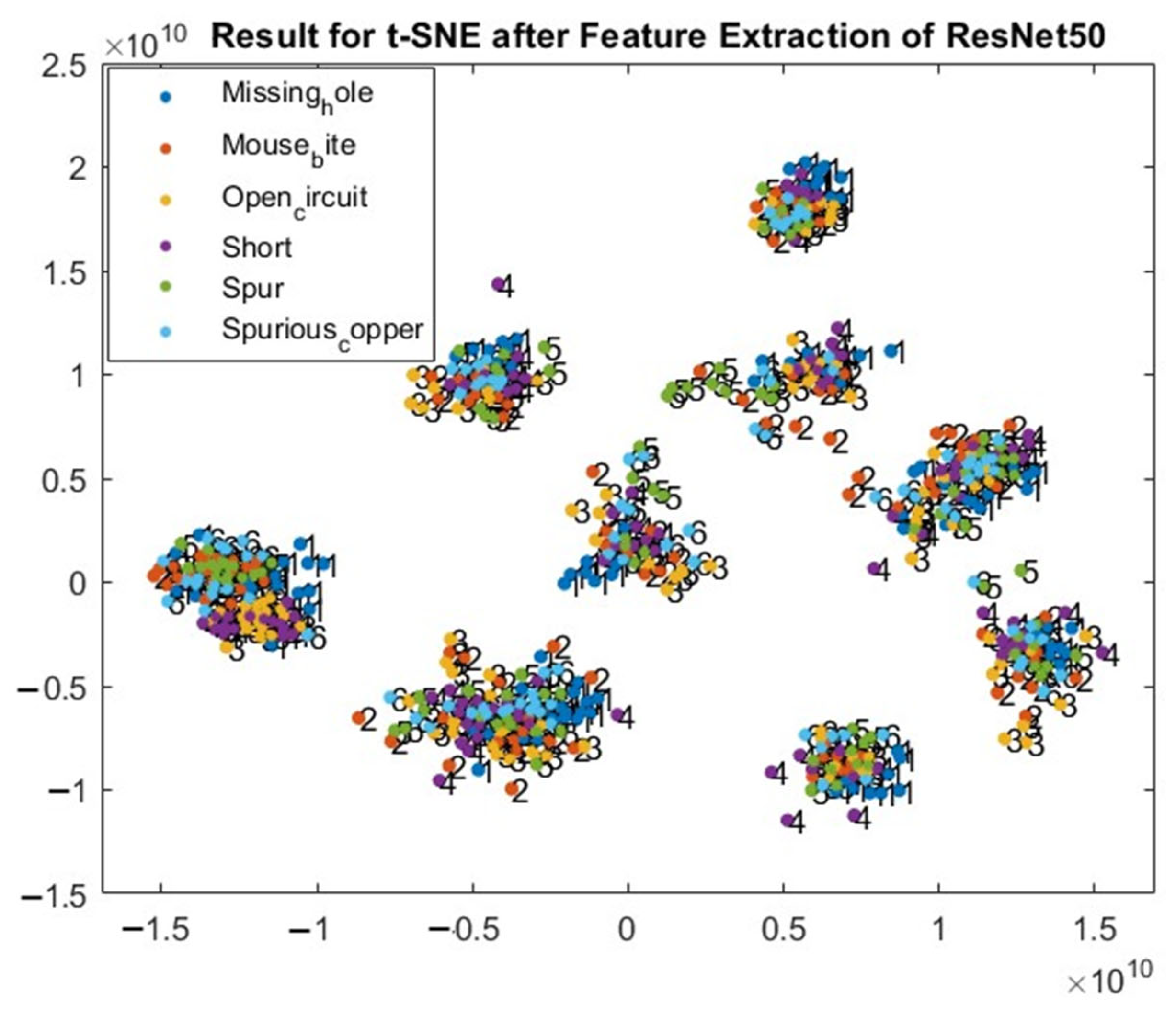
The distributions of the reduced-dimensional features are visualized in Figure 5 (PCA) and Figure 6 (t-SNE). The t-SNE projection, in particular, shows better separation between clusters corresponding to different defect types, suggesting its superior ability to preserve non-linear, discriminative structures in the ResNet50 feature space for this specific task. The subsequent image reconstructions based on the t-SNE + K-means clustering pathway are shown in Figure 7, effectively grouping and visualizing defects by category.
Figure 5.
Distribution of PCB defect types in ResNet50 after PCA feature extraction.
Figure 6.
Distribution of PCB defect types in ResNet50 after t-SNE feature extraction.
Figure 7.
Reconstruction of PCB defect types in ResNet50 via t-SNE and K-means.
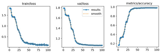
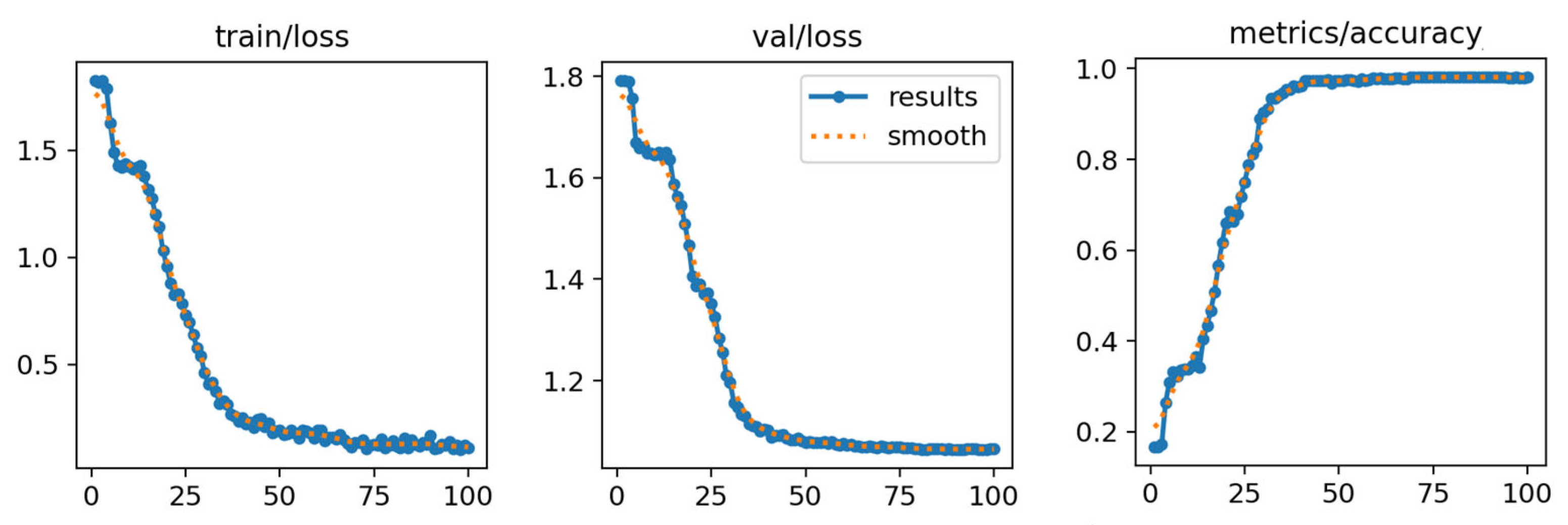
The training and validation loss curves are provided in Figure 8. The training loss exhibited a steady decline, confirming effective model optimization, and the highest accuracy reaches 97.33%.
Figure 8.
Training loss and validation loss.
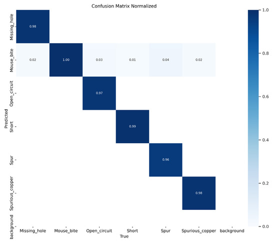
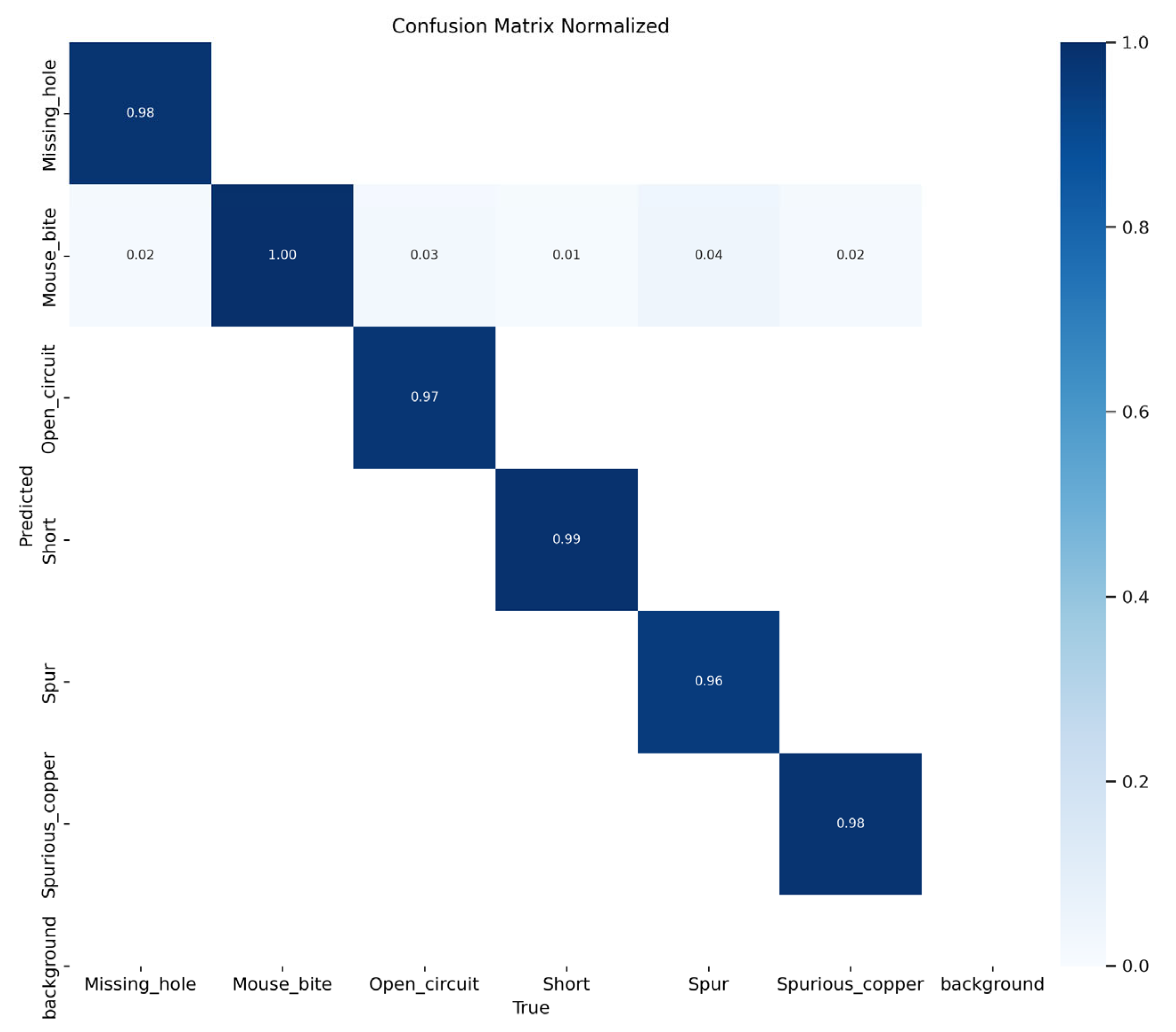
Figure 9 presents the normalized confusion matrix for the best-performing model on the test set. The matrix demonstrates strong overall classification performance, with high precision values concentrated along the main diagonal. Specific defect types, including Missing_hole, Mouse_bite, Spur, and Spurious_copper, are identified with near-perfect accuracy (>0.97). This detailed per-class analysis confirms the model’s high reliability for most defect types while highlighting a specific confusion that aligns with practical inspection challenges.
Figure 9.
Confusion matrix.
4.2. Performance Comparisons
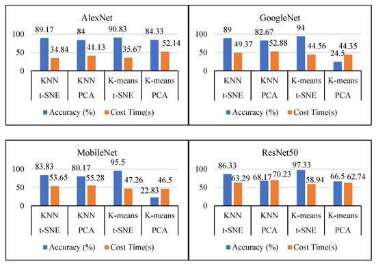
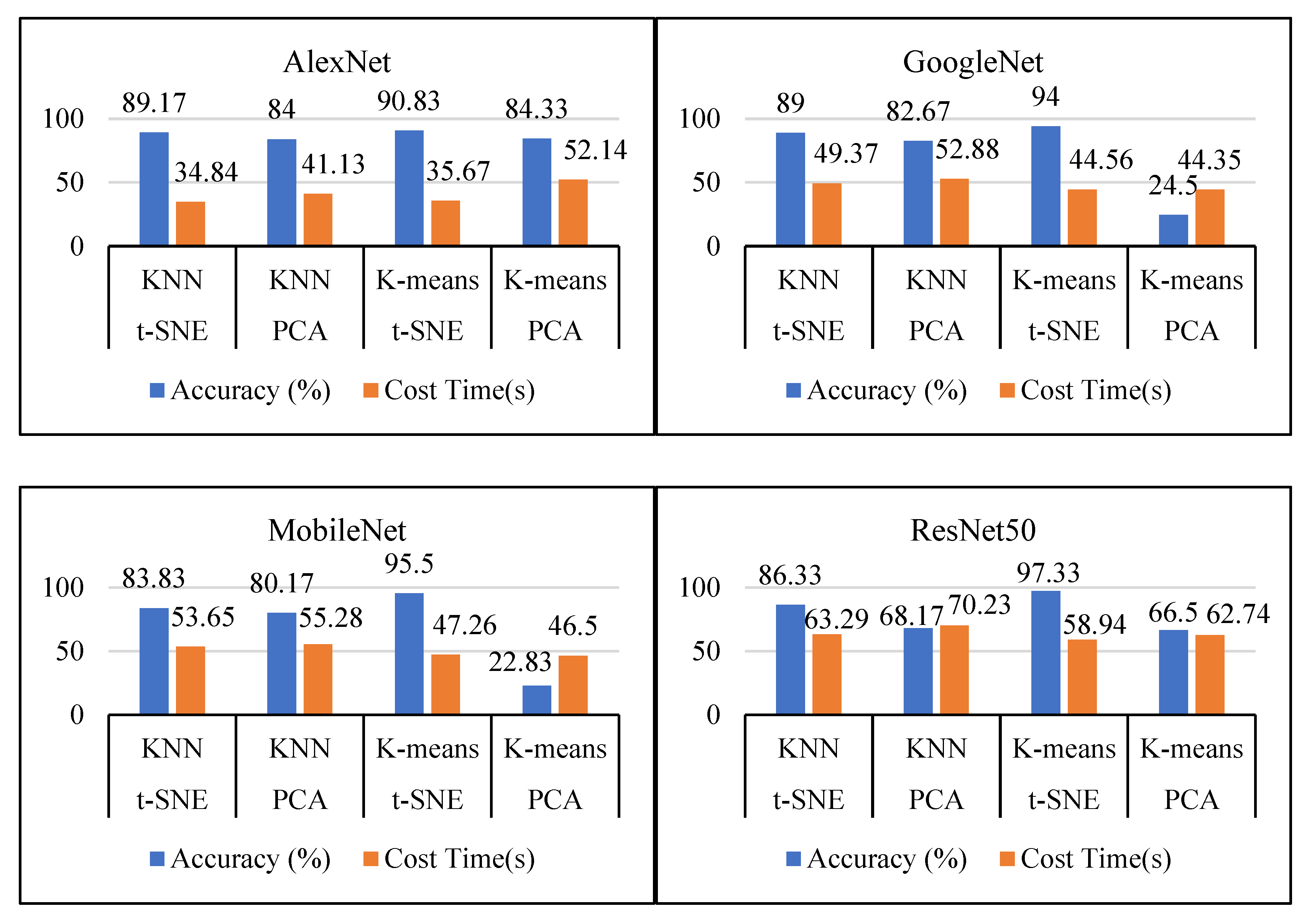
The comprehensive experimental results are presented in Figure 10. t-SNE leverages nonlinear conditional probability and Gaussian distributions to effectively separate data clusters across varying scales. For PCB defect recognition, CNN-based feature extraction reduces the original image dimensionality by approximately 1000×. Compared with PCA projections, t-SNE generates more distinct cluster separations, enabling faster convergence of the KNN and K-means algorithms during cluster formation.
Figure 10.
Performance analysis of various CNN model systems.
Among all 16 tested combinations, ResNet50 + t-SNE + K-means achieved the highest accuracy (97.33%). Other performant configurations include MobileNet + t-SNE + K-means (95.50%), GoogleNet+t-SNE+K-means (94.00%), and AlexNet + t-SNE + K-means (90.83%).
The experimental time cost analysis across the four CNN models (Table 3) reveals the following ascending order: AlexNet < GoogleNet < MobileNet < ResNet50. The AlexNet + t-SNE + KNN combination achieved the lowest computational time (34.84 s) but demonstrated relatively lower accuracy (90.83%). In contrast, the ResNet50 + t-SNE + K-means combination required 58.94 s (not the minimum time) while attaining the highest accuracy of 97.33%.
Table 3.
Performance analysis table of various CNN model systems.
5. Conclusions
This research has developed and systematically evaluated a hybrid framework for automated PCB defect detection, which strategically integrates transfer learning-based feature extraction, non-linear dimensionality reduction, and clustering-based classification. The core finding demonstrates that coupling a pretrained CNN, specifically ResNet50, with t-SNE and K-means clustering achieves a high-precision classification accuracy of 97.33% within a practical processing timeframe of approximately 60 s.
The principal advantage of our approach lies in its balanced resolution of three critical trade-offs in industrial inspection. By leveraging transfer learning, it achieves robust, data-efficient performance without requiring vast annotated PCB-specific datasets. It replaces the manual feature engineering of traditional methods with automated, adaptive feature learning from raw images, enhancing robustness to environmental and defect variations. Furthermore, by integrating intelligent dimensionality reduction and lightweight clustering after CNN feature extraction, the framework maintains high accuracy while significantly reducing computational complexity compared to heavier deep learning models, making it a practical and hardware-friendly solution for fast, inline quality control.
In summary, this work provides a validated, balanced solution that addresses the trilemma of data scarcity, the need for high accuracy, and computational constraints in industrial quality control. Future work will focus on further optimizing the pipeline’s latency and exploring its generalizability to other complex surface inspection tasks in manufacturing.
Author Contributions
Conceptualization, F.J.; Data curation, H.C.; Formal analysis, S.W.; Funding acquisition, F.J.; Investigation, H.C.; Methodology, F.J.; Project administration, S.W.; Resources, H.C.; Software, H.C.; Supervision, S.W. and C.C.; Validation, F.J. and H.C.; Visualization, F.J.; Writing—original draft, F.J.; Writing—review & editing, C.C.; All authors have read and agreed to the published version of the manuscript.
Funding
This research was supported by the High-Level Talent Research Start-up Funding Program of Xiamen Ocean Vocational College(KYG202202).
Data Availability Statement
Data are contained within the article. All data and related information used in this study are available from the corresponding authors upon reasonable request.
Conflicts of Interest
The authors declare no conflicts of interest.
References
- Quach, B.M.; Dinh, V.C.; Pham, N.; Huynh, D.; Nguyen, B.T. Leaf Recognition Using Convolutional Neural Networks Based Features. Multimed. Tools Appl. 2023, 82, 777–801. [Google Scholar] [CrossRef] [Scilit]
- Verdonck, T.; Baesens, B.; Óskarsdóttir, M.; Vanden Broucke, S. Special Issue on Feature Engineering Editorial. Mach. Learn. 2024, 113, 3917–3928. [Google Scholar] [CrossRef] [Scilit]
- Wu, F.; Zhang, X.; Kuan, Y.; He, Z. An AOI Algorithm for PCB Based on Feature Extraction. In Proceedings of the 2008 7th World Congress on Intelligent Control and Automation, Chongqing, China, 25–27 June 2008; IEEE: New York, NY, USA, 2008; pp. 240–247. [Google Scholar] [CrossRef] [Scilit]
- Soomro, I.A.; Ahmad, A.; Raza, R.H. Printed Circuit Board Identification Using Deep Convolutional Neural Networks to Facilitate Recycling. Resour. Conserv. Recycl. 2022, 177, 105963. [Google Scholar] [CrossRef] [Scilit]
- Wei, P.; Liu, C.; Liu, M.; Gao, Y.; Liu, H. CNN-based Reference Comparison Method for Classifying Bare PCB Defects. J. Eng. 2018, 2018, 1528–1533. [Google Scholar] [CrossRef] [Scilit]
- Ling, Q.; Isa, N.A.M. Printed Circuit Board Defect Detection Methods Based on Image Processing, Machine Learning and Deep Learning: A Survey. IEEE Access 2023, 11, 15921–15944. [Google Scholar] [CrossRef] [Scilit]
- Lim, J.; Lim, J.; Baskaran, V.M.; Wang, X. A Deep Context Learning Based PCB Defect Detection Model with Anomalous Trend Alarming System. Results Eng. 2023, 17, 100968. [Google Scholar] [CrossRef] [Scilit]
- Zheng, J.; Sun, X.; Zhou, H.; Tian, C.; Qiang, H. Printed Circuit Boards Defect Detection Method Based on Improved Fully Convolutional Networks. IEEE Access 2022, 10, 109908–109918. [Google Scholar] [CrossRef] [Scilit]
- Althubiti, S.A.; Alenezi, F.; Shitharth, S.; Sangeetha, K.; Reddy, C.V.S. Circuit Manufacturing Defect Detection Using VGG16 Convolutional Neural Networks. Wirel. Commun. Mob. Comput. 2022, 2022, 1070405. [Google Scholar] [CrossRef] [Scilit]
- Pratticò, D.; Carlo, D.D.; Silipo, G.; Laganà, F. Hybrid FEM-AI Approach for Thermographic Monitoring of Biomedical Electronic Devices. Computers 2025, 14, 344. [Google Scholar] [CrossRef] [Scilit]
- Meena, G.; Mohbey, K.K.; Indian, A.; Khan, M.Z.; Kumar, S. Identifying Emotions from Facial Expressions Using a Deep Convolutional Neural Network-Based Approach. Multimed. Tools Appl. 2023, 83, 15711–15732. [Google Scholar] [CrossRef] [Scilit]
- L, S.; V, S.; Ravi, V.; E.A, G.; K.P, S. Deep Learning-Based Approach for Multi-Stage Diagnosis of Alzheimer’s Disease. Multimed. Tools Appl. 2023, 83, 16799–16822. [Google Scholar] [CrossRef] [Scilit]
- Lu, Y.; Tao, X.; Jiang, F.; Du, J.; Li, G.; Liu, Y. Image Recognition of Rice Leaf Diseases Using Atrous Convolutional Neural Network and Improved Transfer Learning Algorithm. Multimed. Tools Appl. 2023, 83, 12799–12817. [Google Scholar] [CrossRef] [Scilit]
- Wu, X.; Ge, Y.; Zhang, Q.; Zhang, D. PCB Defect Detection Using Deep Learning Methods. In Proceedings of the 2021 IEEE 24th International Conference on Computer Supported Cooperative Work in Design (CSCWD), Dalian, China, 5–7 May 2021; IEEE: New York, NY, USA, 2021; pp. 873–876. [Google Scholar] [CrossRef] [Scilit]
- You, S. PCB Defect Detection Based on Generative Adversarial Network. In Proceedings of the 2022 2nd International Conference on Consumer Electronics and Computer Engineering (ICCECE), Guangzhou, China, 14–16 January 2022; IEEE: New York, NY, USA, 2022; pp. 557–560. [Google Scholar] [CrossRef] [Scilit]
- Kim, J.; Ko, J.; Choi, H.; Kim, H. Printed Circuit Board Defect Detection Using Deep Learning via A Skip-Connected Convolutional Autoencoder. Sensors 2021, 21, 4968. [Google Scholar] [CrossRef] [Scilit]
- Chen, I.-C.; Hwang, R.-C.; Huang, H.-C. PCB Defect Detection Based on Deep Learning Algorithm. Processes 2023, 11, 775. [Google Scholar] [CrossRef] [Scilit]
- Adibhatla, V.A.; Chih, H.-C.; Hsu, C.-C.; Cheng, J.; Abbod, M.F.; Shieh, J.-S. Applying Deep Learning to Defect Detection in Printed Circuit Boards via a Newest Model of You-Only-Look-Once. MBE 2021, 18, 4411–4428. [Google Scholar] [CrossRef] [Scilit]
- Sheraz, N.; Yasir, S. Enhanced Network Intrusion Detection Using Deep Convolutional Neural Networks. KSII TIIS 2018, 12, 5159–5178. [Google Scholar] [CrossRef] [Scilit]
- Tripathi, M. Analysis of Convolutional Neural Network Based Image Classification Techniques. J. Innov. Image Process. 2021, 3, 100–117. [Google Scholar] [CrossRef] [Scilit]
- Prasetyo, H.; Prayuda, A.W.H.; Hsia, C.H.; Wisnu, M.A. Integrating Companding and Deep Learning on Bandwidth-Limited Image Transmission. J. Internet Technol. 2022, 23, 467–473. [Google Scholar] [CrossRef] [Scilit]
- Hsia, C.-H.; Liu, C.-H. New Hierarchical Finger-Vein Feature Extraction Method for iVehicles. IEEE Sens. J. 2022, 22, 13612–13621. [Google Scholar] [CrossRef] [Scilit]
- He, P.; Ma, S.; Li, W. Efficient Barrage Video Recommendation Algorithm Based on Convolutional and Recursive Neural Network. J. Internet Technol. 2021, 22, 1241–1251. [Google Scholar] [CrossRef] [Scilit]
- Kordík, P.; Černý, J.; Frýda, T. Discovering Predictive Ensembles for Transfer Learning and Meta-Learning. Mach. Learn. 2018, 107, 177–207. [Google Scholar] [CrossRef] [Scilit]
- Shi, L.; Zhang, S.; Arshad, A.; Hu, Y.; He, Y.; Yan, Y. Thermo-Physical Properties Prediction of Carbon-Based Magnetic Nanofluids Based on an Artificial Neural Network. Renew. Sustain. Energy Rev. 2021, 149, 111341. [Google Scholar] [CrossRef] [Scilit]
- Krizhevsky, A.; Sutskever, I.; Hinton, G.E. ImageNet Classification with Deep Convolutional Neural Networks. Commun. ACM 2017, 60, 84–90. [Google Scholar] [CrossRef] [Scilit]
- Szegedy, C.; Liu, W.; Jia, Y.; Sermanet, P.; Reed, S.; Anguelov, D.; Erhan, D.; Vanhoucke, V.; Rabinovich, A. Going Deeper with Convolutions. In Proceedings of the 2015 IEEE Conference on Computer Vision and Pattern Recognition (CVPR), Boston, MA, USA, 7–12 June 2015; IEEE: New York, NY, USA, 2015; pp. 1–9. [Google Scholar] [CrossRef] [Scilit]
- Babu, H.; Venkatram, N. An Efficient Image Dahazing Using Googlenet Based Convolution Neural Networks. Multimed. Tools Appl. 2022, 81, 43897–43917. [Google Scholar] [CrossRef] [Scilit]
- Howard, A.G.; Zhu, M.; Chen, B.; Kalenichenko, D.; Wang, W.; Weyand, T.; Andreetto, M.; Adam, H. MobileNets: Efficient Convolutional Neural Networks for Mobile Vision Applications. arXiv 2017. [Google Scholar] [CrossRef] [Scilit]
- He, K.; Zhang, X.; Ren, S.; Sun, J. Deep Residual Learning for Image Recognition. In Proceedings of the 2016 IEEE Conference on Computer Vision and Pattern Recognition (CVPR), Las Vegas, NV, USA, 27–30 June 2016; IEEE: New York, NY, USA, 2016; pp. 770–778. [Google Scholar] [CrossRef] [Scilit]
- Rawat, W.; Wang, Z. Deep Convolutional Neural Networks for Image Classification: A Comprehensive Review. Neural Comput. 2017, 29, 2352–2449. [Google Scholar] [CrossRef] [Scilit]
- Niedzwiecki, M.; Rzecki, K.; Marek, M.; Homola, P.; Smelcerz, K.; Castillo, D.A.; Smolek, K.; Hnatyk, B.; Zamora-Saa, J.; Mozgova, A.; et al. Recognition and Classification of the Cosmic-Ray Events in Images Captured by CMOS/CCD Cameras. arXiv 2019, arXiv:1909.01929. [Google Scholar] [CrossRef] [Scilit]
- Gao, L.; Gu, D.; Zhuang, L.; Ren, J.; Yang, D.; Zhang, B. Combining T-Distributed Stochastic Neighbor Embedding with Convolutional Neural Networks for Hyperspectral Image Classification. IEEE Geosci. Remote Sens. Lett. 2020, 17, 1368–1372. [Google Scholar] [CrossRef] [Scilit]
- Ma, L.; Liu, Y.; Zhang, X.; Ye, Y.; Yin, G.; Johnson, B.A. Deep Learning in Remote Sensing Applications: A Meta-Analysis and Review. ISPRS J. Photogramm. Remote Sens. 2019, 152, 166–177. [Google Scholar] [CrossRef] [Scilit]
- Maaten, L.; Hinton, G.E. Visualizing Data Using T-SNE. J. Mach. Learn. Res. 2008, 9, 2579–2605. [Google Scholar]
- Yang, G.; Kothalil Gopalakrishnan, A. Network Traffic Threat Feature Recognition Based on a Convolutional Neural Network. In Proceedings of the 2019 11th International Conference on Knowledge and Smart Technology (KST), Phuket, Thailand, 23–26 January 2019; IEEE: New York, NY, USA, 2019; pp. 170–174. [Google Scholar] [CrossRef] [Scilit]
- Abdalla, H.I.; Amer, A.A. Towards Highly-Efficient k-Nearest Neighbor Algorithm for Big Data Classification. In Proceedings of the 2022 5th International Conference on Networking, Information Systems and Security: Envisage Intelligent Systems in 5g//6G-based Interconnected Digital Worlds (NISS), Bandung, Indonesia, 30–31 March 2022; IEEE: New York, NY, USA, 2022; pp. 1–5. [Google Scholar] [CrossRef] [Scilit]





Disclaimer/Publisher’s Note: The statements, opinions and data contained in all publications are solely those of the individual author(s) and contributor(s) and not of MDPI and/or the editor(s). MDPI and/or the editor(s) disclaim responsibility for any injury to people or property resulting from any ideas, methods, instructions or products referred to in the content. |
© 2026 by the authors. Licensee MDPI, Basel, Switzerland. This article is an open access article distributed under the terms and conditions of the Creative Commons Attribution (CC BY) license.