Article

Design and Simulation of Thermally Stable Lead-Free BaHfSe3 Perovskite Solar Cells: Role of Interface Barrier Height and Temperature

1
Department of Physics, Raja Narendra Lal Khan Women’s College (Autonomous), Midnapore 721102, West Bengal, India
2
Department of Physics, Ram Lakhan Singh Yadav College, Patliputra University, Bakhtiyarpur 803212, Bihar, India
3
Graduate School of Chemical Sciences and Engineering, Hokkaido University, Kita 13, Nishi 8, Kita-ku, Sapporo 060-8628, Japan
4
Research Center for Materials Nanoarchitectonics (MANA), National Institute for Materials Science (NIMS), 1-1 Namiki, Tsukuba 305-0044, Japan
5
Department of Physics, Trivenidevi Bhalotia College, Raniganj 713347, West Bengal, India
*
Authors to whom correspondence should be addressed.
Eng 2025, 6(12), 345; https://doi.org/10.3390/eng6120345 (registering DOI)
Submission received: 16 October 2025 / Revised: 10 November 2025 / Accepted: 12 November 2025 / Published: 1 December 2025

Abstract

Lead-free chalcogenide perovskites are emerging as promising alternatives to hybrid halide perovskites due to their superior thermal stability, non-toxicity, and strong optical absorption. In this study, the photovoltaic performance of single-junction BaHfSe3-based perovskite solar cells (PSCs) with the TCO/TiO2/BaHfSe3/Cu2O/Au configuration is systematically investigated using SCAPS-1D simulations. Device optimization identifies TiO2 and Cu2O as suitable ETL and HTL materials, respectively. The optimized structure—TCO/TiO2 (50 nm)/BaHfSe3 (500 nm)/Cu2O (100 nm)/Au—achieves a power conversion efficiency (PCE) of 24.47% under standard conditions. Simulation results reveal that device efficiency is influenced by absorber thickness and trap density. A detailed temperature-dependent study highlights that photovoltaic parameter efficiency is governed by the barrier alignment at the TCO/ETL interface. For lower TCO (Transparent Conducting Oxide) work functions (3.97–4.07 eV), PCE decreases monotonically with temperature, attributed to the increase in reverse saturation current resulting from a higher intrinsic carrier concentration. By contrast, higher TCO work functions (4.47–4.8 eV) yield an initial increase in efficiency with temperature, driven by reduced barrier height and favorable Fermi level shifts before efficiency declines at further elevated temperatures. These insights underscore the promise of BaHfSe3 as a lead-free, environmentally robust perovskite absorber for next-generation PSCs, and highlight the critical importance of interface engineering for achieving optimal thermal and operational performance.

1. Introduction

Perovskite solar cells (PSCs) have rapidly emerged as a leading next-generation photovoltaic technology owing to their remarkable power conversion efficiencies (PCEs), low-cost solution-processable fabrication routes, and highly tunable optoelectronic properties [1,2,3]. Organic–inorganic hybrid perovskites have especially dominated the field with certified PCEs exceeding 25%, [4] comparable to those of conventional silicon-based solar cells. More notably, perovskite/silicon tandem architectures have recently surpassed the Shockley–Queisser limit for single-junction silicon cells, achieving efficiencies above 33% [5]. Such advancements underscore the vast potential of PSCs for efficient solar energy conversion.
Despite impressive progress, the commercialization of PSCs remains constrained by their poor long-term operational stability. Conventional silicon photovoltaic modules are warranted for 20–25 years, setting a rigorous benchmark for alternative solar technologies. In contrast, PSCs suffer rapid degradation when exposed to environmental factors such as oxygen, moisture, ultraviolet (UV) radiation, temperature stress, and electric fields [6,7,8].
Significant efforts have been made to improve PSC stability through encapsulation, UV filtering, and defect passivation strategies [9]. However, thermal degradation remains a substantial and unavoidable challenge. During operation, solar modules often experience temperature rises of 40–45 °C above ambient, with effective operating ranges from −40 °C to +85 °C. According to IEC 61646 standards [10], sustaining long-term operational stability at 85 °C is mandatory for commercial qualification. Elevated temperatures induce complex degradation pathways, including chemical decomposition of perovskite components, structural phase transitions, morphological changes, and optical deterioration—all of which critically shorten device lifetimes.
Prior studies have demonstrated that thermal stress significantly affects hybrid PSC performance. For example, Conings et al. showed that MAPbI3-based devices degrade within 24 h at 85 °C even under inert atmospheres, primarily due to the evaporation of volatile halides and organic cations [11]. Habisreutinger et al. reported that organic hole-transport layers (HTLs) such as Spiro-OMeTAD, P3HT, and PTAA worsen thermal instability, whereas partial enhancements are attainable using inorganic transport layers or molecular passivation [12]. Enhanced thermal resilience is observed in cesium-based all-inorganic perovskites (CsPbX3; X = Cl, Br, I) and mixed-cation systems; Saliba et al. reported devices preserving 95% of their initial efficiency after 500 h at 85 °C [13]. More recently, p–i–n PSCs achieved record efficiencies near 24.6%, maintaining up to 96% and 88% of their performance after 1000 h of continuous operation at 25 °C and 75 °C, respectively, and surviving rapid thermal cycling between −60 °C and +80 °C [14]. Nonetheless, outdoor field tests reveal efficiency losses exceeding 15% within hours, highlighting ongoing challenges of thermal degradation [15].
These challenges have motivated exploration of thermally robust and environmentally benign alternatives to hybrid lead halide perovskites. Transition metal chalcogenide perovskites (TMCPs) with general formula ABX3 (where A = Ca, Sr, Ba; B = Ti, Zr, Hf; and X = S, Se) have emerged as promising candidates [16]. TMCPs are non-toxic, structurally stable, and possess semiconducting properties with tunable direct bandgaps ranging from 0.3 to 2.3 eV and high optical absorption coefficients exceeding 105 cm−1, comparable to traditional absorbers like GaAs. Importantly, the large band dispersion in Zr- and Hf-based TMCPs implies high carrier mobilities, essential for efficient charge transport. A comprehensive computational screening by Sun et al. identified materials such as CaTiS3, BaZrS3, CaZrSe3, and CaHfSe3 as potential solar absorbers with favorable optoelectronic properties [17].
Among these, BaZrS3 has been studied extensively due to its lead-free composition, exceptional environmental stability, and strong light absorption [18,19]. Its high absorption coefficient facilitates efficient carrier collection in thin-film configurations. The structurally analogous BaHfS3 is equally stable but exhibits a relatively wide bandgap (~1.9–2.0 eV), limiting its solar spectrum coverage. To overcome this, anion substitution strategies replacing sulfur with selenium yield BaZrSe3 and BaHfSe3, which have reduced bandgaps around 1.5 eV [18,20]. This red-shift originates from selenium’s larger ionic radius and lower electronegativity, enhancing orbital overlap and extending absorption into the visible–near-infrared range, rendering these selenide variants ideal for single-junction thermally stable photovoltaic applications. However, experimentally, only BaZrS3-based solar cells have been reported, achieving a modest PCE of 0.11% [21], whereas BaZrSe3 and BaHfSe3 remain unexplored experimentally, with existing studies limited to theoretical and simulation-based investigations.
Chalcogenide perovskites such as BaZrS3 and BaHfS3 are known for their excellent thermal and chemical stability, retaining their orthorhombic phase up to ~650 °C, far exceeding the stability of halide perovskites like CsPbBr3 (stable up to ~300 °C) [22]. Although BaHfSe3 has not yet been extensively studied, its close structural similarity to BaHfS3 and BaZrSe3 implies comparable robustness, with an estimated thermal stability up to ~500 K. To date, BaHfSe3 has not been experimentally synthesized, and no device reports exist. However, its predicted narrow bandgap (~1.5 eV) and structural similarity to stable Ba–Zr and Ba–Hf sulfides make it a promising candidate for lead-free and thermally robust photovoltaic applications.
Temperature-dependent studies have been conducted on Ba–Zr–based chalcogenide perovskites using SCAPS-1D simulations. For instance, Verma et al. observed a reduction in efficiency from 31.14% at 300 K to 29.98% at 500 K in FTO/CdS/BaZrSSe/Cu2O/Au devices [23]. Similarly, Kumar et al. simulated an Au/Cu2O/BaZrSSe3/WS2/FTO system and noted efficiency decline from 24% at 300 K to 20.6% at 400 K [24]. Mercy et al. reported a modest decrease from 32.58% to 31.79% when temperature increased from 300 K to 400 K in an FTO/ZrS2/Ba (Zr0.96Ti0.04)S3/SnS/Pt device [18]. These studies collectively suggest that the power conversion efficiency of Ba–Zr–based chalcogenide perovskites decreases monotonically with temperature.
However, the influence of interfacial energy alignment—particularly the barrier height at the transparent conducting oxide (TCO)/electron transport layer (ETL) interface—plays a decisive role in determining the temperature-dependent photovoltaic behavior. The barrier height directly affects charge extraction efficiency, interfacial recombination dynamics, and the variation of open-circuit voltage (Voc) with temperature [25,26]. Despite its potential importance, no comprehensive simulation study has yet quantitatively explored how barrier height modulation impacts the temperature dependence of photovoltaic parameters in chalcogenide perovskite solar cells.
In this work, we employ SCAPS-1D simulations to model and optimize the performance of a BaHfSe3-based single-junction perovskite solar cell (PSC) with the architecture TCO/ETL/BaHfSe3/HTL/Au. Alongside the selection and optimization of suitable ETL and HTL materials, we systematically investigate the combined effects of temperature and interfacial barrier height variations at the TCO/ETL interface. Furthermore, optimization of critical device parameters—including absorber thickness, trap density, and transport layer thickness—has been performed to establish a comprehensive understanding of the coupled thermal and interfacial influences on device performance. The insights derived from this study provide valuable guidance for designing thermally stable, lead-free chalcogenide perovskite solar cells with enhanced operational reliability.

2. Materials and Methods

SCAPS-1D has been widely used in the literature for solar cell simulation [27,28,29,30,31]. In this work, we employed SCAPS-1D (version 3.3.10), a one-dimensional solar cell simulation program developed by Prof. Marc Burgelman and colleagues at the University of Ghent, Belgium, to simulate and optimize the performance of BaHfSe3-based perovskite solar cells (PSCs) [32]. A planar n–i–p heterojunction architecture was adopted, comprising an electron transport layer (ETL), a BaHfSe3 absorber, and a hole transport layer (HTL), as illustrated in Figure 1. In this structure, the BaHfSe3 absorber serves as the intrinsic region between the p-type HTL and n-type ETL. Under illumination, photogenerated electron–hole pairs are separated by the built-in electric field at the heterojunction; electrons drift toward the ETL, while holes move toward the HTL, resulting in photocurrent generation.
Four ETLs (TiO2, SnS2, ZnSe, ZrS2) and four HTLs (MoO3, MoS2, Cu2O, and CZTS) were examined in the Transparent conducting oxide/ETL/BaHfSe3/HTL/Au configuration to identify the most efficient material combination. The effects of absorber thickness and defect densities (bulk and interfacial) were systematically optimized. All simulations were performed under AM 1.5 G illumination (100 mW/cm2, 1 sun) at 300 K. As transparent conducting oxide (TCO) Fluorine doped tin oxide (FTO) has been used. All input parameters for the device layers were obtained from previously reported studies and are summarized in Table 1, while the electrode parameters are provided in Table 2.
Table 1. Parameters for the different layers of proposed solar cell.
ETLBaHfSe3 [20]HTL
MaterialTiO2 [19]ZrS2 [18]ZnSe [33]SnS2 [34] Cu2O [19]MoO3 [34]CZTS [18]MoS2 [34]
Thickness (µm)0.040.040.040.040.50.10.10.10.1
Band gap (eV)3.22.52.811.851.52.1731.51.29
Electron affinity (eV)3.94.14.094.263.83.22.34.24.2
Dielectric permittivity (relative)916.48.617.7117.1118103
CB density of states (1/cm3)1.0 × 10212.2×10182.2×10187.32×10182.2×10182.02×10171.0×10192.2×10182.2×1018
VB density of states (1/cm3)2.0×10201.8×10191.8×10181.0×10191.8×10191.1×10192.2×10181.8×10191.9×1019
Electron mobility (cm/s)202.3×1034×102509.4×10 −22.0×1022101.0×102100
Hole mobility (cm/s)101.3×1031.1×101253.5×1028021025150
Donor density (1/cm3)2.0×10191.0×10151.0×10 189.85×10 1900000
Acceptor density (1/cm3)00001.0×10181.0×10 181.0×10 181.0×10 171.0×10 17
Table 2. Contact parameters in the simulation.
Contact/ParameterFront Contact (FTO)Back Contact (Au)
Metal work function, Φ m   (eV)4.07 [35]5.1 [36]
Electron thermal velocity1.0 × 1071.0 × 107
Hole Thermal Velocity1.0 × 1071.0 × 107
SCAPS-1D numerically solves the Poisson, carrier continuity, and drift–diffusion equations self-consistently to obtain current–voltage (J–V) characteristics, from which Voc, Jsc, FF, and power conversion efficiency (η) are determined. The governing equations are:
d 2 ψ d x 2 = E x = ρ ε = q ε [ p n + N D + N A ]
J n x = q G n R n ,
J p x = q ( G p R p )
J n = q n μ n E + q D n d n d x ,
  J p = q p μ p E q D p d p d x
Here, ψ   is the electrostatic potential, E   is the electric field, ρ is the charge density, p and n are hole and electron concentrations, μ n   and μ p   are mobilities, and D n and D p are the diffusion coefficients.
The Einstein relation, linking mobility and diffusion, is given by:
D ( n , p ) = k B T q μ ( n , p )
Hence, the diffusion coefficients vary proportionally with temperature, while carrier mobilities remain constant unless manually varied.
The temperature-dependent performance of the device was investigated over the range of 270–520 K. To examine the influence of the front contact on thermal behavior, simulations were performed using six different work function (WF) values (3.97, 3.98, 4.07, 4.47, 4.58 and 4.8 eV) for the TCO electrode. Varying the TCO work function effectively alters the interfacial energy alignment and the barrier height at the TCO/ETL interface, which critically governs carrier injection, extraction, and recombination processes. This approach enables a detailed understanding of how contact energetics modulate the temperature dependence of key photovoltaic parameters such as Voc, Jsc, FF, and overall device efficiency. In SCAPS-1D, only a few parameters such as conduction band density of states, valence band density of states, and thermal velocity of charge carriers vary intrinsically with temperature, expressed as:
N c = N c 0 ( T 300 ) 3 / 2 , N v = N v 0 ( T 300 ) 3 / 2 , v t h = v t h , 0 ( T 300 ) 1 / 2 .
These variations influence the intrinsic carrier concentration:
n i = N c N v e x p ( E g 2 k B T )
All other quantities—including band gap (E9), carrier mobilities, and defect parameters—remain fixed unless explicitly modified. The thermal velocities of electrons and holes were set to 107 cm/s at 300 K.
Although both band gap and mobility are generally temperature-dependent in semiconductors, no experimental or theoretical data are currently available for BaHfSe3. Given the chemical similarity to BaZrSe3, which exhibits a decreasing band gap with increasing temperature, [37] BaHfSe3 is expected to follow a similar trend. Therefore, while the temperature-dependent simulations maintained a fixed band gap, a separate analysis (see Supporting Information Figure S2) examined efficiency variation by changing the band gap from 1.5 eV to 1.4 eV and mobility.

3. Results and Discussion

3.1. Optimization of ETL and HTL Material

The conduction band minimum (CBM) of BaHfSe3 is positioned at 3.8 eV below the vacuum level, while its valence band maximum (VBM) lies near 5.3 eV. In designing efficient solar cells based on BaHfSe3 absorbers, the selection of appropriate electron transport layer(ETL) and hole transport layer (HTL) materials is crucial to enable effective charge extraction and minimize interfacial recombination losses. Specifically, for efficient electron transport, the ETL’s CBM should be aligned below (i.e., at a lower energy than) the BaHfSe3 CBM (value is greater than 3.8 eV since the energy is measured from vacuum, i.e., zero) to facilitate energetically favorable electron transfer toward the front contact or FTO electrode. Similarly, the HTL’s valence band edge should closely match or lie slightly above the BaHfSe3 VBM (around or less than 5.3 eV) to ensure efficient hole extraction toward the Au back electrode.
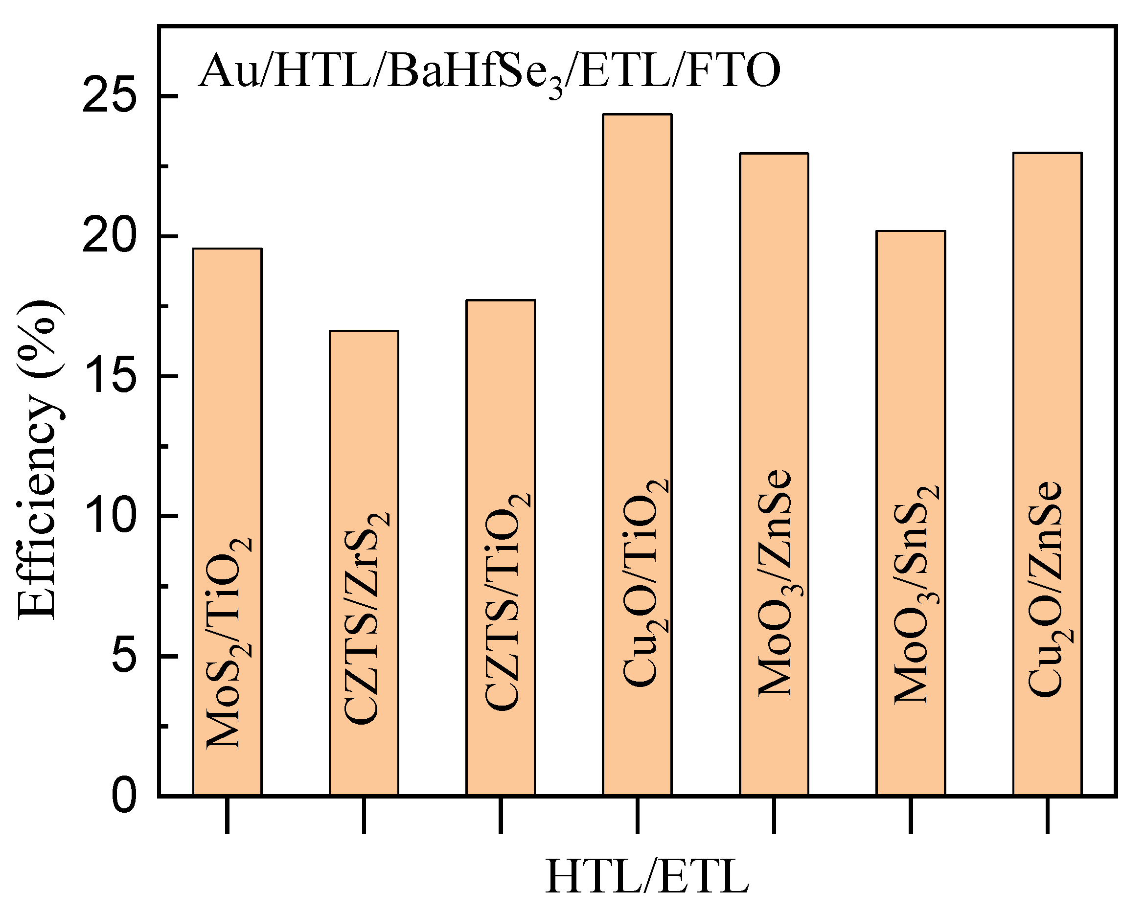
Guided by these criteria, several inorganic ETL and HTL materials were selected based on their reported band edge positions that closely satisfy these alignment conditions. The ETL candidates include TiO2, ZrS2, ZnSe, and SnS2, all possessing conduction band minima ideally placed relative to BaHfSe3. For the HTL, materials such as MoS2, Cu2O, Cu2ZnSnS4 (CZTS), and MoO3 were chosen for their suitable valence band maxima favorable for hole transport (Figure 1b). Different combinations of ETL and HTL materials were used in the device configuration FTO/ETL (50 nm)/BaHfSe3 (400 nm)/HTL (100 nm)/Au, and their photovoltaic performances were systematically simulated using SCAPS-1D to get the best efficiency.
The simulation results, summarized in Figure 2, reveal that the device incorporating TiO2 as the ETL and Cu2O as the HTL demonstrates the highest power conversion efficiency, reaching 24.15%. This superior performance is attributed to the optimal band alignment provided by TiO2 and Cu2O with respect to BaHfSe3, enabling efficient charge separation and extraction while minimizing recombination at the interfaces. Other ETL/HTL combinations exhibited lower efficiencies, reflecting less favorable band alignment or increased interfacial losses. These findings highlight the critical importance of carefully matching ETL and HTL band edges with the absorber’s electronic structure to maximize device efficiency in BaHfSe3-based perovskite solar cells.

3.2. Optimization of Absorber Layer Thickness

After selecting the optimal device structure, the thickness of the BaHfSe3 absorber layer was systematically optimized, as it critically influences the photovoltaic performance of PSCs. An appropriate absorber thickness must balance efficient light absorption and effective charge carrier collection. An absorber that is too thin results in incomplete photon absorption, reducing the short-circuit current density ( J s c ) and overall efficiency. Conversely, excessively thick layers contribute to increased bulk recombination, which degrades device performance.
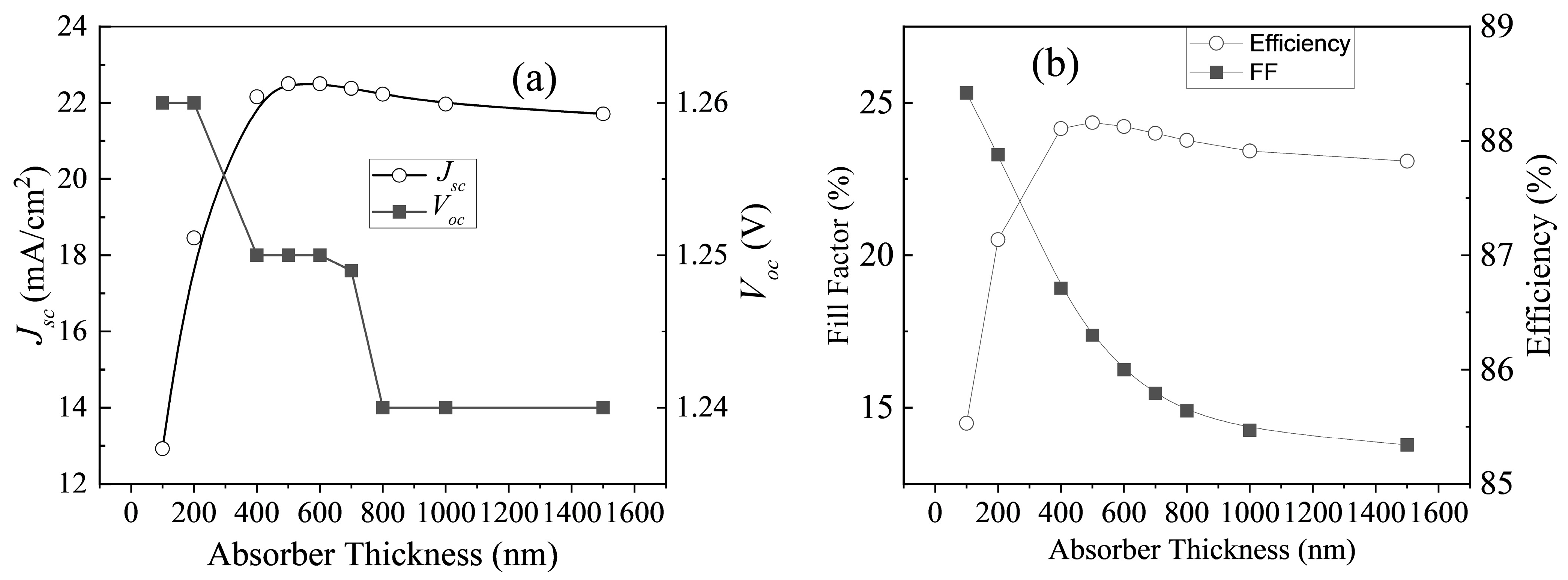
Our simulations reveal that J s c increases steadily with the absorber thickness, reaching a saturation point near 500 nm where the efficiency peaks at 24.47% (Figure 3a). The efficiency remains relatively stable between 500 nm and 700 nm, indicating an optimal thickness range where the benefit of increased photon absorption offsets recombination losses. Beyond 700 nm, efficiency declines progressively, reaching 23.09% at 1500 nm thickness (Figure 3b). This degradation is attributed to elevated recombination rates within the thicker absorber, which increase the dark saturation current and subsequently reduce the V o c as demonstrated in Figure 3a.
The gradual decrease in fill factor (FF) observed with increasing thickness further supports the presence of enhanced carrier recombination and series resistance. The combined effect of saturation in J s c , rising recombination, and increasing saturation current explains the observed efficiency trend. Our results indicate that the absorber thickness range of 500–700 nm provides the best trade-off between photon absorption and charge extraction, maximizing power conversion efficiency before performance deteriorates at higher thicknesses.

3.3. Optimization of ETL and HTL Layers Thickness

Optimization of the ETL and HTL layers was also carried out by varying their thicknesses from 10 nm to 500 nm. The corresponding results are provided in the Supporting Information (Figure S1). The variation in photovoltaic parameters with layer thickness was found to be negligible, indicating that both ETL and HTL layers primarily serve charge transport and selective contact roles rather than contributing significantly to optical absorption. Therefore, an ETL thickness of 50 nm and an HTL thickness of 100 nm were selected for the optimized device structure.
The HTL thickness was chosen slightly higher to ensure complete coverage of the absorber surface, thereby minimizing interfacial recombination and improving hole extraction uniformity. A thicker HTL also helps in reducing shunt pathways and enhancing the overall stability of the device without significantly affecting series resistance. This thickness-dependent behavior aligns well with previous theoretical and experimental observations in perovskite solar cells, underscoring the importance of tailoring absorber dimensions for optimized device operation [38,39].
The optimized BaHfSe3-based perovskite solar cell, structured as TCO/TiO2 (50 nm)/BaHfSe3 (500 nm)/Cu2O (100 nm)/Au, achieves a short-circuit current density (Jsc) of 22.61 mA/cm2, an open-circuit voltage (Voc) of 1.25 V, a fill factor (FF) of 86.29%, and a power conversion efficiency (PCE) of 24.47% under standard testing conditions (trap density of 1014 cm−3, room temperature 300 K). This performance highlights the exceptional promise of lead-free chalcogenide perovskites for highly efficient and stable solar cell applications, with device metrics closely comparable to the leading results in the contemporary perovskite research field.

3.4. Evaluation of the Shockley–Queisser Efficiency Limit and the Role of Radiative Recombination

To benchmark the simulated performance of the BaHfSe3-based perovskite solar cell, the theoretical Shockley–Queisser (SQ) efficiency limit was estimated based on its optical bandgap (E9 = 1.50 eV). Under standard AM1.5G illumination (ASTM G-173 [40]), the corresponding SQ limit is approximately 31–32%, which represents the maximum attainable efficiency when radiative recombination is the only loss mechanism.
In practical photovoltaic devices, however, radiative recombination contributes significantly to carrier losses and reduces the overall efficiency. Since BaHfSe3 is a relatively new and less-explored lead-free perovskite, there are currently no reported theoretical or experimental values for its radiative recombination coefficient (B). To address this uncertainty and to assess its potential influence on device performance, a systematic simulation study was performed by varying B over a wide range from 10−9 to 10−13 cm3 s−1 using the SCAPS-1D framework.
The results of this parametric study are summarized in Supplementary Material (Figure S2). A clear trend was observed where the power conversion efficiency (PCE) decreases with increasing radiative recombination rate. Specifically, the efficiency drops from 24.77% for B = 0 cm3 s−1 (no radiative recombination) to about 19% for B = 1013 cm3 s−1, and further down to approximately 5% for B = 109 cm3 s−1. This pronounced reduction demonstrates the detrimental impact of radiative losses and provides a realistic projection of device efficiency under practical conditions, where radiative recombination cannot be fully suppressed.
All final simulations presented in this manuscript were carried out using B = 0 cm3 s−1 to represent the upper theoretical limit of performance for the optimized device structure. Importantly, even under this idealized condition, the obtained efficiency (≈24.77%) remains well below the SQ limit of 31–32%, confirming that the chosen material and device parameters are physically reasonable and do not involve any overestimation. The variation of efficiency with B further illustrates the performance degradation expected under realistic recombination scenarios, offering valuable insight into the potential efficiency range achievable in experimental BaHfSe3-based solar cells.

3.5. Effect of Absorber Thickness and Trap Density on Device Performance

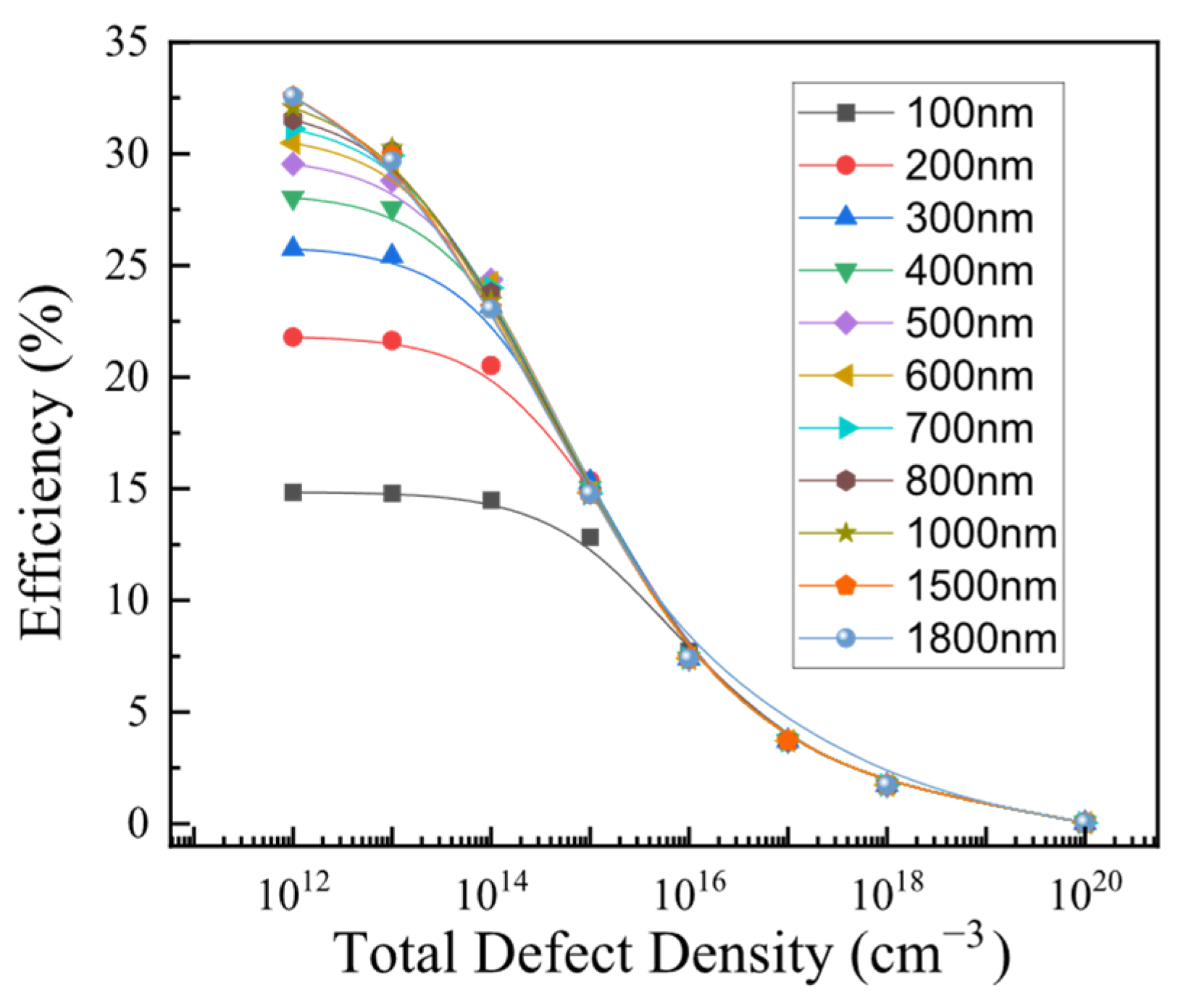
Our SCAPS-1D simulations systematically elucidate the critical interplay between absorber thickness d and bulk trap density N t in determining perovskite solar cell efficiency. Key trends emerge from defect-related recombination physics and optical absorption considerations. The findings are shown in Figure 4.
Low trap density regime ( N t 10 13   cm 3 ): The minority carrier diffusion length L is much greater than d ( L d ), enabling nearly all photogenerated carriers to be collected efficiently. Increasing d improves light absorption and thus short-circuit current density J s c , resulting in monotonically increasing power conversion efficiency (PCE). Efficiency tends to saturate at very high thicknesses ( > 1500 nm) as absorption approaches completeness and marginal gains diminish.
Moderate trap density regime ( N t 10 14   cm 3 ): The diffusion length becomes comparable to d ( L d ), yielding an optimal absorber thickness around 500–700 nm. Thinner devices suffer from insufficient photon absorption causing low J s c , while thicker films experience pronounced Shockley-Read-Hall (SRH) recombination losses, which reduce carrier collection efficiency and degrade performance beyond 800 nm.
High trap density regime ( N t 10 17   cm 3 ): SRH recombination dominates; carrier lifetimes and diffusion lengths shrink drastically ( L d ), causing rapid recombination before carriers reach contacts. Here, J s c and overall efficiency become largely independent of thickness and converge to a low value (~3.7%), reflecting severe recombination losses regardless of d .
These behaviors can be quantitatively described by the SRH carrier lifetime τ and diffusion length L , which link defect density directly to transport and collection efficiency:
τ = 1 σ v t h N t
L = D τ
where σ = capture cross-section of traps, v t h = carrier thermal velocity, D = diffusion coefficient.
Higher N t reduces τ , shortening L and impairing collection efficiency, affecting J s c , V o c , and FF.

3.6. Role of Transparent Conducting Oxide (Front Contact) Work Function

The work function (ΦTCO) of transparent conducting oxides (TCOs) plays a pivotal role in governing the performance of optoelectronic devices, including organic and perovskite solar cells (PSCs). It critically determines the energy band alignment at the TCO/electron transport layer (ETL) interface, thereby influencing charge extraction efficiency, carrier recombination dynamics, and ultimately the open-circuit voltage. Several studies have demonstrated that surface modification of TCOs can substantially enhance device performance. For instance, Lee et al. reported a 3.6% improvement in power conversion efficiency (PCE) by introducing a MoO3-graded ITO anode [41] while Lei et al. achieved an improvement PCE of 7.4% by incorporating a CuS interlayer on ITO [42].
A systematic simulation-based investigation of device behavior as a function of TCO work function is therefore essential—not only for optimizing photovoltaic performance but also for interpreting temperature-dependent trends in PSCs. Such computational insights can guide targeted experimental strategies for TCO surface engineering, enabling enhanced interfacial alignment and superior thermal stability in next-generation perovskite. Indium tin oxide (ITO), a commonly used TCO, has a tunable WF that can be controlled via oxidative treatments such as oxygen plasma, UV-ozone exposure, or chemical oxidation. These treatments alter surface dipoles and electronic states, allowing Φ ITO to vary typically between 3.95 eV and 5.11 eV, as reported earlier [43].
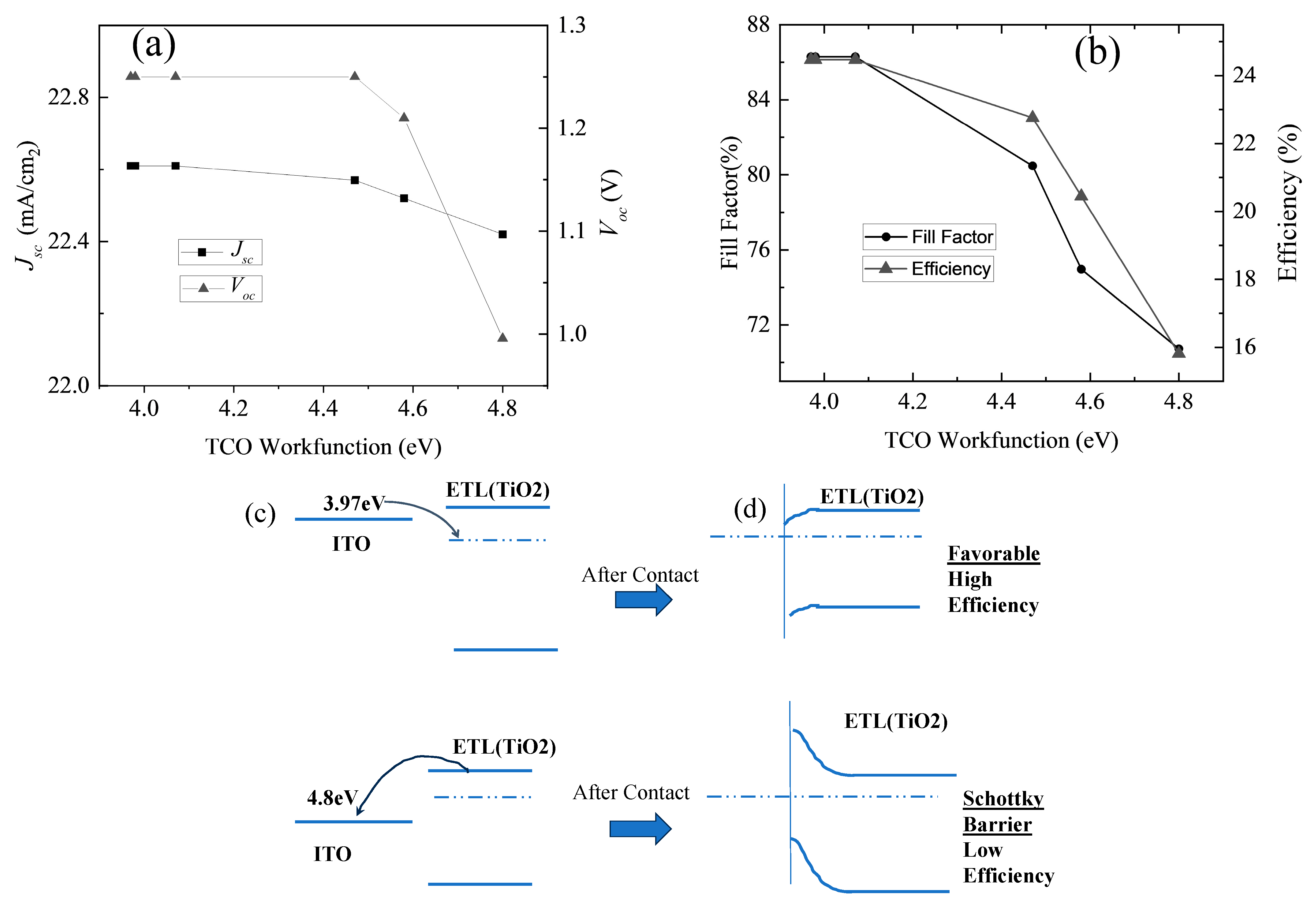
In this work, we systematically varied the ITO WF from 3.97 to 4.8 eV and examined its influence on key photovoltaic parameters: short-circuit current density ( J sc ), open-circuit voltage ( V oc ), fill factor (FF), and power conversion efficiency ( η ). As illustrated in Figure 5a,b, all these parameters decrease as the value of TCO WF increases (i.e., shifts deeper below the vacuum level). Specifically, V oc remains nearly constant at approximately 1.25 V for Φ TCO = 3.97 4.07   eV , but declines beyond this range, reaching approximately 0.99 V at Φ TCO = 4.8   eV . Correspondingly, FF and η follow a similar downward trend, implying increased series resistance and reduced charge extraction efficiency. J sc also decreases with increasing Φ TCO , likely due to enhanced interfacial barriers causing minor transport limitations.
This behavior is explained by the variation in the interfacial barrier height ( Φ B ) formed between ITO and the ETL (typically TiO2). The barrier height is defined as:
Φ B = Φ TCO χ ETL
where Φ TCO is the TCO WF and χ ETL is the electron affinity (conduction band minimum, CBM) of the ETL.
Figure 5c illustrates the energy level alignment of the ITO work function (WF), conduction band minimum (CBM), valence band maximum (VBM), and the Fermi level of the ETL layer before contact. When the ITO work function is relatively low (e.g., 3.97 eV), it lies above the Fermi level of the n-type TiO2 layer. Upon contact, electrons transfer from the ITO electrode to the TiO2 layer until Fermi level equilibrium is achieved. This electron flow leads to the accumulation of negative charge on the TiO2 side, resulting in a downward band bending at the TCO/ETL interface, as shown in Figure 5d.
Conversely, when the ITO work function is higher (e.g., 4.8 eV) and lies deeper than the Fermi level of TiO2, electrons move from the TiO2 layer to the ITO during equilibration. This process leaves behind positively charged donor ions near the TiO2 interface, leading to an upward band bending. These two distinct interfacial alignments crucially affect the barrier height, carrier transport, and open-circuit voltage (Voc) behavior, which are further discussed in the following section.
Case 1: ITO Work Function Φ ITO = 3.97 4.07   eV (Lower Work Function)
In this case, the ITO Fermi level lies above the TiO2 CBM at 3.9 eV (shallower energy level), resulting in a minimal or negligible barrier height: Φ B = 3.97 3.9 = 0.07   eV no   effective   barrier .
Electrons in TiO2 can move “downhill” energetically toward the ITO electrode with very little resistance. This favorable alignment results in downwards band bending on the TiO2 side at the interface, promoting efficient electron extraction and low recombination losses as shown in Figure 5a. Consequently, devices show stable and higher J sc , F F , V o c   a n d   η in that range.
Case 2: ITO Work Function Φ ITO = 4.7 4.8   eV (Higher Work Function)
In this case, the Fermi level of ITO lies below the conduction band minimum (CBM) of TiO2, forming a Schottky barrier at the TCO/ETL interface. The barrier height can be estimated as Φ B = 4.8 4.2 = 0.6   eV . This results in upward band bending on the TiO2 side near the interface, as illustrated in Figure 5b. Such an interfacial energy barrier hinders electron transfer from TiO2 to ITO, thereby enhancing interface recombination and increasing series resistance. Consequently, electron extraction efficiency is reduced. As the ITO work function increases, the corresponding barrier height also increases, leading to a monotonic decline in Voc, FF, and overall power conversion efficiency (η).

3.7. Temperature Dependence of Photovoltaic Parameters

The temperature dependence of photovoltaic parameters strongly influences the operational performance of solar cells. With increasing temperature, band gap narrowing, carrier mobility degradation, and interface barrier modification collectively affect the open-circuit voltage (Voc), short-circuit current density (Jsc), fill factor (FF), and power conversion efficiency (PCE). Among these factors, the work function (WF) of the transparent conducting oxide (TCO) layer is particularly critical, as it determines the built-in potential and barrier height at the front interface. Moreover, tuning the TCO work function is experimentally more feasible than modifying intrinsic semiconductor parameters, making it a practical route for optimizing temperature-dependent performance.
Since 1D SCAPS simulations do not account for temperature-induced changes in band gap and carrier mobility, these parameters were independently varied to understand their qualitative effects on efficiency. For BaHfSe3, the band gap was varied from 1.5 eV to 1.4 eV, corresponding to a temperature range of 270–500 K. The PCE increased from 24.47% to 25.77%, indicating that band gap narrowing exerts a positive influence as it approaches the optimal single-junction band gap. The variation of the parameters is shown in Supplementary Materials (Figure S3). Conversely, assuming carrier mobility follows μ ∝ T−0·5, efficiency decreased from 24.47% at 300 K to 17.73% at 500 K, showing a negative temperature effect. The detailed results are provided in the Supporting Information (Figure S4). Overall, band gap narrowing slightly enhances efficiency, while mobility degradation dominates, leading to a net decrease in performance with temperature.
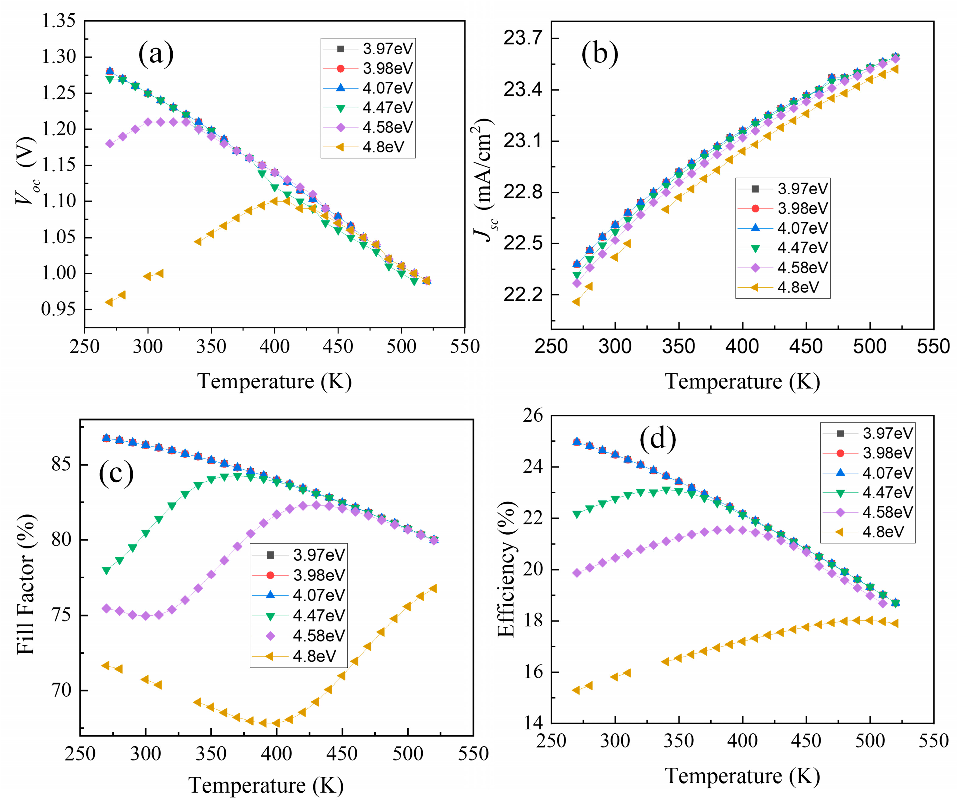
After confirming these trends, we systematically examined the impact of TCO work function variation on temperature-dependent device characteristics. The WF of TCO was varied from 3.97 eV to 4.80 eV, and the corresponding Voc, Jsc, FF, and PCE values were analyzed with temperature. As shown in Figure 6, Voc and PCE exhibit similar temperature-dependent behavior, while Jsc increases monotonically. These results confirm that careful tuning of the TCO work function—being relatively easier to modify experimentally—can effectively mitigate adverse thermal effects and enhance the temperature stability of BaHfSe3-based solar cells.
(a)
Open Circuit Voltage (Voc) Behavior
For TCOs with lower work functions (3.97 eV, 3.98 eV, and 4.07 eV), V o c decreases monotonically with increasing temperature. However, for deeper work functions (4.47 eV, 4.58 eV, and 4.80 eV), V o c initially increases with temperature, reaches a maximum at a characteristic temperature, and then gradually decreases. Notably, the peak V o c shifts toward higher temperatures as the TCO work function deepens, suggesting a temperature-dependent Fermi-level alignment effect at the TCO/ETL interface.
At 270 K, for WF = 4.47 eV, V o c = 1.28 V and decreases linearly to 0.99 V at 520 K. For WF = 4.58 eV, V o c rises from 1.18 V at 270 K to a peak at 300–330 K before decreasing to 0.99 V at 520 K. Similarly, for WF = 4.80 eV, V o c increases from 0.96 V to 1.10 V at 400 K, then decreases beyond 420 K.
The temperature dependence of V o c can be described by:
V o c = n k T q l n ( 1 + J p h J 0 )
where k is the Boltzmann constant, T is absolute temperature, q is the electronic charge, n is the ideality factor, J p h is the photocurrent, and J 0 is the reverse saturation current density.
For a one-sided p–n junction, J 0 is expressed as:
J 0 = q ( D n n i 2 N A L n + D p n i 2 N D L p )
where D n and D p are the electron and hole diffusion coefficients, L n and L p are the corresponding diffusion lengths, and N A , N D are acceptor and donor doping densities. The intrinsic carrier concentration n i follows:
n i 2 = N c N v e E g / ( k T )
Thus,
J 0 = q D n N c N v N A L n + D p N c N v N D L p e E g k T
Since N c , N v T 3 / 2 , J 0 can be approximated as
J 0 T 3 e E g k T
The monotonic increase in J 0 with temperature leads to a decrease in V o c due to enhanced recombination [23,44].
However, for deeper WF (≥4.58 eV), the initial increase in V o c can be explained by temperature-induced reduction in the interfacial barrier height caused by Fermi-level shifts. The Fermi level in an n-type semiconductor depends on the intrinsic carrier concentration and donor density as:
E F = E i + k T   ln N D n i
where E i is the intrinsic Fermi level. As temperature increases, n i increases exponentially, leading to a downward shift in E F . For TCOs with deeper work functions, this downward shift of the ETL Fermi level reduces the TCO/ETL barrier height, temporarily improving band alignment and increasing V o c . Beyond a critical temperature, however, the exponential rise in J 0 dominates, resulting in a decrease in V o c . Consequently, the temperature corresponding to maximum V o c shifts toward higher values for higher TCO work functions, reflecting the prolonged influence of Fermi-level realignment before J 0 -dominated degradation sets in.
(b)
Short-Circuit Current Density (Jsc) Behavior
In contrast to V o c , the short-circuit current density ( J s c ) increases monotonically with temperature for all TCO work functions, indicating that its temperature dependence is largely insensitive to interfacial barrier variations. In perovskite solar cells, J s c is primarily governed by bulk photogeneration and collection processes rather than by interface energetics.
The photocurrent under short-circuit conditions is given by:
J s c = q 0 λ g Φ λ 1 R λ η c o l λ , T d λ                                      
where Φ ( λ ) is the photon flux, R ( λ ) is the reflectance, and η c o l ( λ , T ) is the carrier collection efficiency, which can vary weakly with temperature.
With increasing temperature, the intrinsic carrier concentration n i rises due to enhanced thermal excitation of carriers across the band gap:
n i = N c N v e E g / ( 2 k T )
This increased n i enhances the photogenerated carrier population, improving carrier collection efficiency and leading to a higher J s c .
(c)
Fill Factor Behavior
The fill factor (FF) exhibits a complex and work-function-dependent temperature behavior in the simulated devices. For lower TCO work functions (3.97, 3.98, and 4.07 eV), FF decreases monotonically with increasing temperature, primarily due to enhanced recombination and increased series resistance effects at higher temperatures.
At a moderate work function of 4.47 eV, FF shows a non-monotonic trend—initially increasing as moderate temperature rise improves carrier mobility and reduces interfacial resistance, followed by a decrease as thermal effects such as increased recombination and trap-assisted losses dominate.
For deeper work functions (4.58 eV and 4.80 eV), the FF demonstrates more intricate behavior. At 4.58 eV, FF first decreases, then increases due to the interplay between barrier height reduction and improved charge extraction efficiency at moderate temperatures, before decreasing again as thermal degradation and recombination intensify. For 4.80 eV, FF initially decreases, then increases, and within the simulation temperature range (up to 520 K) shows no subsequent decrease; however, a decline beyond 520 K is plausible based on the observed trends and underlying physics.
This complex FF variation arises from competing effects: temperature-driven improvements in carrier transport and interface charge extraction coexist with degradation from enhanced recombination, ion migration, and interface state activation. The barrier height significantly modulates these competing processes, thereby shifting the temperature range over which FF maxima occur.
Such non-monotonic temperature dependence of FF highlights the critical role of TCO/ETL band alignment and interface engineering in optimizing device performance across operating temperatures.
(d)
Efficiency ( η ) Behaviour
The power conversion efficiency is given by:
η = V o c J s c F F P i n
  • Low WF (3.97–4.07 eV): Both V o c and FF decrease monotonically, while J s c increases slightly. The net effect is a monotonic decrease in efficiency.
  • Moderate WF (4.47 eV): Despite a monotonically decreasing V o c , the initial increase in FF causes the efficiency to first rise at low-to-intermediate temperatures. Beyond the temperature where FF peaks, efficiency decreases as recombination dominates.
  • Deep WF (4.58–4.80 eV): Both V o c and FF initially increase due to barrier reduction, leading to an initial rise in efficiency. At higher temperatures, increased recombination reduces V o c and eventually saturates FF, producing a peak efficiency at intermediate temperature, similar to the V o c behavior. Behaviors are summarized in the Table 3.
Table 3. Summarization table of the trend of four photovoltaic parameter.
WF (eV)Voc TrendFF TrendJsc Trendη Trend
3.97–4.07
4.47↑→↓↑→↓
4.58↑→↓↓→↑→↓↑→↓
4.80↑→↓↓→↑↑→↓
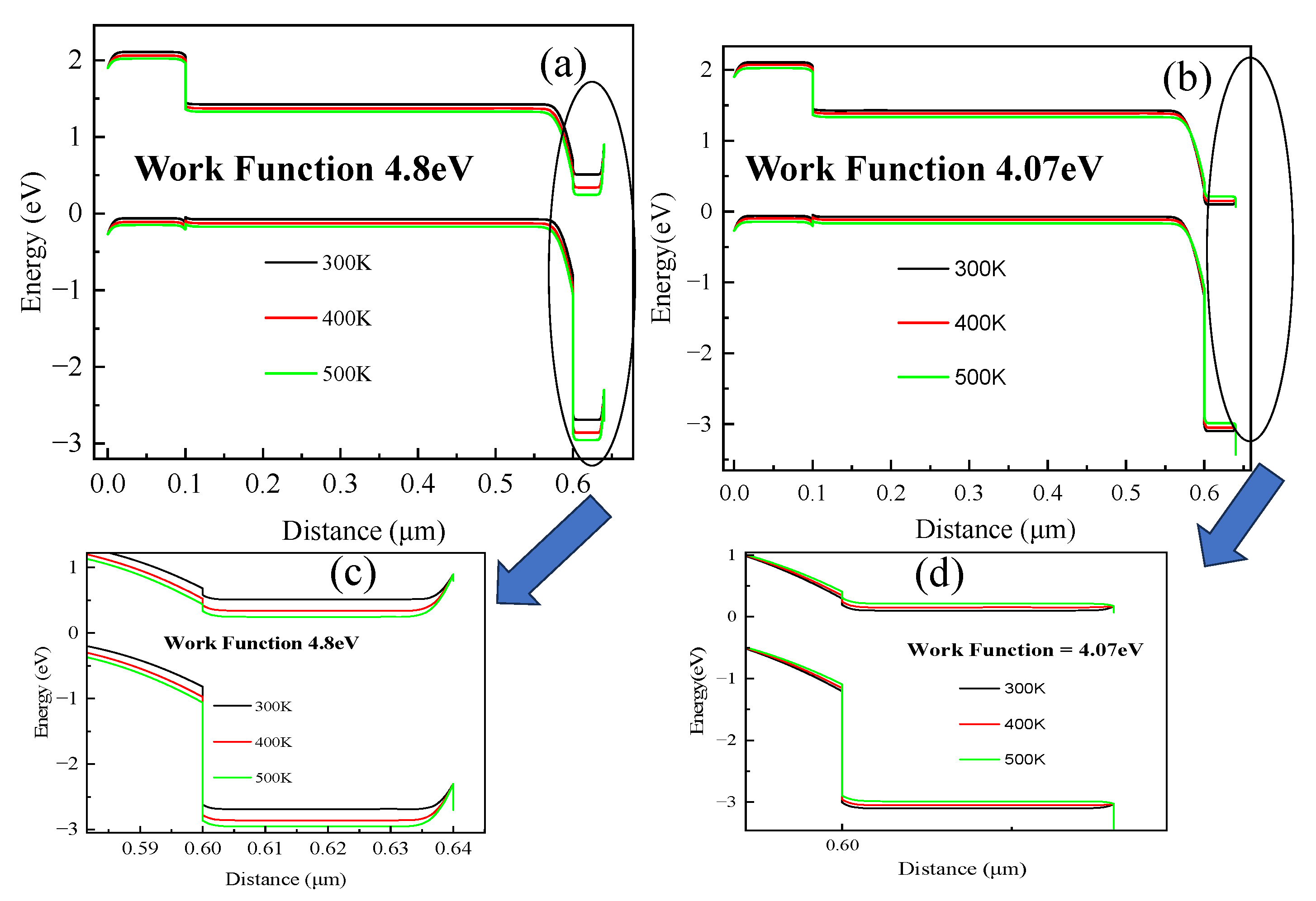
Figure 7 illustrates the temperature-dependent energy band diagrams of the BaHfSe3-based device for two representative TCO work functions (4.07 eV and 4.8 eV), simulated at 300 K, 400 K, and 500 K using SCAPS-1D. The band alignment at various interfaces—including TCO/ETL, ETL/absorber, and absorber/HTL—plays a crucial role in determining charge transport, carrier extraction, and overall device performance [45,46,47]. In the present study, different ETL and HTL materials were systematically screened to achieve optimal energy level matching with the BaHfSe3 absorber, thereby identifying the most efficient device configuration.
The present analysis focuses specifically on the TCO/ETL interface to elucidate the role of TCO work function and temperature on device behavior. Experimentally, the work function of TCOs such as ITO or FTO can be tuned without altering the material composition through surface treatments like oxygen plasma exposure, UV–ozone treatment, or controlled annealing. Therefore, the simulated variation of work function in this work is both physically meaningful and experimentally feasible.
It should be noted that in this temperature-dependent study, the TCO work function itself is not assumed to vary with temperature. Instead, it was systematically varied to examine its indirect influence on temperature-dependent photovoltaic performance. The energy band diagrams show that, with increasing temperature, all interfaces except the TCO/ETL junction exhibit nearly parallel shifts, indicating that the band edges of the ETL, absorber, and HTL layers move uniformly. Consequently, their relative alignments remain effectively unchanged, and they contribute similarly to device performance across the temperature range.
A distinct behavior is observed at the TCO/ETL interface. For the higher TCO work function (4.8 eV), the interfacial barrier height decreases with increasing temperature, as evident from Figure 6. This reduction enhances carrier extraction and results in an initial increase in both open-circuit voltage (Voc) and short-circuit current density (Jsc) at moderate temperatures. However, as the temperature continues to rise, the increase in reverse saturation current and recombination processes becomes dominant, leading to a subsequent decrease in these parameters. In contrast, for the lower TCO work function (4.07 eV), the barrier height remains nearly constant with temperature, resulting in a monotonic decrease of Voc, Jsc, and overall efficiency.
Therefore, the observed non-monotonic variation of device parameters (initial increase followed by a decrease) can be comprehensively explained by the temperature-dependent band alignment and barrier height evolution at the TCO/ETL junction, while the other interfaces remain relatively unaffected.

4. Conclusions

This study demonstrates the promising potential of lead-free chalcogenide perovskite BaHfSe3 as an efficient and environmentally stable absorber in perovskite solar cells. Through comprehensive SCAPS-1D simulations, the optimized device architecture—TCO/TiO2 (50 nm)/BaHfSe3 (500 nm)/Cu2O (100 nm)/Au—achieves excellent photovoltaic performance metrics, with a power conversion efficiency of 24.47% under standard conditions. The device performance is shown to be sensitive to absorber thickness and defect density, reinforcing the importance of material quality and controlled fabrication.
The temperature-dependent analysis reveals that the photovoltaic parameters, especially Voc, FF, and efficiency, exhibit distinct behaviors governed by the TCO work function and corresponding interface barrier height. For lower TCO work functions, efficiency and Voc decrease monotonically with temperature due to increases in saturation current driven by intrinsic carrier concentration. In contrast, higher work functions produce a non-monotonic temperature dependence, where initial efficiency improvements arise from barrier height reduction and favorable Fermi level shifts before declining at elevated temperatures.
These findings underscore the critical role of interface band alignment and defect management in optimizing device stability and performance over operational temperature ranges. Moreover, BaHfSe3, with its suitable bandgap, strong absorption, and robustness, emerges as a viable lead-free alternative to conventional hybrid perovskites, advancing the prospects of thermally stable, high-efficiency, and environmentally friendly photovoltaic technologies.

Supplementary Materials

The following supporting information can be downloaded at: https://www.mdpi.com/article/10.3390/eng6120345/s1, Figure S1: (a) Variation of Voc and Jsc (b) Variation of FF and efficiency with ETL thickness (c) Variation of Voc and Jsc (d) Variation of FF and efficiency with HTL thickness. Figure S2: (a) Simulated J–V characteristics of the BaHfSe3-based perovskite solar cell for different values of the radiative recombination constant. (b) Corresponding variation of power conversion efficiency (PCE) as a function of the radiative recombination constant, illustrating its influence on overall device performance. Figure S3: (a) Variation of Voc and Jsc with band gap (b) variation of efficiency and FF with band gap. Figure S4: Variation of PCE with variation in electron mobility.

Author Contributions

Conceptualization, B.G.; Data curation, M.M.; Formal analysis, M.M. and S.M.; Funding acquisition, N.S.; Methodology, M.M.; Project administration, B.G.; Software, M.M.; Supervision, N.S.; Writing—original draft, B.G.; Writing—review and editing, S.M. and N.S. All authors have read and agreed to the published version of the manuscript.

Funding

This research is funded by the WPI program, ARIM of MEXT (JPMXP1225NM5200), JSPS KAKENHI grant (24K01462 and 24K21720), and the Hosokawa Powder Technology Foundation (HPTF24111).

Institutional Review Board Statement

Not applicable.

Informed Consent Statement

Not applicable.

Data Availability Statement

The original contributions presented in this study are included in the article/Supplementary Material. Further inquiries can be directed to the corresponding authors.

Acknowledgments

The authors thank the Marc Burgelman, University of Gent, Belgium for the 1D SCAPS software (Version: 3.3.09). M.M thanks Arjun Mukhopadhyay for useful discussion. BG thanks Asim Guchhait and Ipsita Saha for valuable discussions.

Conflicts of Interest

The authors declare no conflicts of interest.

References

  1. Hamukwaya, S.L.; Hao, H.; Zhao, Z.; Dong, J.; Zhong, T.; Xing, J.; Hao, L.; Mashingaidze, M.M. A Review of Recent Developments in Preparation Methods for Large-Area Perovskite Solar Cells. Coatings 2022, 12, 252. [Google Scholar] [CrossRef]
  2. Afre, R.A.; Pugliese, D. Perovskite Solar Cells: A Review of the Latest Advances in Materials, Fabrication Techniques, and Stability Enhancement Strategies. Micromachines 2024, 15, 192. [Google Scholar] [CrossRef] [PubMed]
  3. Roy, P.; Ghosh, A.; Barclay, F.; Khare, A.; Cuce, E. Perovskite Solar Cells: A Review of the Recent Advances. Coatings 2022, 12, 1089. [Google Scholar] [CrossRef]
  4. Nie, R.; Dai, Y.; Wang, R.; Li, L.; Park, B.; Chu, W.; Wang, C.; Li, Z.; Chen, S.; Qiao, R. Enhanced Stability and Efficiency in Perovskite Solar Cells via Mixed-Metal Chalcohalide-Alloyed Formamidinium Lead Iodide. Nat. Commun. 2025, 16, 7343. [Google Scholar] [CrossRef]
  5. Liu, X.; Chen, L.; Yu, Y.; He, D.; Shai, X.; Zhang, S.; Zhang, Z.; Feng, J.; Yi, J.; Chen, J. Advancements of Highly Efficient Perovskite Based Tandem Solar Cells. Sci. China Mater. 2025, 68, 691–708. [Google Scholar] [CrossRef]
  6. Khenkin, M.V.; Katz, E.A.; Abate, A.; Bardizza, G.; Berry, J.J.; Brabec, C.; Brunetti, F.; Bulović, V.; Burlingame, Q.; Di Carlo, A. Consensus Statement for Stability Assessment and Reporting for Perovskite Photovoltaics Based on ISOS Procedures. Nat. Energy 2020, 5, 35–49. [Google Scholar] [CrossRef]
  7. Wei, J.; Wang, Q.; Huo, J.; Gao, F.; Gan, Z.; Zhao, Q.; Li, H. Mechanisms and Suppression of Photoinduced Degradation in Perovskite Solar Cells. Adv. Energy Mater. 2021, 11, 2002326. [Google Scholar] [CrossRef]
  8. Kore, B.P.; Jamshidi, M.; Gardner, J.M. The Impact of Moisture on the Stability and Degradation of Perovskites in Solar Cells. Mater. Adv. 2024, 5, 2200–2217. [Google Scholar] [CrossRef]
  9. Mazumdar, S.; Zhao, Y.; Zhang, X. Stability of Perovskite Solar Cells: Degradation Mechanisms and Remedies. Front. Electron. 2021, 2, 712785. [Google Scholar] [CrossRef]
  10. IEC 61646; Thin-Film Terrestrial Photovoltaic (PV) Modules—Design Qualification and Type Approval. IEC: Geneva, Switzerland, 2008.
  11. Conings, B.; Drijkoningen, J.; Gauquelin, N.; Babayigit, A.; D’Haen, J.; D’Olieslaeger, L.; Ethirajan, A.; Verbeeck, J.; Manca, J.; Mosconi, E. Intrinsic Thermal Instability of Methylammonium Lead Trihalide Perovskite. Adv. Energy Mater. 2015, 5, 1500477. [Google Scholar] [CrossRef]
  12. Habisreutinger, S.N.; Leijtens, T.; Eperon, G.E.; Stranks, S.D.; Nicholas, R.J.; Snaith, H.J. Carbon Nanotube/Polymer Composites as a Highly Stable Hole Collection Layer in Perovskite Solar Cells. Nano Lett. 2014, 14, 5561–5568. [Google Scholar] [CrossRef]
  13. Saliba, M.; Matsui, T.; Domanski, K.; Seo, J.-Y.; Ummadisingu, A.; Zakeeruddin, S.M.; Correa-Baena, J.-P.; Tress, W.R.; Abate, A.; Hagfeldt, A. Incorporation of Rubidium Cations into Perovskite Solar Cells Improves Photovoltaic Performance. Science 2016, 354, 206–209. [Google Scholar] [CrossRef]
  14. Li, G.; Su, Z.; Canil, L.; Hughes, D.; Aldamasy, M.H.; Dagar, J.; Trofimov, S.; Wang, L.; Zuo, W.; Jerónimo-Rendon, J.J. Highly Efficient Pin Perovskite Solar Cells That Endure Temperature Variations. Science 2023, 379, 399–403. [Google Scholar] [CrossRef]
  15. Schwenzer, J.A.; Rakocevic, L.; Gehlhaar, R.; Abzieher, T.; Gharibzadeh, S.; Moghadamzadeh, S.; Quintilla, A.; Richards, B.S.; Lemmer, U.; Paetzold, U.W. Temperature Variation-Induced Performance Decline of Perovskite Solar Cells. ACS Appl. Mater. Interfaces 2018, 10, 16390–16399. [Google Scholar] [CrossRef]
  16. Adjogri, S.J.; Meyer, E.L. Chalcogenide Perovskites and Perovskite-Based Chalcohalide as Photoabsorbers: A Study of Their Properties, and Potential Photovoltaic Applications. Materials 2021, 14, 7857. [Google Scholar] [CrossRef] [PubMed]
  17. Sun, Y.-Y.; Agiorgousis, M.L.; Zhang, P.; Zhang, S. Chalcogenide Perovskites for Photovoltaics. Nano Lett. 2015, 15, 581–585. [Google Scholar] [CrossRef]
  18. Vincent Mercy, E.N.; Srinivasan, D.; Marasamy, L. Emerging BaZrS3 and Ba (Zr, Ti) S3 Chalcogenide Perovskite Solar Cells: A Numerical Approach toward Device Engineering and Unlocking Efficiency. ACS Omega 2024, 9, 4359–4376. [Google Scholar] [CrossRef] [PubMed]
  19. Karthick, S.; Velumani, S.; Bouclé, J. Chalcogenide BaZrS3 Perovskite Solar Cells: A Numerical Simulation and Analysis Using SCAPS-1D. Opt Mater 2022, 126, 112250. [Google Scholar] [CrossRef]
  20. Srinivasan, D.; Rasu Chettiar, A.-D.; Vincent Mercy, E.N.; Marasamy, L. Scrutinizing the Untapped Potential of Emerging ABSe3 (A = Ca, Ba; B = Zr, Hf) Chalcogenide Perovskites Solar Cells. Sci. Rep. 2025, 15, 3454. [Google Scholar] [CrossRef]
  21. Dallas, P.; Gkini, K.; Kaltzoglou, A.; Givalou, L.; Konstantakou, M.; Orfanoudakis, S.; Boukos, N.; Sakellis, E.; Tsipas, P.; Kalafatis, A. Exploring the Potential of Powder-to-Film Processing for Proof-of-Concept BaZrS3 Perovskite Solar Cells. Mater. Today Commun. 2024, 39, 108608. [Google Scholar] [CrossRef]
  22. Bystrický, R.; Tiwari, S.K.; Hutár, P.; Sykora, M. Thermal Stability of Chalcogenide Perovskites. Inorg. Chem. 2024, 63, 12826–12838. [Google Scholar] [CrossRef]
  23. Verma, A.A.; Dwivedi, D.K.; Kumar, M. Revolutionizing Energy Band Alignment: Parabolic Grading for High-Performance BaZrS3−x Se x Chalcogenide Perovskite Solar Cells. J. Electron. Mater. 2025, 54, 10085–10099. [Google Scholar] [CrossRef]
  24. Kumar, S.; Gahlawat, D.; Kaur, J.; Rani, U.; Madan, J.; Pandey, R.; Basu, R. Temperature-Induced Variations in the Optoelectronic and Impedance Responses of Bandgap-Engineered BaZrS3 Chalcogenide Perovskite Solar Cells: A Numerical Study. J. Inorg. Organomet. Polym. Mater. 2025, 1–26. [Google Scholar] [CrossRef]
  25. Huang, L.; Zhang, D.; Bu, S.; Peng, R.; Wei, Q.; Ge, Z. Synergistic Interface Energy Band Alignment Optimization and Defect Passivation toward Efficient and Simple-structured Perovskite Solar Cell. Adv. Sci. 2020, 7, 1902656. [Google Scholar] [CrossRef]
  26. Walter, D.; Peng, J.; Weber, K.; Catchpole, K.R.; White, T.P. Performance Limitations Imposed by the TCO Heterojunction in High Efficiency Perovskite Solar Cells. Energy Environ. Sci. 2022, 15, 5202–5216. [Google Scholar] [CrossRef]
  27. Salih, M.A.; Mustafa, M.A.; Yousef, B.A.A. Developing Lead-Free Perovskite-Based Solar Cells with Planar Structure in Confined Mode Arrangement Using SCAPS-1D. Sustainability 2023, 15, 1607. [Google Scholar] [CrossRef]
  28. Samiul Islam, M.; Sobayel, K.; Al-Kahtani, A.; Islam, M.A.; Muhammad, G.; Amin, N.; Shahiduzzaman, M.; Akhtaruzzaman, M. Defect Study and Modelling of SnX3-Based Perovskite Solar Cells with SCAPS-1D. Nanomaterials 2021, 11, 1218. [Google Scholar] [CrossRef]
  29. Zyoud, S.H.; Zyoud, A.H.; Ahmed, N.M.; Abdelkader, A.F.I. Numerical Modelling Analysis for Carrier Concentration Level Optimization of CdTe Heterojunction Thin Film–Based Solar Cell with Different Non–Toxic Metal Chalcogenide Buffer Layers Replacements: Using SCAPS–1D Software. Crystals 2021, 11, 1454. [Google Scholar] [CrossRef]
  30. Hossain, M.K.; Rubel, M.H.K.; Toki, G.F.I.; Alam, I.; Rahman, M.F.; Bencherif, H. Effect of Various Electron and Hole Transport Layers on the Performance of CsPbI3-Based Perovskite Solar Cells: A Numerical Investigation in DFT, SCAPS-1D, and WxAMPS Frameworks. ACS Omega 2022, 7, 43210–43230. [Google Scholar] [CrossRef]
  31. Hossain, M.K.; Mohammed, M.K.A.; Pandey, R.; Arnab, A.A.; Rubel, M.H.K.; Hossain, K.M.; Ali, M.H.; Rahman, M.F.; Bencherif, H.; Madan, J. Numerical Analysis in DFT and SCAPS-1D on the Influence of Different Charge Transport Layers of CsPbBr3 Perovskite Solar Cells. Energy Fuels 2023, 37, 6078–6098. [Google Scholar] [CrossRef]
  32. Burgelman, M.; Nollet, P.; Degrave, S. Modelling Polycrystalline Semiconductor Solar Cells. Thin Solid. Films 2000, 361, 527–532. [Google Scholar] [CrossRef]
  33. Yuan, S.; Li, Z.; Wang, Y.; Zhao, H. Theoretical Study and Analysis of CsSnX3 (X = Cl, Br, I) All-Inorganic Perovskite Solar Cells with Different X-Site Elements. Molecules 2024, 29, 2599. [Google Scholar] [CrossRef]
  34. Hossain, M.K.; Islam, M.A.; Uddin, M.S.; Paramasivam, P.; Hamid, J.A.; Alshgari, R.A.; Mishra, V.K.; Haldhar, R. Design and Simulation of CsPb. 625Zn. 375IBr2-Based Perovskite Solar Cells with Different Charge Transport Layers for Efficiency Enhancement. Sci. Rep. 2024, 14, 3957–3979. [Google Scholar] [CrossRef]
  35. Lotfy, L.A.; Abdelfatah, M.; Sharshir, S.W.; El-Naggar, A.A.; Ismail, W.; El-Shaer, A. Numerical Simulation and Optimization of FTO/TiO2/CZTS/CuO/Au Solar Cell Using SCAPS-1D. Sci. Rep. 2025, 15, 28022. [Google Scholar] [CrossRef]
  36. Peng, C.-H.; Lin, Y.-C. SCAPS-1D Simulation of Various Hole Transport Layers’ Impact on CsPbI2Br Perovskite Solar Cells Under Indoor Low-Light Conditions. Solids 2025, 6, 31. [Google Scholar] [CrossRef]
  37. Jaykhedkar, N.; Bystrický, R.; Sykora, M.; Bucčko, T. How the Temperature and Composition Govern the Structure and Band Gap of Zr-Based Chalcogenide Perovskites: Insights from ML Accelerated AIMD. Inorg. Chem. 2023, 62, 12480–12492. [Google Scholar] [CrossRef] [PubMed]
  38. Shimul, A.I.; Ghosh, A.; Sarker, S.R.; Alturaifi, H.A. Examining the Contribution of Charge Transport Layers to Boost the Performance over 26% in Sr3PCl3 Absorber-Based Bifacial Perovskite Solar Cells. RSC Adv. 2025, 15, 7663–7681. [Google Scholar] [CrossRef] [PubMed]
  39. Sławek, A.; Starowicz, Z.; Lipiński, M. The Influence of the Thickness of Compact TiO2 Electron Transport Layer on the Performance of Planar CH3NH3PbI3 Perovskite Solar Cells. Materials 2021, 14, 3295. [Google Scholar] [CrossRef]
  40. ASTM G173-03; Standard Tables for Reference Solar Spectral Irradiances: Direct Normal and Hemispherical on a 37° Tilted Surface. ASTM International: West Conshohocken, PA, USA, 2020.
  41. Lee, H.-M.; Kim, S.-S.; Kim, H.-K. Artificially MoO3 Graded ITO Anodes for Acidic Buffer Layer Free Organic Photovoltaics. Appl. Surf. Sci. 2016, 364, 340–348. [Google Scholar] [CrossRef]
  42. Lei, H.; Qin, P.; Ke, W.; Guo, Y.; Dai, X.; Chen, Z.; Wang, H.; Li, B.; Zheng, Q.; Fang, G. Performance Enhancement of Polymer Solar Cells with High Work Function CuS Modified ITO as Anodes. Org. Electron. 2015, 22, 173–179. [Google Scholar] [CrossRef]
  43. Gassenbauer, Y.; Schafranek, R.; Klein, A.; Zafeiratos, S.; Hävecker, M.; Knop-Gericke, A.; Schlögl, R. Surface States, Surface Potentials, and Segregation at Surfaces of Tin-Doped In2O3. Phys. Rev. B 2006, 73, 245312. [Google Scholar] [CrossRef]
  44. Kumar, S.; Bharti, P.; Pradhan, B. Performance Optimization of Efficient PbS Quantum Dots Solar Cells through Numerical Simulation. Sci. Rep. 2023, 13, 10511. [Google Scholar] [CrossRef] [PubMed]
  45. Zhao, P.; Lin, Z.; Wang, J.; Yue, M.; Su, J.; Zhang, J.; Chang, J.; Hao, Y. Numerical Simulation of Planar Heterojunction Perovskite Solar Cells Based on SnO2 Electron Transport Layer. ACS Appl. Energy Mater. 2019, 2, 4504–4512. [Google Scholar] [CrossRef]
  46. Raj, A.; Kumar, M.; Singh, D.V.; Singh, B.; Dwivedi, D.K.; Anshul, A. Physical Parameter Optimization and Band Alignment Approach for Efficiency Improvement in Cs2AgBiBr6 Based Lead-Free Perovskite Solar Cells. Sci. Rep. 2025, 15, 32868. [Google Scholar] [CrossRef] [PubMed]
  47. Saha, N.; Brunetti, G.; Di Carlo, A.; Ciminelli, C. Efficiency Boost of Perovskite Solar Cell in Homojunction Configuration through Tailored Band Alignment and p–n Doping Profile. J. Phys. Energy 2025, 7, 045009. [Google Scholar] [CrossRef]
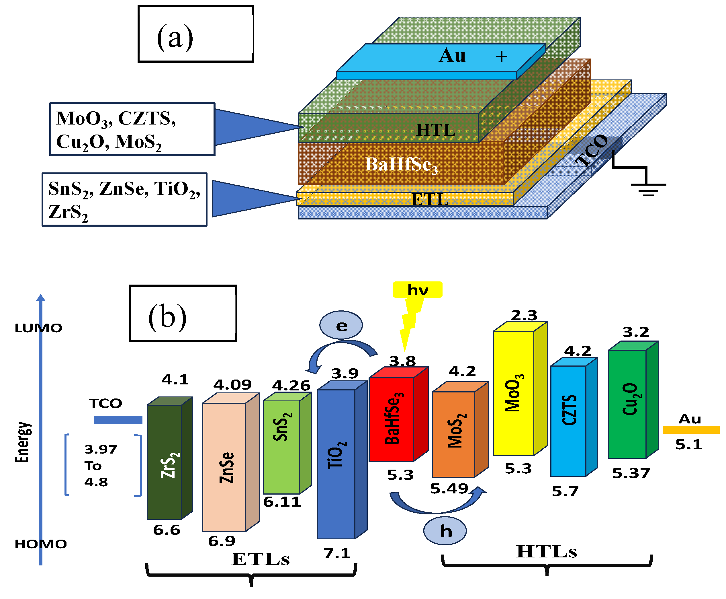
Figure 1. (a) Proposed n-i-p structure of the PSC with different layers. (b) Energy band diagram of the PSC structure (combined) with bandgap denotation for absorber and different possible charge transport layers.
Eng 06 00345 g001
Figure 2. Efficiencies with different HTL and ETL combination.
Eng 06 00345 g002
Figure 3. Variation of (a) short-circuit current density, open-circuit voltage, (b) fill factor, and efficiency with absorber layer thickness.
Eng 06 00345 g003
Figure 4. Variation of power conversion efficiency (PCE) with total defect density for different absorber layer thicknesses, as specified in the legend.
Eng 06 00345 g004
Figure 5. Variation of (a) open-circuit voltage (Voc), and short-circuit current density (Jsc), (b) fill factor (FF), and power conversion efficiency (PCE) with different TCO work functions. Band diagram (c) before contact band diagram (d) after contact with TCO of WF 3.97 eV and 4.8 eV.
Eng 06 00345 g005
Figure 6. Variation of (a) open-circuit voltage (Voc), (b) short-circuit current density (Jsc), (c) fill factor (FF), and (d) power conversion efficiency (PCE) with temperature for six different TCO work functions, as specified in the legend.
Eng 06 00345 g006
Figure 7. Energy band diagrams of the BaHfSe3-based device at different temperatures for (a) TCO work function of 4.80 eV and (b) TCO work function of 4.07 eV. Panels (c,d) show the corresponding zoomed-in views of the TCO/ETL interface regions for (a,b), respectively, highlighting the variation in interface barrier alignment with temperature.
Eng 06 00345 g007
Disclaimer/Publisher’s Note: The statements, opinions and data contained in all publications are solely those of the individual author(s) and contributor(s) and not of MDPI and/or the editor(s). MDPI and/or the editor(s) disclaim responsibility for any injury to people or property resulting from any ideas, methods, instructions or products referred to in the content.