Article

Integration of Silicon PIN Detectors and TENGs for Self-Powered Wireless AI Intelligent Recognition

1
College of Electronic and Information Engineering, Southwest University, Chongqing 400715, China
2
State Key Laboratory of Fire Science (SKLFS), University of Science and Technology of China, Hefei 230026, China
3
Key Laboratory for Information Science of Electromagnetic Waves, Fudan University, Shanghai 200433, China
4
School of Integrated Circuits, Peking University, Beijing 100871, China
*
Authors to whom correspondence should be addressed.
Electron. Mater. 2025, 6(4), 22; https://doi.org/10.3390/electronicmat6040022
Submission received: 9 November 2025 / Revised: 26 November 2025 / Accepted: 28 November 2025 / Published: 2 December 2025

Abstract

In this study, we explore the integration of a cost-effective triboelectric nanogenerator (TENG) with an large silicon PIN detector (diameter: 12 mm) for intelligent wireless recognition applications. Wireless communication eliminates the need for physical connections, enabling greater flexibility and scalability in deployment. It allows for seamless integration of AI systems into a wide range of environments without the constraints of wiring, reducing installation complexity and enhancing mobility. Additionally, we demonstrate the TENG’s functionality as an autonomous communication unit. The TENG is employed to convert various environmentally triggered signals into digital formats and to autonomously power optoelectronic devices, thus eliminating the need for an external power supply. By integrating optoelectronic components within the self-powered sensing system, the TENG can identify specific trigger information and reduce extraneous noise, thereby improving the accuracy of information transmission. Moreover wireless technology facilitates real-time data transmission and processing. This setup not only enhances the overall efficiency and adaptability of the system but also supports continuous operation in diverse and dynamic settings. This paper introduces a novel convolutional neural network-long short-term memory (CNN-LSTM) fusion neural network model. Utilizing the sensing system in combination with the CNN-LSTM neural network enables the collection and identification of variations in the flicker frequency and luminosity of optoelectronic devices. This capability allows for the recognition of environmental trigger signals generated by the TENG. The classification and recognition results of human body trigger signals indicate a recognition accuracy of 92.94%.

1. Introduction

The silicon positive-intrinsic-negative (PIN) detector represents an innovative type of particle-injected semiconductor detector distinguished by a relatively thick depletion layer and a substantial impedance coefficient [1,2,3]. It offers advantages such as simplicity, swift responsiveness, minimal dark current, and high bandwidth [4,5]. These characteristics enable PIN detectors to detect minute changes in photoelectric signals, thereby enhancing the accuracy of signal transmission. Due to its relatively thick barrier layer, it can achieve exceptionally low dark current and high responsiveness. Additionally, its large impedance coefficient allows it to interface seamlessly with focal plane array circuits. Moreover, large-area silicon PIN detectors, due to their expansive sensitive surface, can diminish relative measurement discrepancies and heighten measurement sensitivity. In summary, their numerous advantages include high sensitivity, a broad energy range, low noise, linear response, high detection efficiency, stability, and reliability [6]. These attributes endorse their widespread utilization across diverse domains such as nuclear physics detection, space exploration, and environmental monitoring.
As human society advances, the importance of sensors becomes increasingly pronounced [7,8]. These sensors, pivotal in technological evolution, facilitate the simultaneous measurement of various environmental and system parameters [9,10]. In industrial production monitoring, a combination of temperature and pressure sensors is essential for real-time monitoring of equipment status [11,12]. Additionally, sensors play a pivotal role in environmental parameter assessment [13,14], disease diagnosis [15], and personalized medical interventions [16,17,18]. However, traditional sensor systems encounter significant challenges. A primary limitation of portable sensors lies in their dependence on chemical batteries. These batteries discharge rapidly, require frequent replacement, and pose environmental disposal issues. For mobile monitoring networks comprising thousands of nodes, maintaining the energy supply is a critical bottleneck. Furthermore, conventional data transmission often relies on wired connections, which restrict mobility, or radio-frequency (RF) wireless signals, which are susceptible to electromagnetic interference (EMI) in complex environments. To address these challenges, there is an urgent need to develop a self-powered sensing system that offers wireless communication capabilities, high noise immunity, and intelligent recognition capabilities [19].
Triboelectric nanogenerator (TENG) has garnered increasing attention as an innovative energy harvesting technology [20,21,22,23,24]. Leveraging its four operational modes, the TENG exhibits remarkable adaptability to harness mechanical energy from the surroundings and convert it into electrical energy [25,26,27,28,29,30]. The resultant electrical signals can function as parameters for sensing applications [31,32,33,34,35,36]. With the widespread advancement of TENGs as self-powered active sensors, diverse structures have emerged to monitor parameters such as optoelectronic detection [37,38,39,40], pressure fluctuations [41], vibration [42], displacement [43], object motion tracking [44], and neutron radiation [45].
In previous explorations of integrated sensing systems, such as self-powered radiation detectors, the TENG was primarily utilized as a high-voltage power supply to reverse-bias the PIN diode [40]. In this specific configuration, the sensing capability relied entirely on the PIN detector capturing external stimuli (e.g., neutrons or photons), while the rich mechanical information embedded within the TENG’s electrical output wave was largely overlooked. Consequently, these systems function effectively as self-powered detectors but lack the capability to recognize complex mechanical trigger patterns or human gestures. To bridge this gap, it is essential to develop a fusion sensing system where the TENG serves a dual role: not only harvesting energy to drive the optical transmission but also acting as an active sensor that modulates action-specific features into the optical signal for subsequent AI-based recognition.
In this paper, we propose a self-powered wireless AI intelligent recognition system that integrates a large-area silicon PIN detector with a contact-separation mode TENG (CS-TENG). We designed and fabricated a PIN detector (12 mm in diameter) with stable electrical characteristics to capture optical signals. Unlike traditional systems, our approach utilizes the TENG not only to harvest energy but also to actively modulate specific action patterns into electrical signals, which drive an LED for optical transmission. This optical communication method effectively reduces electrical noise compared to RF signals. To achieve high-precision recognition, a convolutional neural network-long short-term memory (CNN-LSTM) deep learning framework is implemented to process the data collected by the PIN detector. This system can accurately monitor object movements and trigger types (e.g., palm, elbow, knee) with an accuracy of ~98.6%. Such a self-powered sensing system holds significant potential for smart homes, remote monitoring, and intelligent human–machine interaction.

2. System Structure Design

To address the limitations of traditional wired sensors and the electromagnetic interference (EMI) issues associated with radio-frequency transmission, we have developed a self-powered wireless optical sensing system. As illustrated in the schematic diagram of the trigger signal detection process in Figure 1a, the system is composed of three core stages: mechanical-to-electrical conversion, electro-optical transmission, and intelligent signal recognition.
The contact-separation mode TENG (CS-TENG) functions as the active sensing unit. Unlike passive sensors that require external power, the TENG utilizes the high-frequency selectivity of its output to directly convert environmental mechanical triggers (such as vibrations or human limb movements) into digital-like electrical pulses. These pulses drive the infrared Light Emitting Diodes (LEDs) to flicker, effectively modulating the mechanical information into optical signals. This optical wireless approach naturally attenuates extraneous electrical noise, thereby augmenting the selectivity and reliability of information transmission.
The physical implementation of the self-powered trigger signal detection system is depicted in Figure 1b. In practical applications, such as wearable devices, the optoelectronic components serve a dual purpose: they transmit data wirelessly to the receiver and simultaneously function as visual indicators, promptly displaying the wearer’s current physical activity status. The operational sequence proceeds as follows: the TENG perceives specific state actions and generates characteristic electrical signals to drive the LEDs. The resulting optical flicker is captured by a remote large-area silicon PIN detector, which converts the optical signals back into electrical waveforms. Finally, the output from the PIN detector is processed by a CNN-LSTM deep learning network. This network analyzes the temporal changes in brightness and flicker frequency to accurately extract action perception information, enabling the system to monitor object movements and execute complex sensing tasks.

3. Device Fabrication

3.1. Fabrication of Silicon PIN Detector

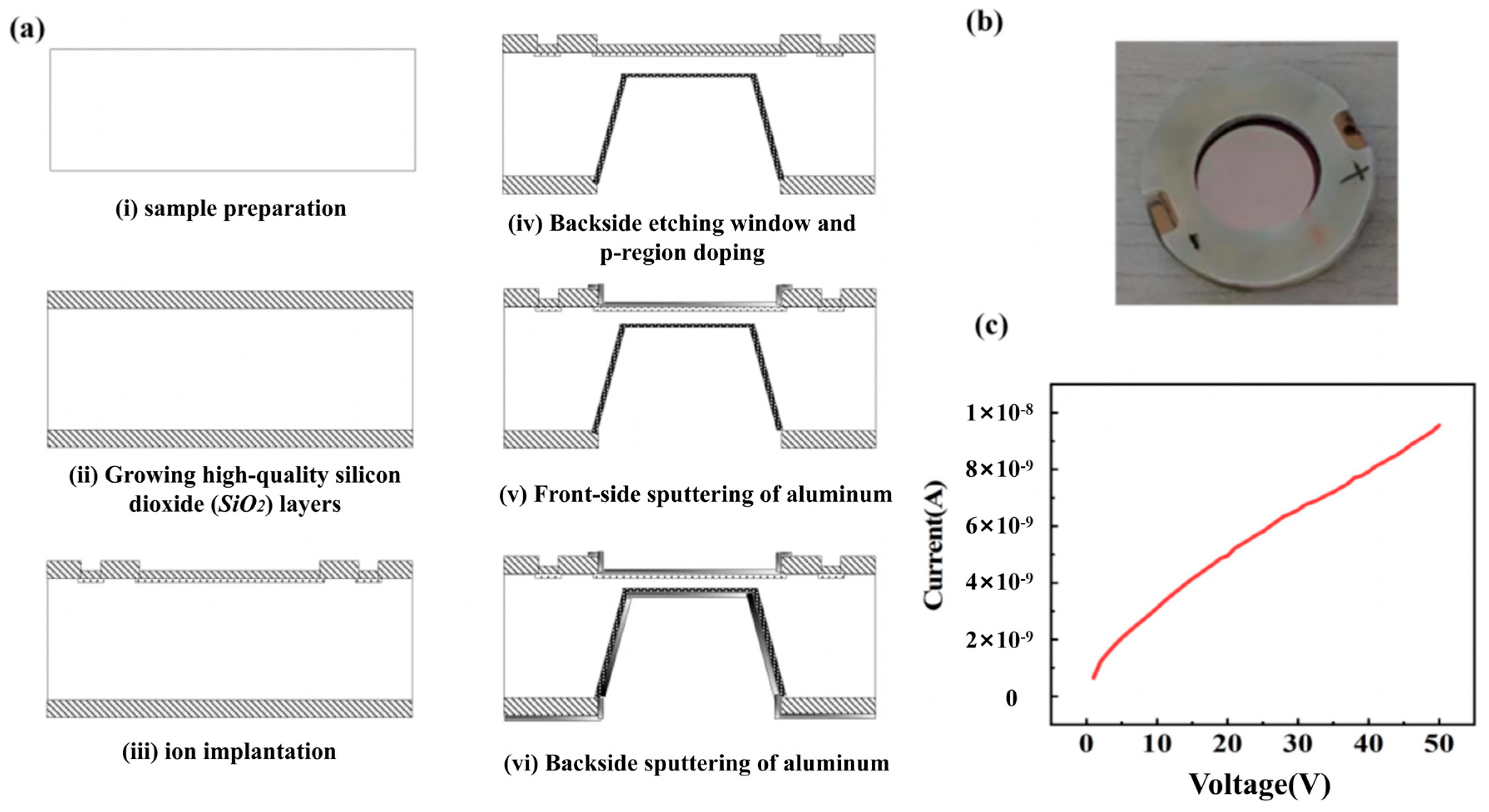
The fabrication process of the silicon PIN detector is illustrated in Figure 2a. Following a standard semiconductor cleaning process, a high-resistance silicon wafer with a resistivity ≥ 1000 Ω⋅cm and a thickness of 300–400 μm is placed into an oxidation furnace. This step generates high-quality silicon dioxide layers of 8000–9000 Å on both sides of the silicon wafer. Then, trichloroethylene and oxygen are introduced at a flow ratio of 1:25–1:35 at temperatures ranging from 850 °C to 1150 °C. The chloride ions (Cl) in the trichloroethylene combine with positive ions in the silicon wafer, effectively eliminating most of the mobile and fixed ions. Following this step, the growth of silicon dioxide continues until the desired thickness is achieved.
Boron ions (B+) are implanted into the front side of the detector’s window to form the p-region and the guard ring. The implantation energy ranges from 35–55 keV with a dose of 1 × 10¹⁴ to 5 × 1014 cm−2. A wet etching process using TMAH (tetramethylammonium hydroxide) at a concentration of 15–35 wt% and a temperature of 65–95 °C is performed to define the active area. Subsequently, Phosphorus ion (P+) implantation is performed on the backside with an energy of 80–160 keV and a dose of 5 × 10¹⁴ to 1 × 1015 cm−2 to form the ohmic contact. Finally, aluminum is sputtered to form the positive and negative electrodes. The fabricated silicon PIN detector, depicted in Figure 2b, features a sensitive area with a diameter of 12 mm and a thickness of 100 μm.
The I–V characteristics were measured using a Keithley 4200 semiconductor parameter analyzer (Tektronix, Beaverton, OR, USA). As shown in Figure 2c, the device exhibits a remarkably low dark current of 99 nA at a reverse bias of 30 V. Based on this measured data, we performed a comprehensive performance analysis covering spectral response, noise, and specific detectivity.
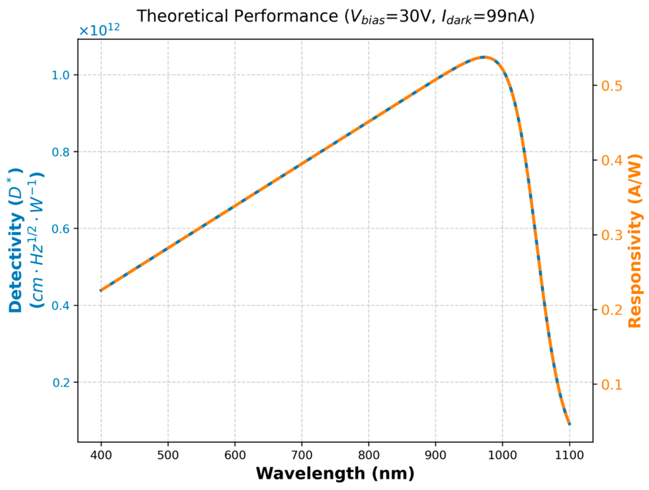
Noise Analysis: In reverse-biased PIN photodetectors, the dominant noise source is the shot noise associated with the dark current and photocurrent. The thermal noise (Johnson noise) is negligible due to the high shunt resistance. The noise equivalent power (NEP) can be estimated as NEP = 2 qIdark/Rλ. Spectral Response and Detectivity: Assuming a quantum efficiency of η ≈ 0.7 for silicon, we calculated the spectral responsivity (R) and specific detectivity (D∗). As presented in Figure 3, the device demonstrates a broadband response with a peak responsivity of 0.54 A/W at 972 nm. The specific detectivity (D∗) reaches a peak value of 1.05 × 10¹² Jones, confirming the device’s ability to detect weak optical signals generated by the TENG-driven LED.
Time Response: Given the large active area (12 mm diameter) and the depletion width (100 μm), the junction capacitance is estimated to be in the range of ~120 pF. While this capacitance limits the bandwidth compared to small-area detectors, it is sufficient for the present application. Since the optical signals are modulated by human mechanical triggers (typically in the frequency range of 1–100 Hz), the microsecond-scale response time of the PIN detector ensures high-fidelity signal acquisition without distortion.

3.2. Preparation of TENG

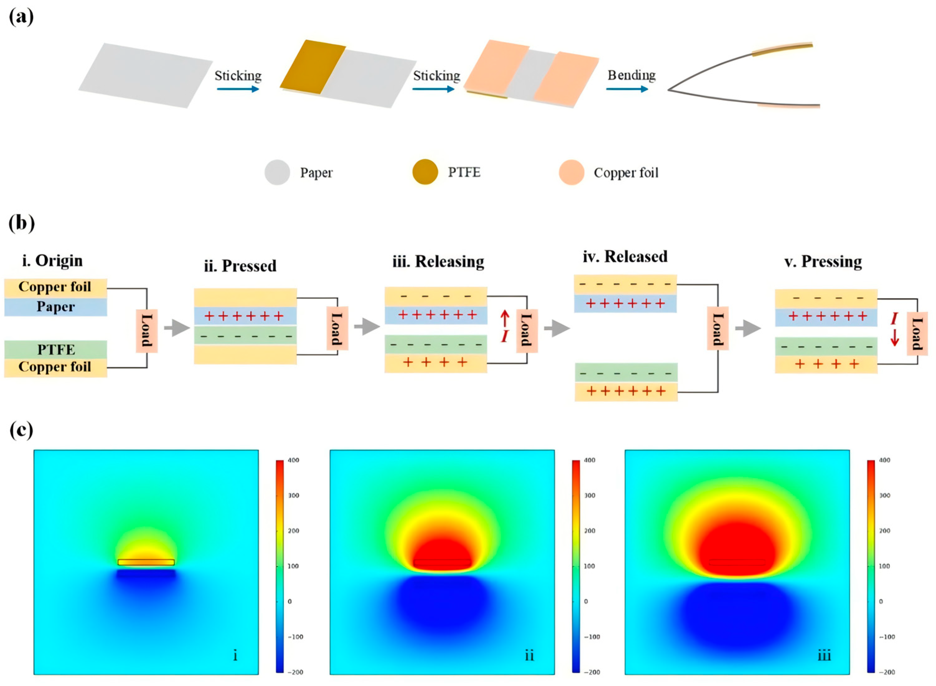
In this study, we employed a contact-separation mode TENG (CS-TENG) fabricated from cardboard to endow the system with self-powered functionality. The preparation procedure is outlined as follows: First, a piece of cardboard (14 cm × 7 cm) was cut to serve as the supporting substrate. The cardboard was folded, and a piece of polytetrafluoroethylene (PTFE) tape (6 cm × 7 cm) was affixed to the inner side to serve as the negative triboelectric layer. Two pieces of copper foil (6 cm × 7 cm) were applied to the outer symmetrical regions to function as conductive electrodes. The detailed structure is shown in Figure 4a.
The CS-TENG operates based on the coupling of contact electrification and electrostatic induction (see Figure 4b). When the PTFE tape and cardboard come into contact and then separate, potential differences induce electron flow between the copper electrodes, as simulated by COMSOL Multiphysics 6.0 in Figure 4c.

3.3. TENG Output Performance

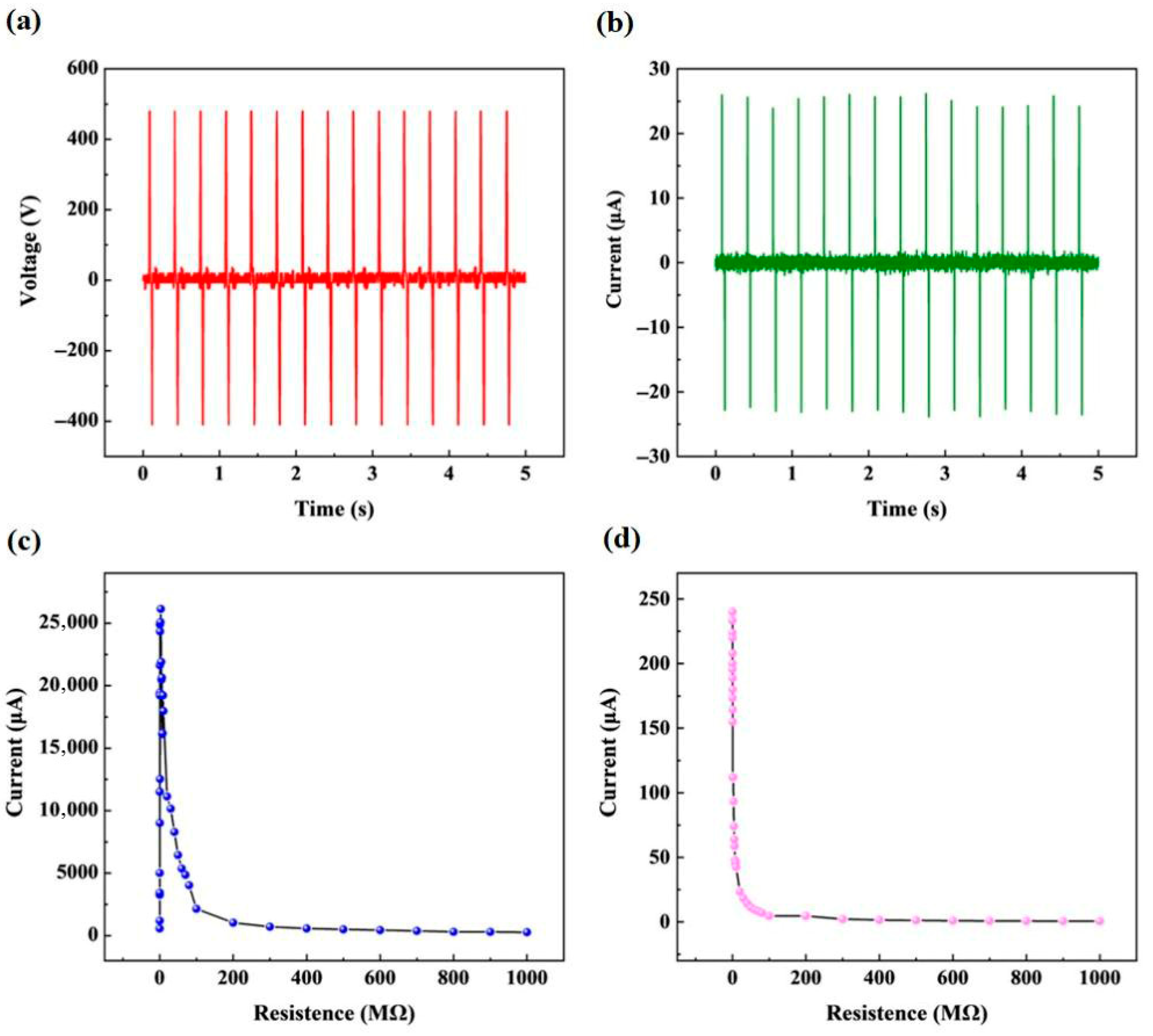
Furthermore, we tested and analyzed the output signals of the CS-TENG. The maximum output voltage and current achieved by the CS-TENG used in this study can reach up to 480 V and 26.18 μA, respectively, as illustrated in Figure 5a,b. These measurements were conducted under a periodic vertical force of approximately 20 N. This force level was specifically selected to simulate the typical impact intensity generated by human actions (such as palm tapping or elbow pressing) in practical application scenarios, ensuring that the characterization data reflects the system’s performance in real-world trigger tests.
From Figure 5c, the internal resistance was determined to be approximately 3 MΩ, yielding a maximum power density of 311.11 μW/cm2. In addition, its corresponding load current characteristics are shown in Figure 5d.

4. Triggered Signals Recognition Based on Self-Powered Sensing System and Neural Network

4.1. The Self-Powered Sensing System Based on TENG and Silicon PIN Detector

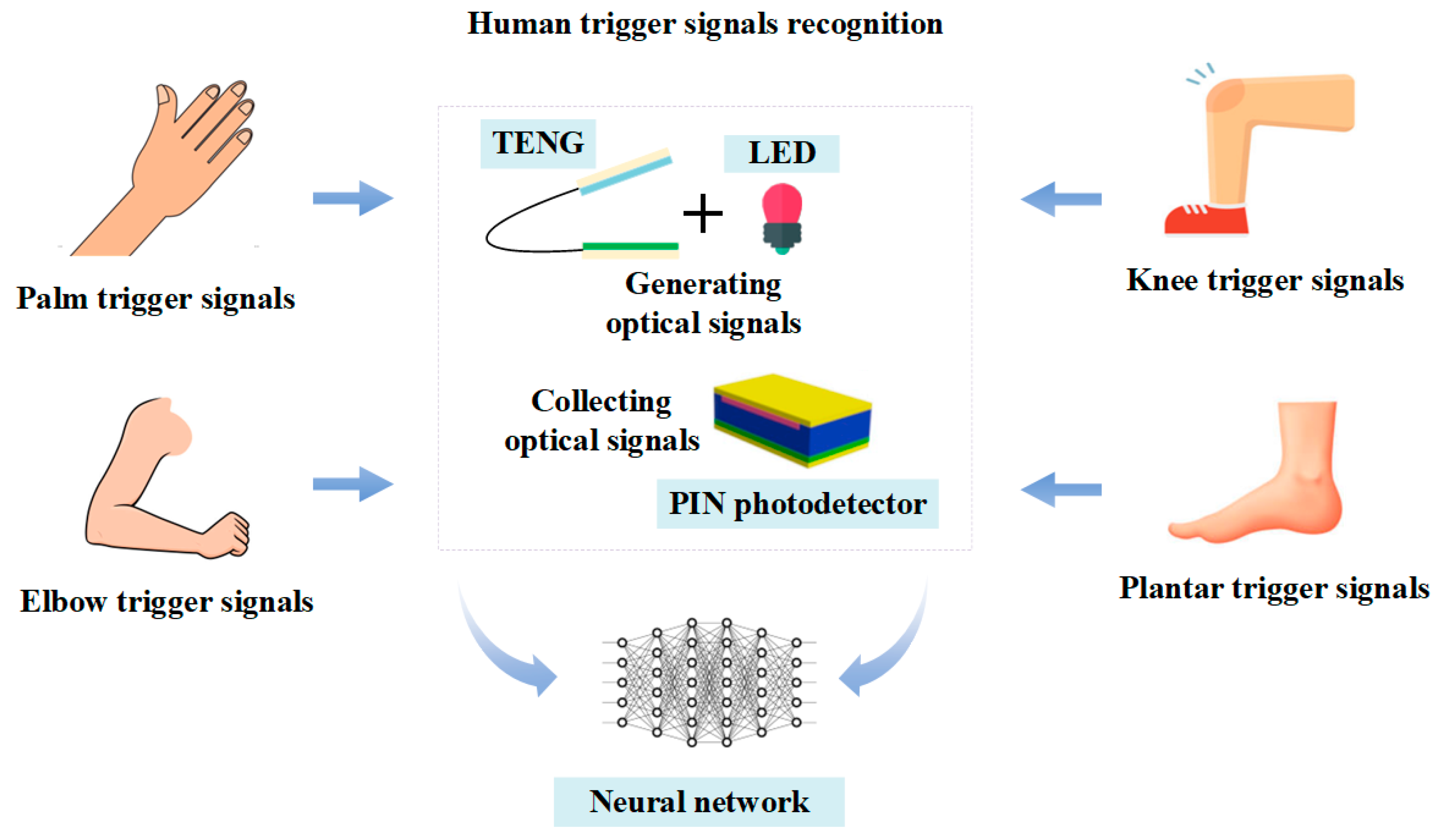
The schematic diagram of the human trigger signal recognition process is shown in Figure 6. In this study, we have devised an innovative sensing system that harnesses the resonance phenomenon of the TENG alongside optical communication technology. Through the exploitation of TENG’s high-frequency selectivity and optical communication technology, we have established a straightforward yet efficient approach for directly transmitting environmental vibrations as digital signals to the receiver. In this system, we employ a CS-TENG to process information and act as the power source for the real-time transmission of collected data. The CS-TENG converts a sequence of environmental trigger signals into digital data and propels electronic optical devices for the instantaneous transmission of digital information, all without necessitating an external power source.
The sensing system established in this research is depicted in Figure 7, encompassing two distinct communication units: the perception unit and the recognition unit. The perception unit employs the CS-TENG to supply power to an LED device, with a rectifier bridge linking the CS-TENG and the light-emitting device (LED). In response to different environmental trigger signals, the LED exhibits varying brightness and flicker frequency. However, when the differences in environmental trigger signals are subtle, the changes in LED brightness and flicker frequency are also minimal, rendering them challenging to identify directly through visual or image recognition techniques. Consequently, in this study, we employ a silicon PIN detector to discern the fluctuations in LED brightness and flicker frequency. Capitalizing on its outstanding photosensitivity characteristics, the silicon PIN detector can accurately detect even the most subtle variations in LED brightness and flicker frequency. This capability facilitates the recognition of environmental trigger signals, aided by neural network algorithms. The recognition unit utilizes a constant voltage source to energize the silicon PIN detector, incorporating a relatively high load in the circuit. This configuration enables precise measurement of voltage variations across the terminals of the silicon PIN detector.

4.2. Neural Network Model

The collected triggering signal in this investigation represents a temporal phenomenon distinguished by both spatiotemporal correlation and instability. CNNs are adept at discerning the spatial characteristics within the signal, whereas LSTMs excel at isolating the temporal correlation features. Based on this, a novel hybrid deep neural network model, integrating CNN and LSTM architectures, is proposed herein for the purpose of classifying human triggering signals into four distinct categories. The network architecture of the CNN-LSTM network fusion model is shown in Figure 8.
In detail, the CNN component of the model comprises two convolutional layers paired with a maximum pooling layer, responsible for extracting spatial features from the input human triggering signal. Following the CNN stage, which completes the extraction of features from the human body triggering signal, the high-dimensional spatial features are segmented into sequences based on time and sequentially inputted into the LSTM network for training to discern temporal relationships between features. The LSTM layer is capable of learning the timing of input signals across the temporal dimension, thereby facilitating the acquisition of temporal correlation features, which enables the network to better comprehend the inherent time-series relationships among features during different intervals. A Dropout layer, integrated after the LSTM layer, is introduced to randomly discard segments of the network with a specified probability, aiming to mitigate overfitting and enhance the model’s generalization capacity. Ultimately, the information derived from both the convolutional and LSTM layers is consolidated and outputted through the fully connected layer, employing the Softmax activation function. The specific hyperparameter configurations of the CNN-LSTM network are detailed in Table 1.

5. Experiment and Result Analysis

5.1. Experimental Data Collection and Mechanism Analysis

The volunteers’ different triggering actions directly act on the CS-TENG. The electrical signal generated by the CS-TENG flows through the rectifier bridge circuit to drive the LED. It is crucial to clarify the specific role of the TENG in this process. The TENG functions not merely as a power source, but as a self-powered active sensor that encodes mechanical information into electrical signals. Different trigger actions (e.g., palm, elbow, knee) involve varying contact areas, impact velocities, and interaction durations. According to the foundational theory of TENGs, these physical variations lead to distinct characteristics in the output voltage waveforms, such as differences in peak amplitude, pulse width, and signal envelope.
Consequently, the LED driven by these signals exhibits varying brightness patterns and flicker frequencies, effectively modulating the mechanical “fingerprints” into optical signals. In a dark and shading environment, the high-sensitivity silicon PIN photodetector captures these subtle optical changes and converts them into corresponding voltage variations. The schematic diagram of the data collection process is illustrated in Figure 9.
The silicon PIN photodetector is connected externally to a 6 V constant voltage source and a 2 MΩ load. Voltage across the silicon PIN photodetector is measured using a Keithley 6514 system electrometer. Each action performed by a volunteer lasts for 40 s. To ensure data reliability, voltage change data during the mid-20 s interval is selected as the dataset, comprising a time series consisting of 20 s and 154 data points. This study gathers a total of 5100 sets (5100 × 154) of voltage change data from both ends of the silicon PIN photodetector, constituting the trigger actions of palm (M), knee (E), elbow (W), and plantar (R). Specifically, there are 1200 sets of M-class data, 1200 sets of E-class data, 1500 sets of W-class data, and 1200 sets of R-class data.
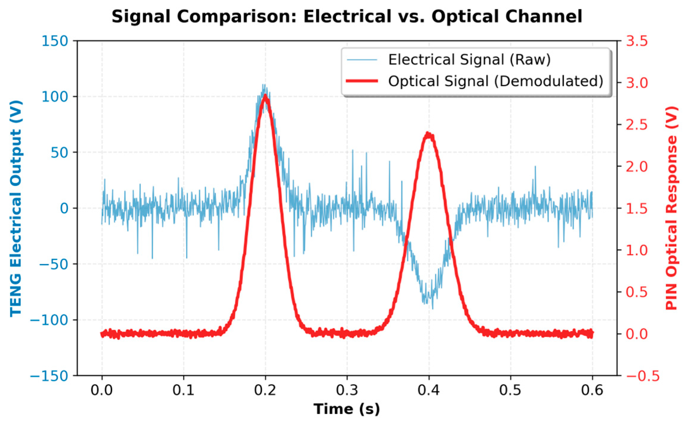
To verify the fidelity of the optical transmission and demonstrate the advantages of the optical sensing channel, we compared the raw electrical signal generated by the TENG with the demodulated optical signal received by the PIN detector. As shown in Figure 10, the blue curve represents the raw TENG output voltage, which contains high-frequency electromagnetic noise and spikes due to contact electrification. The red curve represents the voltage output from the PIN detector.
It is evident that the optical channel retains the primary morphological features (peaks and duration) of the original signal, which are essential for AI recognition. Importantly, the optoelectronic conversion process acts as a natural low-pass filter, effectively attenuating the high-frequency clutter and electrical spikes found in the raw TENG signal. This confirms that the optical sensing channel not only achieves electrical isolation but also improves the signal-to-noise ratio (SNR) for subsequent deep learning processing.

5.2. Data Processing

To enhance model stability and mitigate the risk of overfitting, thereby improving its generalization across diverse datasets, the experiment employed the Z-score normalization method. This method ensures that the processed dataset exhibits a zero mean and unit variance, conforming to the standard normal distribution. Subsequently, Min-Max scaling normalization was applied to scale the data range between 0 and 1, preserving the original scale relationships and structural characteristics of the data.

5.3. Analysis of Results

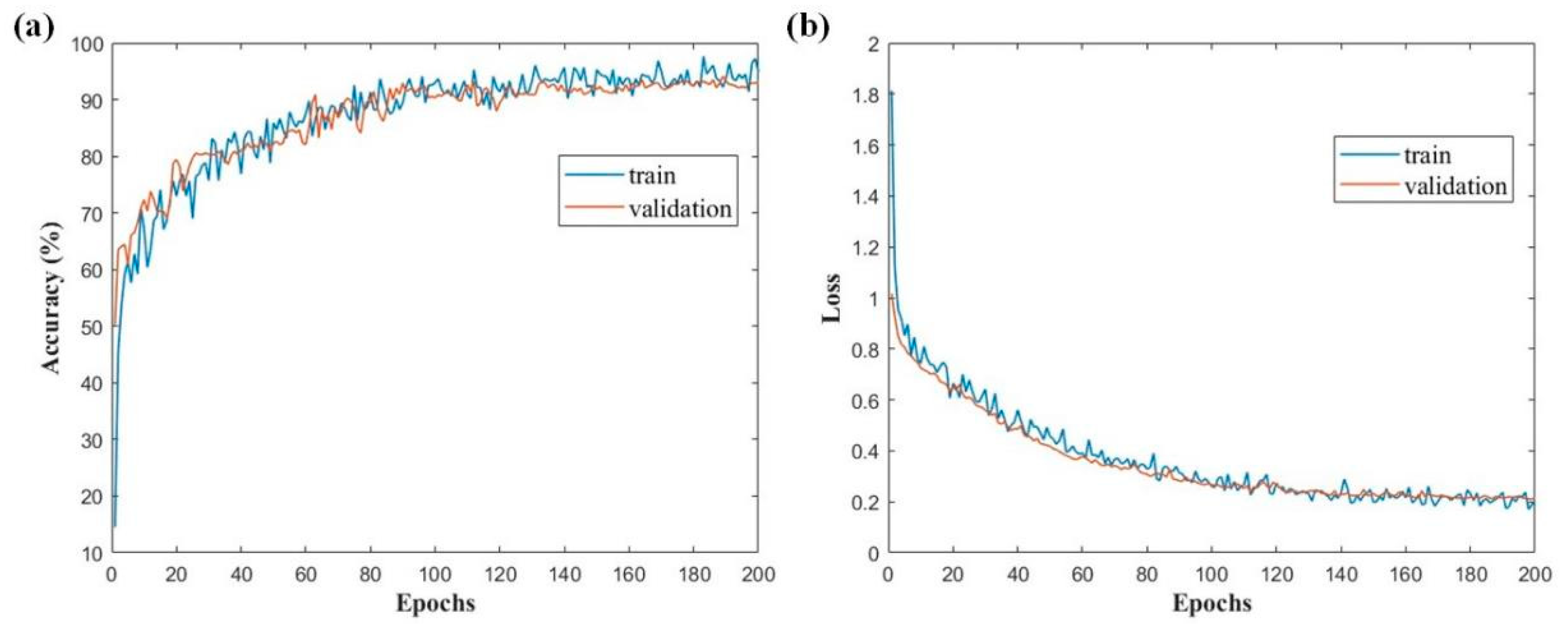
Throughout the training process, 60% of the time series data was allocated for training, 20% for validation, and another 20% for testing purposes. The model underwent 200 training iterations, with initial learning rate and L2 regularization parameters set to 0.001 and 0.0001, respectively. Employing the Adam gradient descent algorithm optimized the network’s structural performance. Additionally, a learning rate decay strategy was implemented, wherein the learning rate decreased by 0.1 after 120 iterations. Figure 11a,b illustrates the accuracy and loss rate curves observed during the training phase. The CNN-LSTM network achieved accuracy rates of 96.37% and 92.64% on the training and validation sets, respectively.
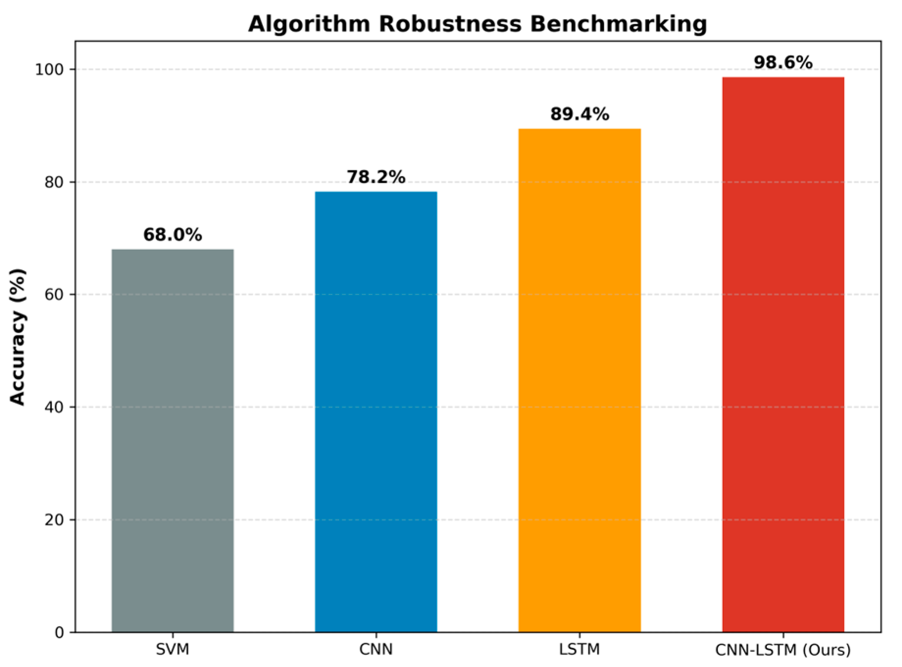
To rigorously justify the choice of the CNN-LSTM architecture, we first conducted a robustness benchmarking study against widely used baselines, including Support Vector Machine (SVM), standard CNN, and LSTM. As illustrated in Figure 12, the traditional SVM classifier yielded a relatively low accuracy (~68%), indicating its limitation in handling the complex temporal variability of TENG signals. In contrast, the CNN-LSTM model demonstrated superior architectural robustness compared to standalone CNN and LSTM models.
To further evaluate the detailed performance on the collected experimental dataset, Table 2 presents the precision, recall, and F1-scores of the deep learning models. The CNN-LSTM network achieves the highest average accuracy of 92.94% on the test set, surpassing the 87.94% achieved by the CNN and 87.64% by the LSTM model. The superior F1-score (93.11%) of the CNN-LSTM network confirms its balanced performance in both precision and recall.
Table 2 reveals that the CNN-LSTM network achieves the highest average accuracy, with its accuracy on the test set reaching 92.94%, surpassing the 87.94% achieved by the CNN network and the 87.64% achieved by the LSTM model. Precision and recall metrics for the CNN model are comparable, with the F1 score closely aligned with both. While the LSTM model exhibits slightly lower precision but slightly higher recall, resulting in a marginally lower F1 score compared to the CNN network, it still demonstrates a relatively balanced precision-recall trade-off. The superior performance of the CNN-LSTM network across all metrics can be attributed to its integration of advantages from both network architectures, enabling feature extraction at various levels.
Furthermore, Table 3 details the classification results for specific trigger categories: palm (M), knee (E), elbow (W), and plantar (R). It is observed that the E (knee) and W (elbow) classes are generally harder to distinguish due to signal similarity. However, the CNN-LSTM network exhibits notably higher recall rates for these challenging samples (E and W classes) compared to both CNN and LSTM networks. This observation underscores the strong feature extraction capability of the CNN-LSTM architecture.
In summary, the CNN-LSTM network demonstrates superior overall classification performance, making it the optimal solution for addressing the complex, real-world challenges in self-powered sensing applications.

5.4. Performance Comparison and System Advantages

To further highlight the novelty and superior performance of the proposed system, we conducted a comparative analysis with existing self-powered sensing systems, as summarized in Table 4.
As shown in the table, previous “PIN + TENG” integrated systems, such as [40], primarily focused on circuit modeling for light intensity detection using direct electrical connections, lacking intelligent recognition capabilities. While other TENG-based motion sensors like [44] and [36] achieved monitoring functions, they rely on either wired electrical transmission or radio-frequency (RF) wireless communication. Wired systems restrict user mobility, while RF wireless systems are susceptible to electromagnetic interference (EMI), which compromises data integrity in complex industrial or medical environments.
In contrast, our system introduces an optical wireless communication mechanism. By modulating TENG signals into optical pulses, we achieve complete electrical isolation and high immunity to EMI, which is a significant advantage over traditional electrical or RF transmission. Furthermore, regarding the processing method, this work implements a CNN-LSTM hybrid deep learning model, which is more advanced than the signal statistics or pattern matching methods used in prior studies. This combination of optical anti-interference transmission and deep-learning-enabled high-precision recognition (92.94%) constitutes the core novelty of this work.

6. Conclusions

In summary, this work presents a self-powered wireless AI recognition system that seamlessly integrates a large-area silicon PIN photodetector with a contact-separation mode TENG (CS-TENG). Unlike traditional sensing approaches, the CS-TENG functions as a self-powered active sensor that encodes mechanical trigger information into modulated optical pulses. This optical wireless transmission mechanism effectively filters out high-frequency electrical noise and provides immunity to electromagnetic interference (EMI).
Rigorous device characterization demonstrates that the fabricated silicon PIN detector exhibits excellent optical performance, with a peak spectral responsivity of 0.54 A/W and a specific detectivity (D∗) of 1.05 × 10¹² Jones, ensuring high-fidelity signal acquisition. Furthermore, by employing a novel CNN-LSTM hybrid deep learning framework, the system effectively captures both the spatial morphological features and long-term temporal logic of the signals. Extensive benchmarking analysis confirms that the proposed model achieves a high recognition accuracy of 92.94% on experimental datasets and superior robustness (98.6%) compared to traditional SVM and standalone CNN models. This study not only offers a robust solution for self-powered human–machine interaction but also establishes a comprehensive framework for fusing high-performance devices with intelligent algorithms in future IoT networks.

Author Contributions

Conceptualization, J.T. and Z.Z.; methodology, J.T. and H.W.; software, J.T.; validation, M.P. and P.L.; formal analysis, J.T. and H.W.; investigation, J.T., H.W. and M.P.; resources, Z.Z. and M.Y.; writing—original draft preparation, J.T.; writing—review and editing, Z.Z. and M.Y.; visualization, J.T. and P.L.; supervision, Z.Z. and M.Y. All authors have read and agreed to the published version of the manuscript.

Funding

This work is supported by the Opening Fund of State Key Laboratory of Fire Science (SKLFS) under Grant No. HZ2024-KF04, and the New Chongqing Youth Innovation Talent Project (CSTB2024NSCQ-QCXMX0072), Beibei District scientific research project (2025zzcxyj-07), the Science and Technology Research Program of Chongqing Municipal Education Commission (Grant No. KJZD-K202500202), and the Open Fund of Key Laboratory for Information Science of Electromagnetic Waves, Fudan University (Grant No. EMW202405).

Data Availability Statement

The original contributions presented in this study are included in the article. Further inquiries can be directed to the corresponding author(s).

Conflicts of Interest

The authors declare no conflict of interest.

References

  1. Zhu, Z.; Pu, M.; Jiang, M.; Han, X.; Wang, H.; Tang, J. Bonding Processing and 3D Integration of High-Performance Silicon PIN Detector for ΔE-E telescope. Processes 2023, 11, 627. [Google Scholar] [CrossRef]
  2. Yu, B.; Zhao, K.; Yang, T.; Li, Z.; Wang, F. Process effects on leakage current of Si-PIN neutron detectors with porous microstructure. Phys. Status Solidi 2017, 214, 1600900. [Google Scholar] [CrossRef]
  3. Li, H.X.; Li, Z.K.; Wang, F.C.; Han, R.; Zhu, H.B. Application of stratified implantation for silicon micro-strip detectors. Chin. Phys. C 2015, 39, 066005. [Google Scholar] [CrossRef]
  4. Geis, M.W.; Spector, S.J.; Grein, M.E.; Fu, J.; Lennon, D.M.; Yoon, J.U.; Liederman, T.M. CMOS-compatible all-Si high-speed waveguide photodiodes with high responsivity in near-infrared communication band. IEEE Photonics Technol. Lett. 2007, 19, 152–154. [Google Scholar] [CrossRef]
  5. Oehme, M.; Werner, J.; Kasper, E.; Kibbel, H. High bandwidth Ge pin photodetector integrated on Si. Appl. Phys. Lett. 2006, 89, 071117. [Google Scholar] [CrossRef]
  6. Abdel, N.S.; Pallon, J.; Ros, L.; Elfman, M.; Nilsson, P.; Kröll, T. Characterizations of new ΔE detectors for single-ion hit facility. Nucl. Instrum. Methods Phys. Res. Sect. B Beam Interact. Mater. At. 2014, 318, 281–286. [Google Scholar] [CrossRef]
  7. Gravina, R.; Alinia, P.; Ghasemzadeh, H.; Fortino, G. Multi-sensor fusion in body sensor networks: State-of-the-art and research challenges. Inf. Fusion 2017, 35, 68–80. [Google Scholar] [CrossRef]
  8. Geng, H.; Wang, Z.; Chen, Y.; Liang, Y. Multi-sensor filtering fusion with parametric uncertainties and measurement censoring: Monotonicity and boundedness. IEEE Trans. Signal Process 2021, 69, 5875–5890. [Google Scholar] [CrossRef]
  9. Wang, Y.; Li, J.; Viehland, D. Magnetoelectrics for magnetic sensor applications: Status, challenges and perspectives. Mater. Today 2014, 17, 269–275. [Google Scholar] [CrossRef]
  10. Mittal, A.; Davis, L.S. A general method for sensor planning in multi-sensor systems: Extension to random occlusion. Int. J. Comput. Vis. 2008, 76, 31–52. [Google Scholar] [CrossRef]
  11. Chen, W. Intelligent manufacturing production line data monitoring system for industrial internet of things. Comput. Commun. 2020, 151, 31–41. [Google Scholar] [CrossRef]
  12. Bal, M. An industrial Wireless Sensor Networks framework for production monitoring. In Proceedings of the 2014 IEEE 23rd International Symposium on Industrial Electronics (ISIE), Istanbul, Turkey, 1–4 June 2014; IEEE: Piscataway, NJ, USA, 2014; pp. 1442–1447. [Google Scholar]
  13. Hayat, H.; Griffiths, T.; Brennan, D.; Lewis, R. The state-of-the-art of sensors and environmental monitoring technologies in buildings. Sensors 2019, 19, 3648. [Google Scholar] [CrossRef] [PubMed]
  14. Mois, G.; Folea, S.; Sanislav, T. Analysis of three IoT-based wireless sensors for environmental monitoring. IEEE Trans. Instrum. Meas. 2017, 66, 2056–2064. [Google Scholar] [CrossRef]
  15. Zhang, L.; Khan, K.; Zou, J.; Zhang, H.; Li, Y. Recent advances in emerging 2D material-based gas sensors: Potential in disease diagnosis. Adv. Mater. Interfaces 2019, 6, 1901329. [Google Scholar] [CrossRef]
  16. Tyler, J.; Choi, S.W.; Tewari, M. Real-time, personalized medicine through wearable sensors and dynamic predictive modeling: A new paradigm for clinical medicine. Curr. Opin. Syst. Biol. 2020, 20, 17–25. [Google Scholar] [CrossRef]
  17. Andreu-Perez, J.; Leff, D.R.; Ip, H.M.D.; Yang, G.Z. From wearable sensors to smart implants—Toward pervasive and personalized healthcare. IEEE Trans. Biomed. Eng. 2015, 62, 2750–2762. [Google Scholar] [CrossRef]
  18. Wang, Z.; Xiong, H.; Zhang, J.; Yang, S.; Mittal, S.; Lee, X.H.; Chuang, C.H.; Hu, Z. From personalized medicine to population health: A survey of mHealth sensing techniques. IEEE Internet Things J. 2022, 9, 15413–15434. [Google Scholar] [CrossRef]
  19. Zhu, M.; Yi, Z.; Yang, B.; Lee, C. Making use of nanoenergy from human–Nanogenerator and self-powered sensor enabled sustainable wireless IoT sensory systems. Nano Today 2021, 36, 101016. [Google Scholar] [CrossRef]
  20. Zhang, H.; Wang, J.; Xie, Y.; Yao, G.; Yan, Z.; Huang, L.; Chen, S.; Ding, W.; Zhu, G. Self-powered, wireless, remote meteorologic monitoring based on triboelectric nanogenerator operated by scavenging wind energy. ACS Appl. Mater. Interfaces 2016, 8, 32649–32654. [Google Scholar] [CrossRef]
  21. Song, W.; Gan, B.; Jiang, T.; Zhang, Y.; Yu, A.; Yuan, H.; Chen, N.; Sun, C.; Wang, Z.L. Nanopillar arrayed triboelectric nanogenerator as a self-powered sensitive sensor for a sleep monitoring system. Acs Nano 2016, 10, 8097–8103. [Google Scholar] [CrossRef]
  22. Gao, H.; Hu, M.; Ding, J.; Li, S.; Li, Y.; Liu, D.; Wang, Z.L. Investigation of contact electrification between 2D MXenes and MoS2 through density functional theory and triboelectric probes. Adv. Funct. Mater. 2023, 33, 2213410. [Google Scholar] [CrossRef]
  23. Zhang, J.; Xu, Q.; Li, H.; Li, Y.; Liu, D.; Wang, Z.L. Self-powered electrodeposition system for Sub-10-Nm silver nanoparticles with high-efficiency antibacterial activity. J. Phys. Chem. Lett. 2022, 13, 6721–6730. [Google Scholar] [CrossRef]
  24. Guo, X.; He, J.; Zheng, Y.; Wang, Z.L. High-performance triboelectric nanogenerator based on theoretical analysis and ferroelectric nanocomposites and its high-voltage applications. Nano Res. Energy 2023, 2, e9120074. [Google Scholar]
  25. Zheng, L.; Cheng, G.; Chen, J.; Lin, L.; Wang, J.; Liu, Y.; Li, H.; Wang, Z.L. A Hybridized Power Panel to Simultaneously Generate Electricity from Sunlight, Raindrops, and Wind around the Clock. Adv. Energy Mater. 2015, 5, 1501152. [Google Scholar] [CrossRef]
  26. Li, X.; Luo, J.; Han, K.; Wang, X.; Sun, F.; Tang, W.; Deng, Y.; Xu, Z.; Zhang, C.; Xu, T.; et al. Stimulation of ambient energy generated electric field on crop plant growth. Nat. Food 2022, 3, 133–142. [Google Scholar] [CrossRef] [PubMed]
  27. Ren, Z.; Ding, Y.; Nie, J.; Wang, F.; Xu, L.; Lin, S.; Xiang, X.; Peng, H.; Wang, Z.L. Environmental Energy Harvesting Adapting to Different Weather Conditions and Self-Powered Vapor Sensor Based on Humidity-Responsive Triboelectric Nanogenerators. ACS Appl. Mater. Interfaces 2019, 11, 6143–6153. [Google Scholar] [CrossRef]
  28. Lin, H.; He, M.; Jing, Q.; Fan, W.; Xie, L.; Zhu, K. Angle-shaped triboelectric nanogenerator for harvesting environmental wind energy. Nano Energy 2019, 56, 269–276. [Google Scholar] [CrossRef]
  29. Feng, Y.; Zhang, L.; Zheng, Y.; Wang, D.; Zhou, F.; Liu, W. Leaves based triboelectric nanogenerator (TENG) and TENG tree for wind energy harvesting. Nano Energy 2019, 55, 260–268. [Google Scholar] [CrossRef]
  30. Kim, J.; Ryu, H.; Lee, J.H.; Jung, U.; Hwang, H.; Kim, S.W. Triboelectric Nanogenerators: High Permittivity CaCu3Ti4O12 Particle-Induced Internal Polarization Amplification for High Performance Triboelectric Nanogenerators. Adv. Energy Mater. 2020, 10, 2070040. [Google Scholar] [CrossRef]
  31. Lin, Z.H.; Cheng, G.; Lin, L.; Lee, S.; Wang, Z.L. Water–solid surface contact electrification and its use for harvesting liquid-wave energy. Angew. Chem. Int. Ed. 2013, 52, 12545–12549. [Google Scholar] [CrossRef]
  32. Zhu, G.; Su, Y.; Bai, P.; Chen, J.; Jing, Q.; Yang, W.; Wang, Z.L. Harvesting water wave energy by asymmetric screening of electrostatic charges on a nanostructured hydrophobic thin-film surface. ACS Nano 2014, 8, 6031–6037. [Google Scholar] [CrossRef]
  33. Chen, J.; Yang, J.; Li, Z.; Fan, X.; Jing, Q.; Guo, H.; Wen, Z.; Pradel, K.C.; Niu, S.; Wang, Z.L. Networks of triboelectric nanogenerators for harvesting water wave energy: A potential approach toward blue energy. ACS Nano 2015, 9, 3324–3331. [Google Scholar] [CrossRef] [PubMed]
  34. Ren, Z.; Zheng, Q.; Wang, H.; Guo, H.; Miao, L.; Wan, J.; Xu, C.; Cheng, S.; Zhang, H. Wearable and Self-Cleaning Hybrid Energy Harvesting System based on Micro/Nanostructured Haze Film. Nano Energy 2019, 67, 104243. [Google Scholar] [CrossRef]
  35. Zheng, Y.; Liu, T.; Wu, J.; Xu, T.; Wang, X.; Han, K.; Cui, X.; Xu, Z.; Wang, Z.L.; Li, X. Energy conversion analysis of multilayered triboelectric nanogenerators for synergistic rain and solar energy harvesting. Adv. Mater. 2022, 34, 2202238. [Google Scholar] [CrossRef] [PubMed]
  36. Xu, Q.; Fang, Y.; Jing, Q.; Hu, N.; Lin, K.; Pan, Y.; Xu, L.; Gao, H.; Yuan, M. A portable triboelectric spirometer for wireless pulmonary function monitoring. Biosens. Bioelectron. 2021, 187, 113329. [Google Scholar] [CrossRef]
  37. Zheng, Y.; Cheng, L.; Yuan, M.; Wang, Z.; Zhang, L.; Qin, Y.; Jing, T. An electrospun nanowire-based triboelectric nanogenerator and its application in a fully self-powered UV detector. Nanoscale 2014, 6, 7842–7846. [Google Scholar] [CrossRef]
  38. Cheng, G.; Zheng, H.; Yang, F.; Zhao, L.; Zheng, M.; Yang, J.; Qin, H.; Du, Z.; Wang, Z.L. Managing and maximizing the output power of atriboelectric nanogenerator by controlled tip–electrode air-discharging and application for UV sensing. Nano Energy 2018, 44, 208–216. [Google Scholar] [CrossRef]
  39. Han, L.; Peng, M.; Wen, Z.; Liu, Y.; Zhang, Y.; Zhu, Q.; Lei, H.; Liu, S.; Zheng, L.; Sun, X.; et al. Self-driven photodetection based on impedance matching effect between a triboelectric nanogenerator and a MoS2 nanosheets photodetector. Nano Energy 2019, 59, 592–599. [Google Scholar] [CrossRef]
  40. Wang, J.; Xia, K.; Li, T.; Yin, C.; Yin, Z.; Xu, Z. Self-powered silicon PIN photoelectric detection system based on triboelectric nanogenerator. Nano Energy 2020, 69, 104461. [Google Scholar] [CrossRef]
  41. Wang, Z.; Bu, T.; Li, Y.; Wei, Y.; Zhang, C.; Wang, Z.L. Multidimensional force sensors based on triboelectric nanogenerators for electronic skin. ACS Appl. Mater. Interfaces 2021, 13, 56320–56328. [Google Scholar] [CrossRef]
  42. Li, S.; Liu, D.; Zhao, Z.; Zhou, L.; Yin, X.; Li, X.; Gao, Y.; Zhang, C.; Zhang, D.; Wang, Z.L. A fully self-powered vibration monitoring system driven by dual-mode triboelectric nanogenerators. ACS Nano 2020, 14, 2475–2482. [Google Scholar] [CrossRef]
  43. Li, C.; Wang, Z.; Shu, S.; Yang, W. A self-powered vector angle/displacement sensor based on triboelectric nanogenerator. Micromachines 2021, 12, 231. [Google Scholar] [CrossRef]
  44. Zeng, Y.; Xiang, H.; Zheng, N.; Wang, Z.; Wang, N.; Liu, Z.; Yao, H.; Sun, J.; Liu, Y.; Li, X.; et al. Flexible triboelectric nanogenerator for human motion tracking and gesture recognition. Nano Energy 2022, 91, 106601–106608. [Google Scholar] [CrossRef]
  45. Zhu, Z.; Li, B.; Zhao, E.; Pu, M.; Yu, B.; Han, X.; Liu, J.; Zhang, X.; Niu, H. Self-powered silicon PIN neutron detector based on triboelectric nanogenerator. Nano Energy 2022, 102, 107668. [Google Scholar] [CrossRef]
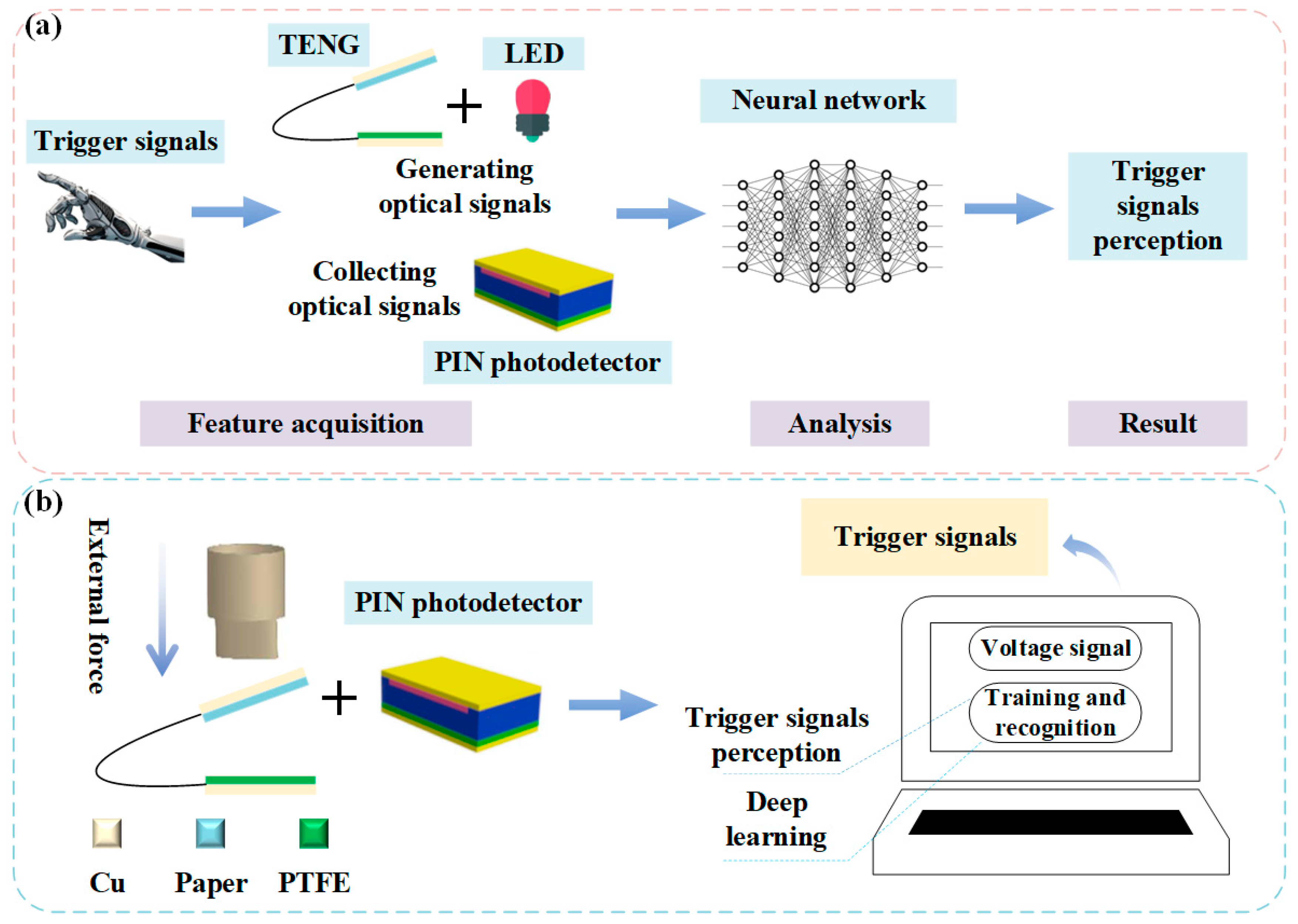
Figure 1. (a) Schematic diagram of trigger signal detection process. (b) Diagram of the trigger signal detection system.
Electronicmat 06 00022 g001
Figure 2. (a) Fabrication Process of Silicon PIN Detector. (b) Images of Silicon PIN Detector. (c) I/V Characteristics of Silicon PIN Detector.
Electronicmat 06 00022 g002
Figure 3. Theoretical performance of the fabricated large-area silicon PIN photodetector. The spectral responsivity (R) and specific detectivity (D∗) were calculated based on the measured dark current of 99 nA at a reverse bias of 30 V, assuming a quantum efficiency of 0.7. The device exhibits a peak responsivity of 0.54 A/W and a high detectivity of 1.05 × 10¹² Jones at 972 nm, verifying its high sensitivity for optical sensing applications.
Electronicmat 06 00022 g003
Figure 4. (a) Fabrication Process of TENG. (b) Principle of TENG. (c) COMSOL simulation potential diagram: (i) d = 1 mm, (ii) d = 2 mm, (iii) d = 3 mm (top layer is Paper and bottom layer is PTFE; d is the distance between the two layers).
Electronicmat 06 00022 g004
Figure 5. (a) Output Voltage of TENG. (b) Output Current of TENG. (c) Load power of TENG. (d) Load Current of TENG.
Electronicmat 06 00022 g005
Figure 6. Schematic diagram of human trigger signals recognition.
Electronicmat 06 00022 g006
Figure 7. Schematic diagram of the self-powered sensing system.
Electronicmat 06 00022 g007
Figure 8. CNN-LSTM fusion model network architecture.
Electronicmat 06 00022 g008
Figure 9. Schematic diagram of data collection process. (The blue lines represent the electrical connections of the external biasing circuit.).
Electronicmat 06 00022 g009
Figure 10. Comparison of the raw electrical signal generated by the TENG (blue, left axis) and the demodulated optical signal received by the PIN detector (red, right axis). The optical signal represents the rectified envelope of the electrical signal, demonstrating that the optical communication channel effectively filters out high-frequency electrical noise while preserving the key morphological features required for pattern recognition.
Electronicmat 06 00022 g010
Figure 11. CNN-LSTM network accuracy and loss function: (a) CNN-LSTM network accuracy; (b) CNN-LSTM network loss function.
Electronicmat 06 00022 g011
Figure 12. Benchmarking analysis of different classification algorithms on the robustness test dataset. The dataset incorporates random temporal shifts and noise interference to simulate complex operating conditions. The proposed CNN-LSTM architecture achieves the highest accuracy of 98.6%, significantly outperforming traditional SVM (68.0%), standalone CNN (78.2%), and standard LSTM (89.4%) models, demonstrating its superior capability in extracting spatiotemporal features from TENG signals.
Electronicmat 06 00022 g012
Table 1. Hyperparameter settings of CNN-LSTM network.
LayersTypesParameters
1Input-
2Sequence Folding Layer-
3Convolution Layer 164 2 × 1 convolutions with stride [1 × 1]
4Batch Normalization 1-
5ReLU-
6Max-pool 12 × 1 pooling kernel with stride [2 × 1]
7Convolution Layer 232 2 × 1 convolutions with stride [1 × 1]
8Batch Normalization 2-
9ReLU-
10Max-pool 22 × 1 pooling kernel with stride [2 × 1]
11Sequence Unfolding Layer-
12Flatten Layer-
13LSTM Layer 1LSTM with 32 hidden units
14Dropout25% dropout
15Fully Connected-
16Softmax-
17Classification-
Table 2. Model evaluation results.
ModelsPrecision (%)Recall (%)F1-Score (%)Accuracy (%)
CNN88.0188.6988.1287.94
LSTM87.5388.2487.6487.64
CNN-LSTM92.9293.3593.1192.94
Table 3. Trigger signal category classification results.
ModelsTypesPrecision (%)Recall (%)F1-Score (%)
CNNM97.9696.3997.17
E69.718476.19
W86.4477.2781.60
R97.9197.1097.50
LSTMM97.3794.4795.90
E68.9483.9475.70
W85.7176.8381.03
R98.1097.7397.91
CNN-LSTMM95.1895.5695.37
E86.4690.8388.59
W92.1687.8589.95
R97.8899.1498.51
Table 4. Performance comparison between this work and other self-powered sensing systems.
Ref.System TypeData TransmissionProcessing MethodAnti-EMI CapabilityTarget Recognition
[40]TENG + PINDirect CircuitCircuit Model AnalysisLowLight Intensity
[44]Flexible TENGElectrical (Wired)Signal Statistics/FilteringLowMotion States
[36]Wireless SpirometerRF WirelessGUI/Pattern MatchingLow (RF Interference)Breathing Pattern
This WorkCS-TENG + PINOptical WirelessCNN-LSTM NetworkHigh (Optical Isolation)Human Action Triggers
Disclaimer/Publisher’s Note: The statements, opinions and data contained in all publications are solely those of the individual author(s) and contributor(s) and not of MDPI and/or the editor(s). MDPI and/or the editor(s) disclaim responsibility for any injury to people or property resulting from any ideas, methods, instructions or products referred to in the content.