Abstract
In this article, thermal investigation methods for electrically insulating and thermally conductive substrate materials will be presented. The investigations were performed in their real-world application environment, i.e., in the form of IGBT (insulated gate bipolar transistor) module substrate plates. First, the overall thermal resistance and thermal structure function of the system in a multivariable parameter space were revealed using CFD (computational fluid dynamics) simulations. Afterwards, thermal transient testing was performed on real samples, with the help of which the thermal resistance values of the modules were determined using the thermal dual interface test method. The presented tests are not intended to determine material parameters, but to rank different substrate materials based on their thermal performance.
1. Introduction
In recent decades, green energy, environmental awareness and sustainability have been increasingly emphasized in both research and development. Electricity is perhaps the closest way to a sustainable economy, in which a key role is played by improving manufacturing technologies, efficiency, reliability and expected useful lifetime of the elements and components utilized in different applications. With such goals in mind, the PowerizeD Project [1] consortium involves 61 companies from 13 countries in cooperation; it was launched by the European Union and the Chips JU (Chips Joint Undertaking [2]) partnership. The primary objectives of the project are greater efficiency and greener operation [3,4,5], the development and investigation of novel materials [6,7,8,9], increased reliability [10,11,12,13], robust and secure operation [14], functional integration [15] and effective collaboration without revealing sensitive data [16,17]. The project places a strong emphasis on lifecycle digital twinning, which includes measurement and extensive reliability testing of the components, as well as modeling and simulation procedures for operation and failure modes, along with estimation of the remaining useful lifetime [18,19,20,21,22,23,24,25,26]. In addition to all this, efforts are also being made to determine and model the ecological footprint of the production and operation of individual components and power units [27,28,29].
As one of the main building blocks of power electronic devices, Insulated Gate Bipolar Transistors (IGBTs) are one of the main focuses of the PowerizeD project. IGBTs are three-terminal, four-layer (pnpn/npnp) power semiconductor devices that combine the advantages of Metal-Oxide-Semiconductor Field Effect Transistors (MOSFETs) and Bipolar Junction Transistors (BJTs). That is, they provide almost power-free control by means of an electric field, have excellent conductivity and can withstand high reverse bias. In terms of switching speed, they are somewhere between power BJTs and FET devices.
IGBTs are typically used for fast switching of extremely high powers, typically in the order of hundreds of amperes and thousands of volts. In such conditions, electrical insulation, heat loss removal and cooling of the active layer are equally essential, for which the device carrier plate, i.e., the substrate, is primarily responsible. The thermal resistance of the substrates indirectly affects the module’s capabilities in terms of utilization. A module with a lower thermal resistance between the die and the heat sink surface can operate at a higher power density for the same temperature rise or at a lower temperature for a fixed power density [30].
In power semiconductor devices, Direct Bonded Copper (DBC) is most often used for this purpose, consisting of copper layers directly bonded to one or both sides of a ceramic substrate. The ceramic substrate material can be, for example, Alumina (Al2O3), Aluminum-Nitride (AlN), or Silicon-Nitride (Si3N4). The latter two ceramics have better thermal conductivity, but their manufacturing cost is significantly higher.
Another solution to ensure electrical insulation and good cooling of IGBT modules is the so-called Insulated Metal Substrate (IMS) [31]. The IMS consists of a metal substrate, an insulating layer with high thermal conductivity, a plastic frame and a plurality of conductive metal pads. The structure is based on the metal substrate or metal core, which is coated on its entire top surface with an insulating layer. The plastic frame with the apertures for the metal conductive pads is placed on the top of the insulating layer coating the metal core.
The thermal performance of the ceramics used in DBC substrates is typically better than that of the polymer-based dielectric layers used in typical IMS substrates [32]. However, while the mechanical strength of ceramic insulating plates and the difference in thermal expansion coefficients result in certain design constraints, the polymer insulation of IMS substrates allows for much more flexible solutions. The thickness of the insulating layer can be freely designed and even multilayer solutions can be created. The manufacturing costs of IMS carriers are also typically lower.
A number of studies deal with the comparative examination of DBC and IMS carriers. In paper [32], the two carrier types were specifically compared from a thermal perspective. First, steady-state and transient analyses were performed using the COMSOL MULTIPHYSICS finite element simulation tool, examining the theoretical junction temperatures and thermal impedance curves. The study was then supplemented with further experimental investigations, where SiC MOSFETs in a half-bridge configuration were tested under high power. Thermal measurements were performed using a thermal camera and precalibrated thermocouples. IMS carriers showed similar thermal performance in steady-state to DBC, thanks to the large heat-spreading metal layer under the chips, and could even outperform it during a low-frequency switching operation due to the high thermal capacity.
Another study [33] compares a Double-Sided Cooled (DSC) Al2O3-based DBC and a highly thermally conductive Epoxy Resin Composite Dielectric (ERCD) substrate using finite element modeling. As a result, the equivalent junction-to-case thermal resistance of the organic-based ERCD substrate outperforms that of the Al2O3 DBC by about 10%, while its manufacturing cost is only about 1/3 of that.
The effect of thermo-mechanical stress on different types of substrates can be investigated using power cycling [34]. In the first step of the study, the cycles to failure were determined using finite element modeling and the Darveaux model for a reference DBC and four different IMS arrangements. As a second step, physical samples of the arrangements used in the simulation were also tested. The experiment was carried out until the complete failure of the samples (open- or short-circuiting) and was supplemented using a Scanning Acoustic Microscope (SAM). The absolute number of cycles to failure is not indicated in the article, but the simulations show a deviation of approximately −40…+60% compared to the experimental results. The minimum cycles-to-failure values are similar to those of DBC in only one IMS type; in the other three cases, the IMS arrangement significantly underperforms. Thermal measurements results achieved during the experiment are not presented in the article if there are any.
Substrates carrying power semiconductors, and thus IGBTs, are the subject of continuous development and research in order to enhance thermal conductivity and reliability along with possibly reducing manufacturing costs (e.g., [35,36]).
The development of four new, novel IMS materials was also an important objective within the framework of the PowerizeD project. The basic criterion for the new materials was at least the same or better thermal conductivity. This was tested in two ways: on the one hand, using material testing methods at other project partners, and on the other hand, using real test vehicles, i.e., by testing IGBT devices mounted on IMS substrates made using all four of the new materials.
At the Budapest University of Technology and Economics, we performed thermal testing of the device-level IGBT modules using both simulations and measurements. First, preliminary simulations were performed on thermal test vehicle models in order to determine the optimal chip size for subsequent thermal transient testing measurements [37]. After that, the necessary preliminary investigations were carried out on the pilot samples received from the project partners, and then the new IMS materials were tested by comparing the measurement results of a higher number of samples with the thermal performance of the conventional DBC substrates.
2. Measurement Methodology
2.1. Thermal Transient Testing of Packaged Semiconductor Devices
The popularity of thermal transient testing is due to its wide applicability. It allows us to test semiconductor packages and modules, identify fault locations and structural design elements and perform thermal qualification. It is also a powerful measurement tool to verify and refine thermal simulations. This non-destructive characterization technique allows for a single electrical measurement and subsequent automated software evaluation to “see” the internal structure of an electronic component. The internal thermal resistances and thermal capacitances can be revealed at all levels of the structure, starting from the active layer of the chip, reaching throughout the heat dissipation path of the whole package to the environment via the electronics carrier board, heatsink and device housing. Furthermore, this method can even provide reliable temperature data on internal structural elements in the thermal path that are otherwise inaccessible [38].
During thermal transient testing, a sudden power change is created on the device under testing. The goal is to record the thermal transient from the moment of switching on, which can be done by measuring a selected temperature-sensitive parameter, usually a forward voltage over a pn-junction. Dividing the transient of the temperature-sensitive parameter by the dissipation step value, one can obtain the so-called Zth function. In addition to the Zth function, there are other representations for expressing thermal impedance, such as the so-called integral or differential structure functions. These can be obtained using the NID method (Network Identification by Deconvolution), which is associated with the name of Professor Vladimír Székely [39].
The structure function describes the cumulative heat capacity of the main heat conduction path, considered as one-dimensional, as a function of the cumulative thermal resistance. The starting point of the structure function corresponds to the heat source, i.e., the dissipating region (e.g., a pn-junction), while the environment with infinite heat capacity always causes a singularity that goes to infinity. Any change in the main heat conduction path between the measurements creates a so-called separation point in the structure functions, i.e., the starting point of the separation of the curves. Such changes may occur, for example, due to degradation of the encapsulation, delamination of structural layers, or the formation of voids, but such deviations can also be intentionally created to define certain section boundaries of the heat conduction path. The latter is a well-established and standardized laboratory procedure called the Transient Dual Interface Test Method (TDIM) for determining the package boundaries of semiconductor devices during thermal characterization [40].
2.2. Thermal Transient Testing of Single pn-Junctions
Thermal transient measurements of semiconductor devices are most often performed on diodes or two-terminal devices. This is due to the fact that many measurement procedures also use simplifications for three or more-terminal devices that can be reduced to a simpler two-terminal measurement.
Modern characterization instruments are often equipped with more complex power supply options, offering the user a variety of voltage and current sources for different measurement arrangements, but these are not necessarily available at high power levels. In such cases, two-pole methods are also typical.
Four-wired Kelvin measurement arrangements are always necessary, i.e., two current sources and two data acquisition channels are connected to the diode terminals. The power step is achieved by switching a heating current on and off while maintaining a constant measuring current across the device, allowing the measurement of the temperature-sensitive forward voltage during the cooling transient of the device.
2.3. Measuring the Cooling Transient
Cooling transient measurement is the most commonly used type of thermal transient testing, where the device is first supplied with the so-called heating current until it reaches a thermally stable state, and then the power jump is created by switching off to the measuring current. From the moment of switching off, the so-called cooling curve, the change in the temperature-sensitive parameter, i.e., in this case, the forward voltage, is recorded.
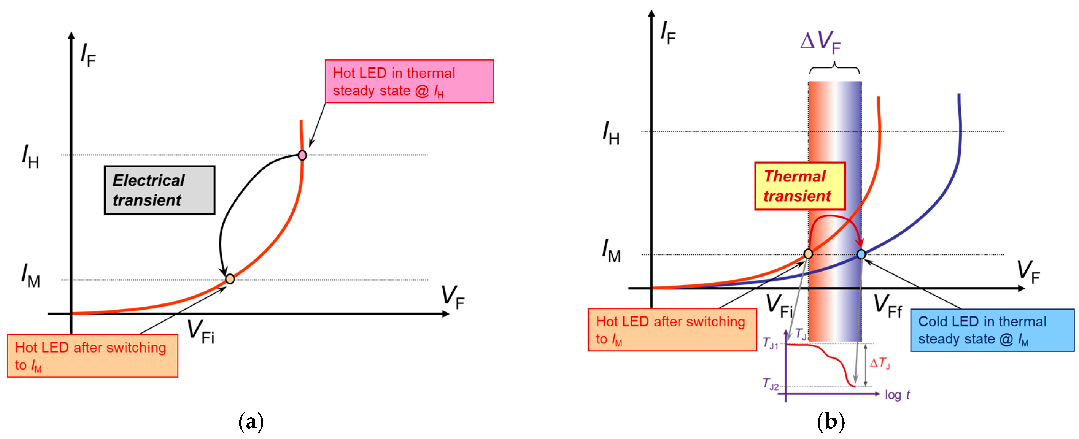
After the switch-off, an electrical switching transient occurs first, typically in the range of several hundred mV and 10–100 μs (Figure 1a). After that, the transient of purely thermal origin is recorded (Figure 1b). During this time, the forward voltage captured by the measuring current increases continuously from the initial hot operating condition until the thermally stable cold state of the device.

Figure 1.
(a) Electrical transient on the output characteristic of a diode during switching from heating current to measuring current. (b) Thermal (cooling) transient on the diode output characteristic at the measuring current. (Reworked figures after reference [41]).
2.4. Thermal Transient Testing of Three-Pole Devices
Three-terminal devices typically have a discrete, single active component inside the package. The three poles offer a variety of powering and sensing options. Multiple connections can be used for powering, while one single pair can be used to measure the temperature-sensitive parameter. By connecting two terminals together, the measurement procedure can typically be simplified, thus reducing it to the two-terminal measurement procedure (i.e., measuring simple pn-junctions) previously described.
In the case of a current step, the power jump in discrete semiconductor devices can be calculated by the change in the current fed into the device and the temperature-dependent parameter, most often the current- and temperature-dependent change in the forward voltage. This measurement method has several advantages. For example, it allows the highest power jump to be achieved on three-terminal devices without the use of special fast high-voltage switches. Furthermore, the measurement current can be chosen to be sufficiently low, thus simplifying the calibration of the devices [38].
However, the charging and discharging of the diffusion capacitance of, e.g., an emitter–base pn-junction can be slow, resulting in a long electrical transient. Furthermore, the power is limited by the forward voltage due to the supplied current, similar to the case of diode measurements.
2.5. Creating a Power Step by Changing the Voltage
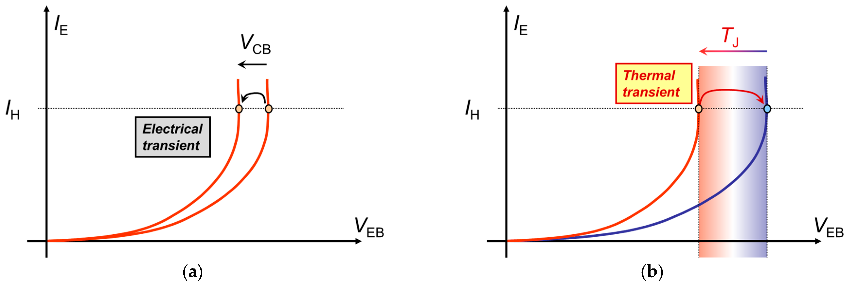
In the case of a voltage step, a continuous emitter current is maintained on the device, and the power jump is generated by switching the collector–base voltage between high and low values. The temperature-sensitive parameter is still the emitter–base voltage. In this arrangement, the powering and the sensing branches are separated.
This measurement method takes place with a shorter electrical transient, since the largest source of the electrical transient is in most cases the diffusion capacitance, which is almost constant with a constant emitter current. For this reason, the measurement is also suitable for mapping finer thermal structures.
During the measurement, the higher collector–base voltage, i.e., the heating power, is switched to a lower value. As a result, the emitter–base voltage decreases (i.e., the electrical transient, Figure 2a). After the electrical transient, the emitter–base voltage starts to increase as a function of the temperature change (i.e., the thermal transient, Figure 2b).
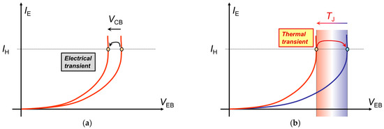
Figure 2.
(a) Electrical transient on the output characteristic of a diode during turn-off from a higher collector–base voltage to a lower one. (b) Thermal (cooling) transient on the diode output characteristic at the smaller collector–base voltage. (Reworked figures after reference [41]).
2.6. Thermal Transient Testing of IGBTs
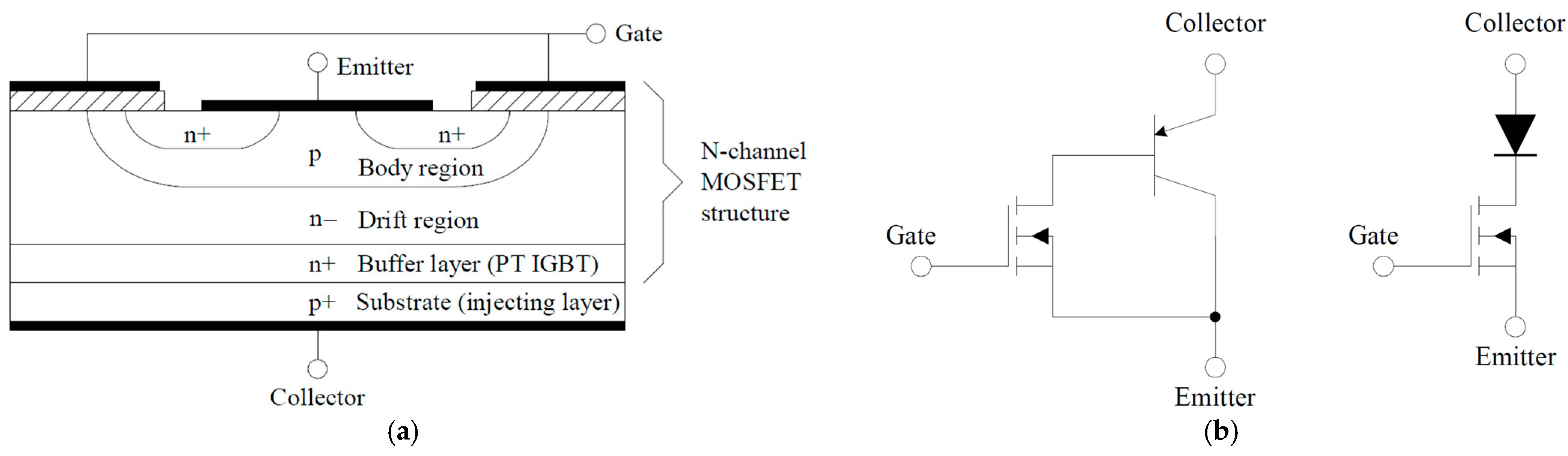
IGBTs are essentially pseudo-Darlington-coupled hybrids of an n-type enhancement MOSFET and a PNP BJT [42]. In the name, “Insulated Gate” refers to the MOSFET-like, high-impedance input, while the designation “Bipolar Transistor” refers to the output BJT, also referring to the fact that both types of charge carriers participate in the current conduction. Figure 3a illustrates a basic four-layer planar structure.
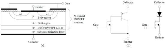
Figure 3.
(a) Structure and (b) simplified equivalent circuits of an N-channel Insulated Gate Bipolar Transistor [43].
In terms of operation and very simply, if a voltage higher than the threshold value is applied to the Gate electrode, a so-called inversion channel is formed in the p Body region directly below the Gate electrode due to the attracted electrons. Then the n+ layer of the Emitter can connect to the n- Drift region through the inversion channel, i.e., electrons can enter the Drift region from the Emitter. If the Collector is positively biased relative to the Emitter, the pn-junction between the p+ Substrate layer of the Collector and the n- Drift layer is forward-biased, i.e., the pn-junction located here will conduct.
Both the cross-sectional diagram and the circuit equivalent diagram (see in Figure 3b) clearly show the PNP BJT, which is formed by the p Body region, the n- Drift region, and the p+ Substrate; in the arrangement, during normal operation, the base–emitter junction of the PNP BJT is reverse-biased.
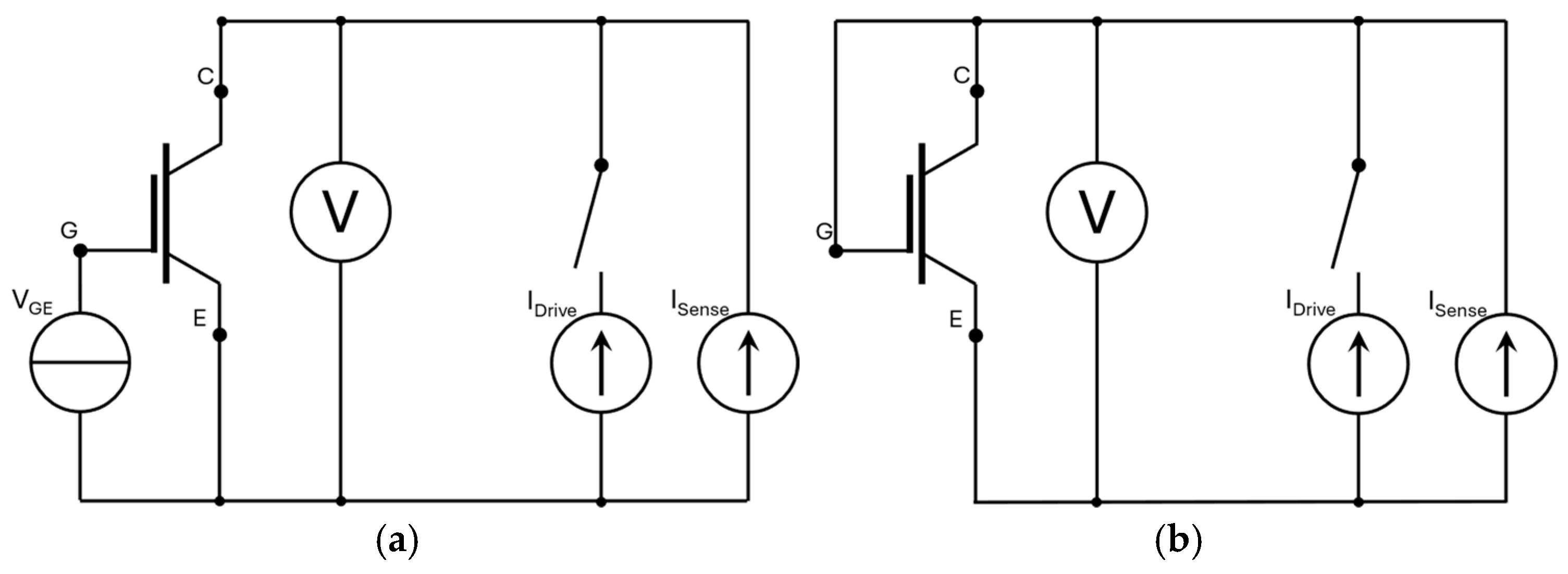
The characteristics of IGBTs are similar to those of MOSFETs but shifted to the right by the voltage of the internal pn-junction (i.e., the junction of the p+ Substrate and the n- Drift region). At high gate voltages, the channel resistance will be very low, and the device characteristics will be dominated by the series pn-junction. Therefore, the measurement becomes similar to the setup for diode measurements described in the previous sections. For testing IGBTs, the measurement method shown in Figure 4a is applied most of the time [44]. However, the gate and collector terminals may be shorted as a simplification of the setup, thus achieving a diode-like operation during thermal transient testing (Figure 4b). In case of MOSFETs for example, a popular measurement procedure is to convert the device into a so-called “MOS diode” by shorting the gate and the drain terminals [45].

Figure 4.
(a) Schematic of the typical IGBT thermal transient testing setup. (b) Schematic of the diode-connected IGBT thermal transient testing setup.
2.7. Transient Dual Interface Test Method
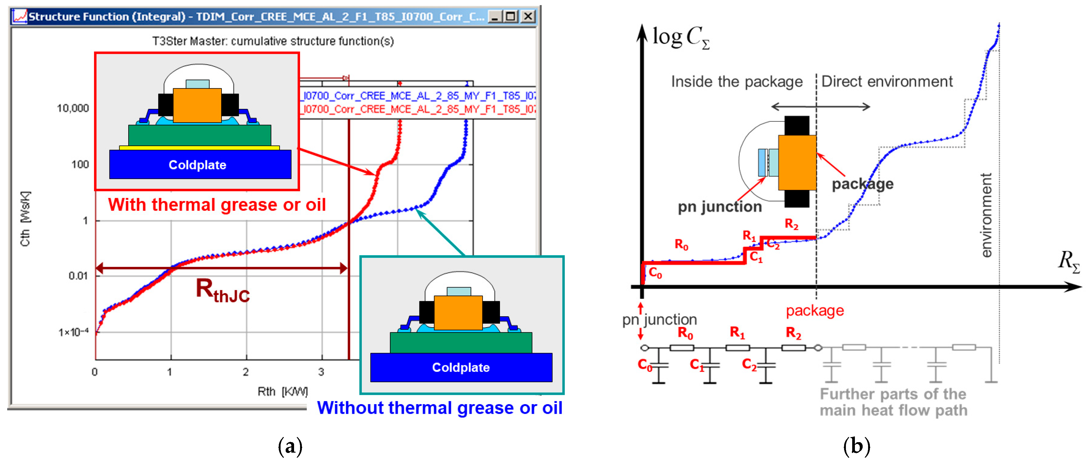
The Transient Dual Interface Test Method is described in the JEDEC JESD51-14 standard [40], describing the measurement of devices with accessible heat sinks. The procedure relies on an intentionally created change in the devices’ structure functions, performing the previously discussed thermal transient testing method via two different thermal interfaces. These thermal interfaces are applied between the external cooling surface of the device and a temperature-controlled cold plate, therefore revealing the so-called junction-to-case thermal resistance (RthJC) of the packages. The standard specifies a dry (air gap) and a wet (e.g., thermal paste or thermal oil) boundary condition. In practice, however, it is possible to deviate from what is strictly prescribed in the standard, and it is often even advisable to do so: for example, applying two different dry thermal boundaries, or contrarily, two different wet conditions instead. Figure 5 briefly illustrates the essence of the procedure.

Figure 5.
(a) Integral structure functions with and without thermal grease or oil [40]. (b) Determining the thermal model of a power LED package based on thermal transient measurements performed according to the JESD51-14 standard. (Reworked figures after reference [41]).
3. Simulation Setup, Results and Evaluation
During the parametrization of the thermal test vehicles, two different numerical simulation tools were utilized, which was also advantageous for cross-verification purposes. It is important to note that the preliminary simulations were performed based on theoretical geometric and material parameters only, and it was not possible to calibrate them using real measurement results.
3.1. Simcenter Flotherm
One of the tools was a commercially available software Simcenter Flotherm 2304, created especially for electronics cooling simulation by Siemens [46]. As a tool designed specifically for the industry, this software provides many features, like automated meshing (which can be refined manually), thermal(-electric) models for different electronic devices, printed circuit boards, etc., together with parametric sweeping and transient simulation fine-tuned for thermal transient testing and structure function evaluation. The solver itself uses the finite volume method (FVM) commonly utilized for Computational Fluid Dynamics (CFD) simulations. The model generated in Flotherm can be seen in Figure 6a.
Figure 6.
CAD model of the IGBT thermal test vehicle as represented in (a) Simcenter Flotherm and (b) in SUNRED simulator environments.
3.2. The SUNRED Simulator
SUNRED is our in-house simulator for Finite Volume Modeling and efficient computation of thermal and electrothermal problems of solid structures [47]. The simulator is named after the SUccessive Network REDuction algorithm that computes the equations of the Finite Volume Model (FVM). The algorithm converts the FVM equations into an electrical network model and computes the solution of this circuit. It has an advantage over commercial simulators in that it directly supports several specific problems in microelectronics (calculating the light emission of LEDs and OLEDs, light conversion in the phosphor layer of LEDs, handling the hysteresis of vanadium dioxide, etc.). The latest version is HexMG, in which the subcircuits can be freely specified with a netlist so that the simulator does not require modification of the solver kernel for problems not previously supported; only the extension of the framework is necessary [48].
Figure 6b represents the model generated in the SUNRED environment.
3.3. Steady State Analysis
The aim of static thermal analysis was to determine the overall thermal resistance and temperature rise at specific power values.
The simulation conditions were 20 W volumetric static dissipation in the chip and thermal ground beneath the boards, while convective heat transfer was omitted from the simulations.
The simulations were performed for both the conventional Direct Bonded Copper layout and the Insulated Metal Substrate case. In case of the IMS boards, the project worked with geometric dimensions and theoretical material parameters received from partners (which are project confidential data and therefore cannot be published for the time being).
First, the variation in thermal resistance as a function of chip size was investigated. The conductivity of the system Thermal Interface Material (TIM) was chosen to be 3 and 10 W/m·K, respectively, with a presumed constant 100 µm thickness value. For the variation in chip edge sizes, 1, 2.5, 5 and 10 mm lengths were examined. The results of the simulation series are shown in Figure 7a.
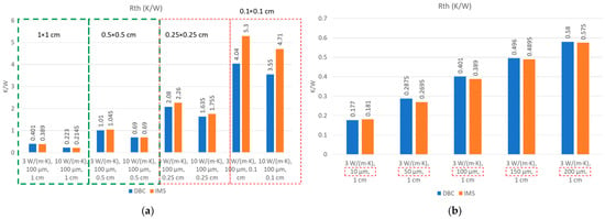
Figure 7.
Variation in the overall Rth thermal resistance as a function of (a) chip edge size and (b) system TIM thickness.
In the next round, the effect of varying the thickness of the system TIM on the overall thermal resistance value was examined. During this, a TIM material with a thermal conductivity of 3 W/m·K and a chip with a fixed side length of 10 mm were assumed. Figure 7b shows the simulation results for 10, 50, 100, 150 and 200 µm system TIM thicknesses.
3.4. Thermal Transient Analysis
The purpose of this study was to assess the impact of die attach quality on overall measurement.
A theoretical 20 W stepwise excitation was generated on the chip. DBC and IMS were both investigated again, with the geometry and material parameters achieved from the project partner. Both Flotherm and SUNRED simulation environments were used again. With regard to the previously changing parameters, a complete parameter sweep was performed in this study. Thermal conductivity of the system Thermal Interface Material was set to be 3, 4, 5, 10 W/m·K with a varying thickness of 10, 50, 100, 150 and 200 µm. The length of the square chip edge was set to be 1, 2, 2.5, 5 and 10 mm, respectively.
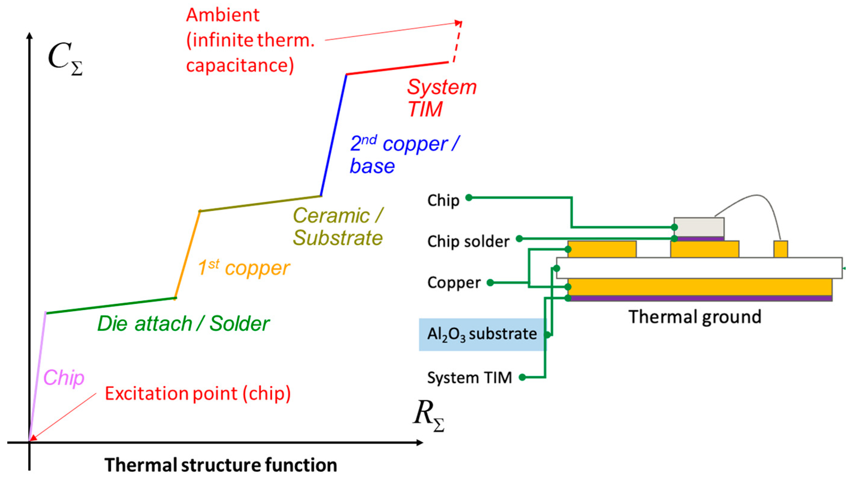
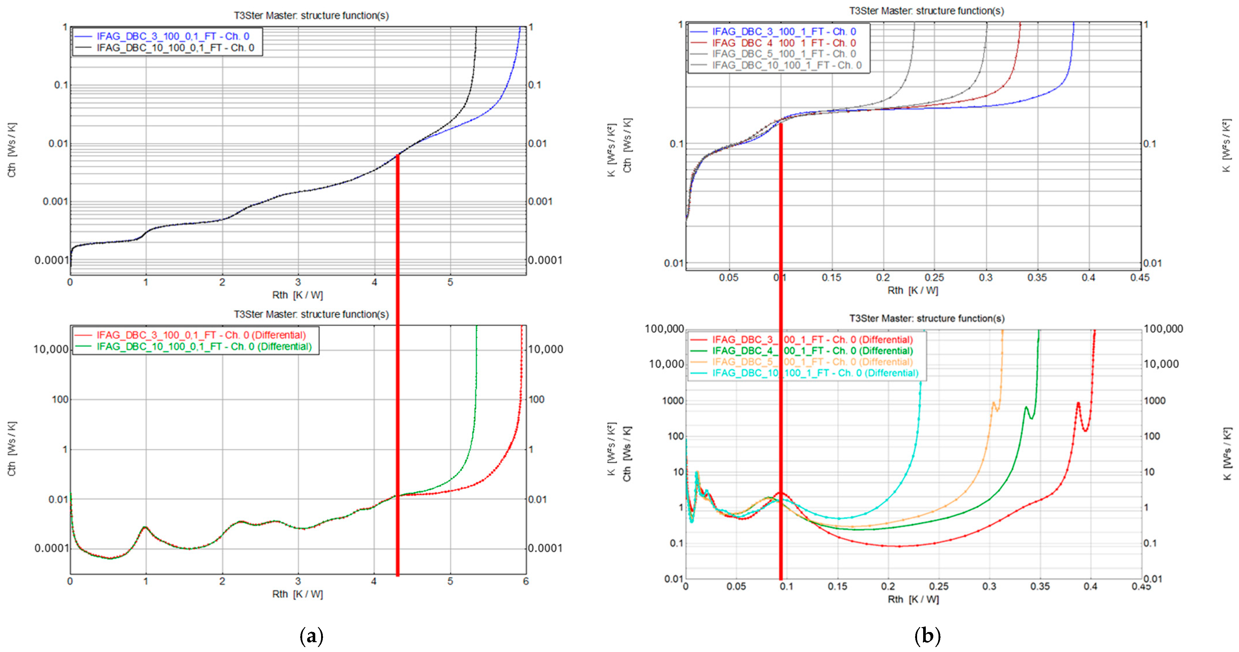
Figure 8 shows a theoretical interpretation of the integral structure functions obtained as a result of the simulations. Figure 9a,b represent the obtained integral and differential structure functions in case of chip edge lengths of 1 mm and 10 mm.
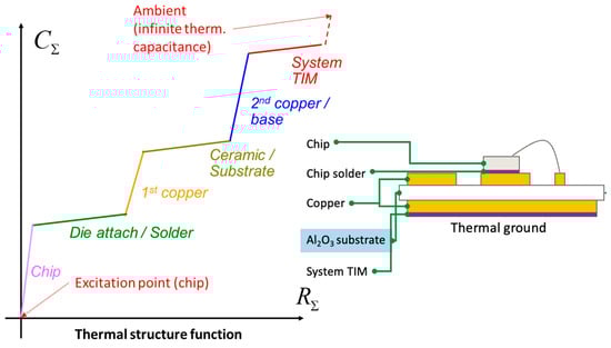
Figure 8.
Theoretical interpretation of the integral structure function of a Direct Bonded Copper carrier board, distinguishing the individual structural layers on the curve.
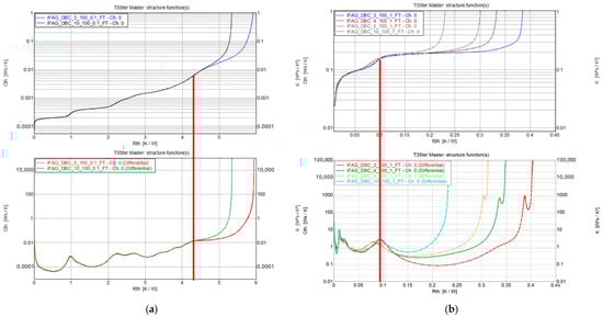
Figure 9.
Integral (top) and differential (bottom) structure functions obtained for chip edge sizes of (a) 1 mm and (b) 10 mm. The separation points caused by the system TIMs of different conductivity are marked by vertical red lines.
3.5. Evaluation of the Simulation Results
In light of the simulation results, we can somehow formulate different requirements for optimizing the test samples for thermal transient testing by real measurements.
The pure geometrical and material properties of the DBC and IMS boards suggest negligible differences between the overall net resistances, the assumption of which is in contradiction to the simulation results (Figure 7a). The possible reason for this may be that in the case of BDC and IMS, the cone of the main heat-flow path in the structure changes significantly under small-area chips, which makes it impossible to appropriately rank the thermal performance of the substrate materials by comparing thermal transient testing results of physical samples. For this reason, based on the simulation results, it is a basic requirement that the chip size should be larger than 2.5 mm × 2.5 mm.
In contrast, in the case of larger chip sizes, the overall thermal resistance value will be very small (Figure 7a), which in itself represents a serious measurement challenge in the field of thermal transient testing. In addition, the effect of the system TIM thickness variation is comparable to the total thermal resistance value for chips with 5 and especially 10 mm edge lengths (Figure 7b).
Also, for bigger chip sizes (e.g., 5 or 10 mm edge lengths), the cone of the main heat-flow path will also be wider in area. This means the IGBT substrate can spread the heat conduction to an even larger area, resulting in a smaller thermal resistance until the bottom surface of the substrate. For this reason, the overall thermal resistance will increasingly be determined by the quality of the system TIM with relatively poor thermal conductivity. At the same time, the structure of the DBC and IMS appears in the structure functions to an ever-smaller extent and with a decreasing resolution, as can be clearly noticed in Figure 9a,b.
Figure 9b draws attention to another important phenomenon. As the chip surface area increases, the thermal conductivity of the system TIM has an increasing effect on the heat conduction in the substrate. In the case of a TIM with good thermal conductivity, the cone of the main heat flow path in the substrate is smaller, which is why the structural layer corresponding to a given cumulative thermal resistance will also appear with a smaller heat capacity in the structure function. By contrast, in the case of a TIM with poorer thermal conductivity, the heat conduction in the substrate is distributed over an increasingly larger surface, which is why this layer has a relatively smaller cumulative thermal resistance and a larger cumulative heat capacity. The result of all this is that the slope of the section of the structure function corresponding to the substrate changes due to the variation in the TIM thermal conductivity. This feedback effect definitely degrades the accuracy of the thermal dual interface testing method, as it makes the separation point reading much more uncertain.
Based on the evaluation of the simulation results, the 5mm chip edge length may seem to be a suitable compromise for the preparation of later measurement samples for the in situ qualification of the thermal performance of the substrate material through thermal transient testing.
4. Measurement Setup, Results and Evaluation
4.1. Test Samples and Preliminary Tests
In order to investigate the thermal properties of the new types of substrates by in situ physical measurements as well, 10 mm × 10 mm chips were mounted onto test boards. A total of 4 × 10 samples were made from the four different types of new IMS substrates (Insulated Metal Substrate), and 10 + 10 pieces were created from DBC (Direct Bonded Copper) samples to serve as a reference.
The total of 60 samples required multiple time-consuming measurements. In preparation for the mass measurements, the first 10 BDC panels were utilized to develop an appropriate workaround for the correct implementation of TDIM tests. During this, the calibration of the Temperature-Sensitive Parameter (TSP—here, the gate–emitter voltage VGE) was performed for all the different thermal interfaces using a water-cooled controlled thermostat. To achieve consistent and reliable measurement results, TDIM measurements were tested at several different operating points and at different ambient temperatures. This meant that different power dissipation was characteristic at these different operating point values, and the thickness of the thermal pastes was also different at intentionally varied ambient temperatures. In order to ensure the feasibility of completing the task within the available timeframe, viable options for speeding up the measurements were examined during the preliminary investigations.
To perform thermal transient testing, the power supply and transient measurements were performed using a T3Ster SI instrument from Siemens [49], in a four-wire Kelvin arrangement. For this purpose, a custom measuring assembly was created, the pilot version of which was made from spring-loaded pins mounted on a prototyping PCB. The mechanical fastening was provided by a lever clamping, which allowed for quick and easy replacement of the samples. The contacting pin bed and the clamping mechanism are shown in Figure 10a,b, respectively.
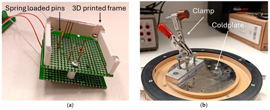
Figure 10.
(a) Contacting pin bed and (b) clamping mechanism of the test fixture. Consistency between measurements could be ensured by always positioning the fixture in the same way. This required greater operator attention, but creating such pilot versions provides the fastest possible solution for designing the final, appropriate test fixture. For the final characterization of the samples, a 3D-printed frame was added to the fixture to ensure consistent spring preload and proper positioning.
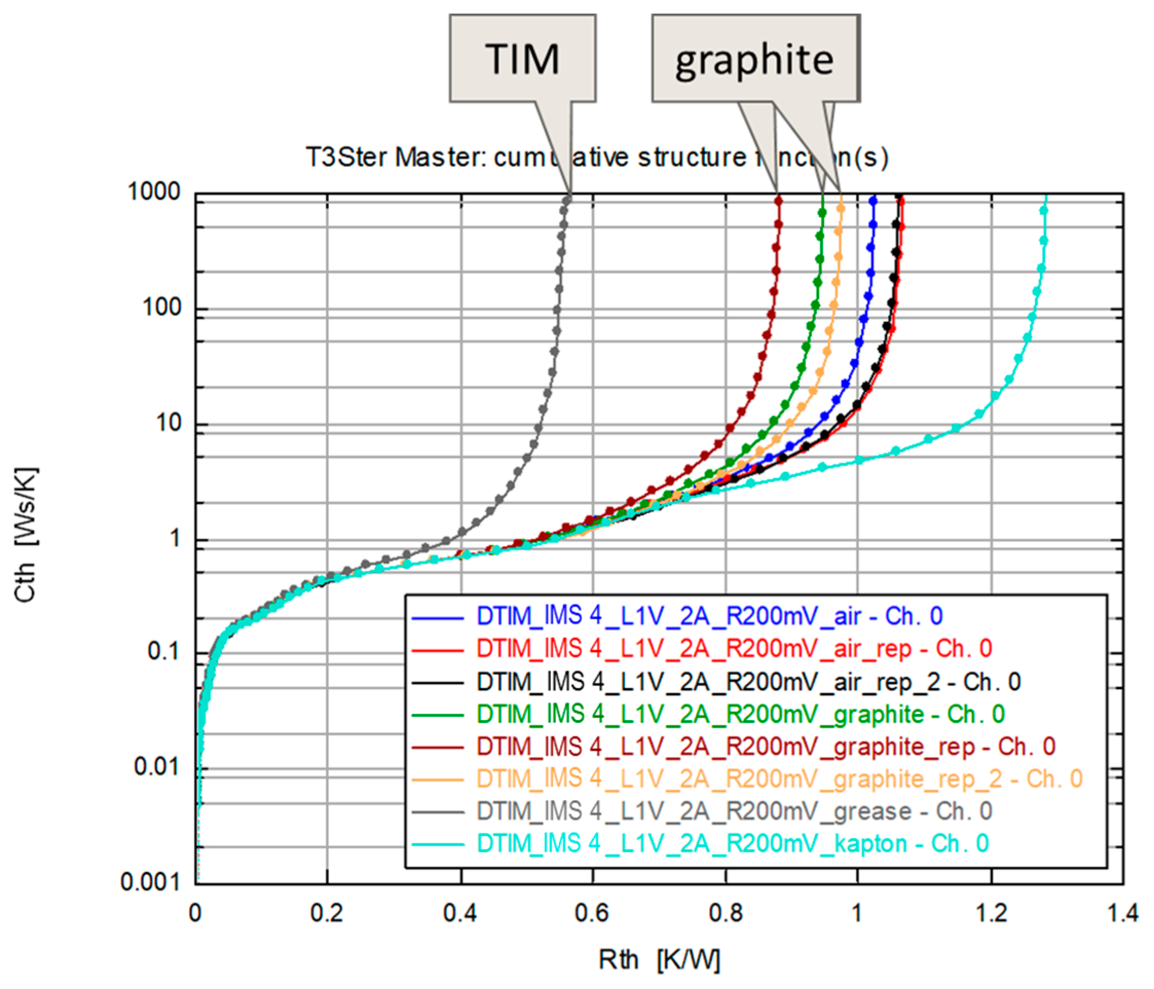
Several different thermal boundary conditions were tested to identify the bottom interfaces of the test boards, such as airgap, a thermal conducting graphite sheet, thermal insulating kapton tape and thermal greases with different thermal conductivities. To examine the repeatability and uncertainty of the measurements, thermal transients belonging to certain boundary conditions were captured several times.
An example of the preliminary test results is illustrated in Figure 11. The structure functions belonging to different thermal boundary conditions are clearly separated, but the separation point itself cannot be determined with great certainty in all cases. While the measurement repeatability is within 10% accuracy, it can be clearly observed in the case of dry boundary conditions that the slopes of the sections representing the changing boundary transition itself (graphite layer, air gap, kapton) differ only very slightly; thus, this part of the structure functions is mostly blurred. For this reason, we decided to use a thermal grease with a higher and a lower thermal conductivity coefficient for the final TDIM tests.
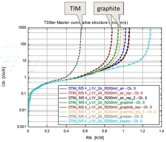
Figure 11.
Structure functions of the same test board determined along different thermal boundary conditions, from the left to the right in order: thermal grease, graphite sheet ×3, air gap ×3, kapton tape.
4.2. The Final TDIM Test Setup
The final measurements were performed with the gate and collector terminals of the IGBTs short-circuited, i.e., measuring in a diode-like two-pole arrangement. The heating and sensor current values were set to be 2 A and 100 mA in order, while the ambient temperature was kept at a constant 25 °C. The power step value achieved in this way was around 13.5 W, which may seem to be quite small for IGBT devices with overall thermal resistance around 0.2 K/W. However, the preliminary measurement results reveal that even with such a small power step, thermal transient curves with a sufficiently good signal-to-noise ratio could be recorded.
The parameters of the measurement setup were otherwise determined to comply with the tested IGBTs, the T3Ster SI used, and the maximum 0.5 °C error limit allowed in the corresponding JEDEC standards, also keeping in mind the fastest possible completion of TDIM tests without compromising measurement accuracy and repeatability.
Based on the pilot fixture, a dedicated, enclosed design test fixture was later created, carrying four panels at once, thus enabling them to be measured simultaneously. At the same time, the entire fixture was moved from the water-circulating thermostat to a much faster, Peltier-based temperature-controlled cold plate, reducing the time required for TSP calibration by about an order of magnitude. The final quad test sample carrier fixture is shown in Figure 12.
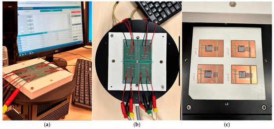
Figure 12.
(a) The Peltier-based temperature-controlled cold plate with the attached enclosed fixture and test samples; in the background, the GUI of the T3Ster SI measurement environment can be seen on the screen. (b) Top view of the test fixture showing the 4-wired Kelvin arrangements. (c) Four samples placed in the 3D-printed positioning frame, guaranteeing consistent sample placement in all cases.
4.3. Results of the TDIM Tests
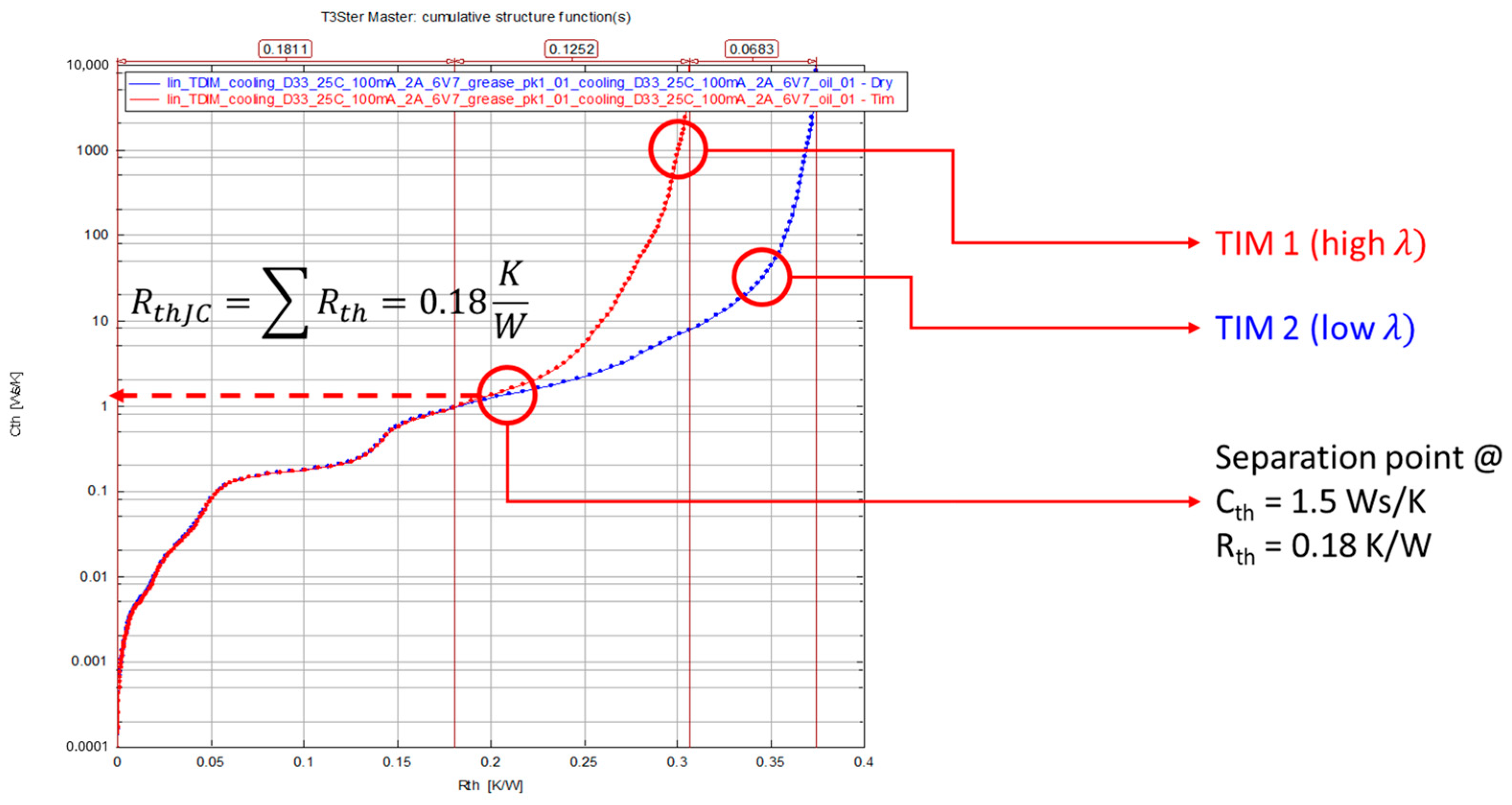
Figure 13 shows an example of the separation that can be obtained by the final measurements. The figure clearly shows that the final results could be extracted from the thermal transient curves with decent certainty. The applicability of the TDIM method, designed and fine-tuned with the help of simulation and preliminary samples, has been proven successfully; prior to the separation point, the curves of the structure functions have a good overlap, while the separation point itself is well defined and can be read from the results even with the automated tool in the evaluation software. Ultimately, the test results show that the separation point was around 0.2 ± 0.05 K/W, which is in good agreement with the simulation results for 10 mm × 10 mm chips.
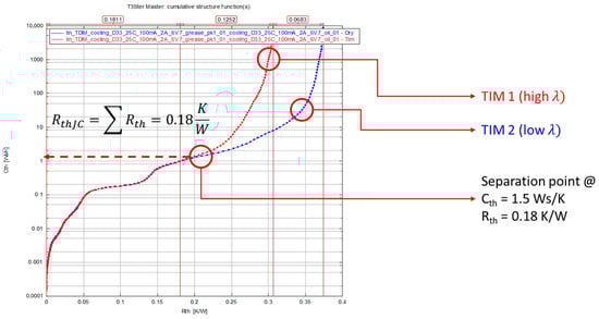
Figure 13.
The final proposed and applied TDIM test method, using one thermal grease with a higher and one with a lower thermal conductivity value. The separation point in this case was determined to be 0.18 K/W, which is the junction-to-case thermal resistance of the test board under testing.
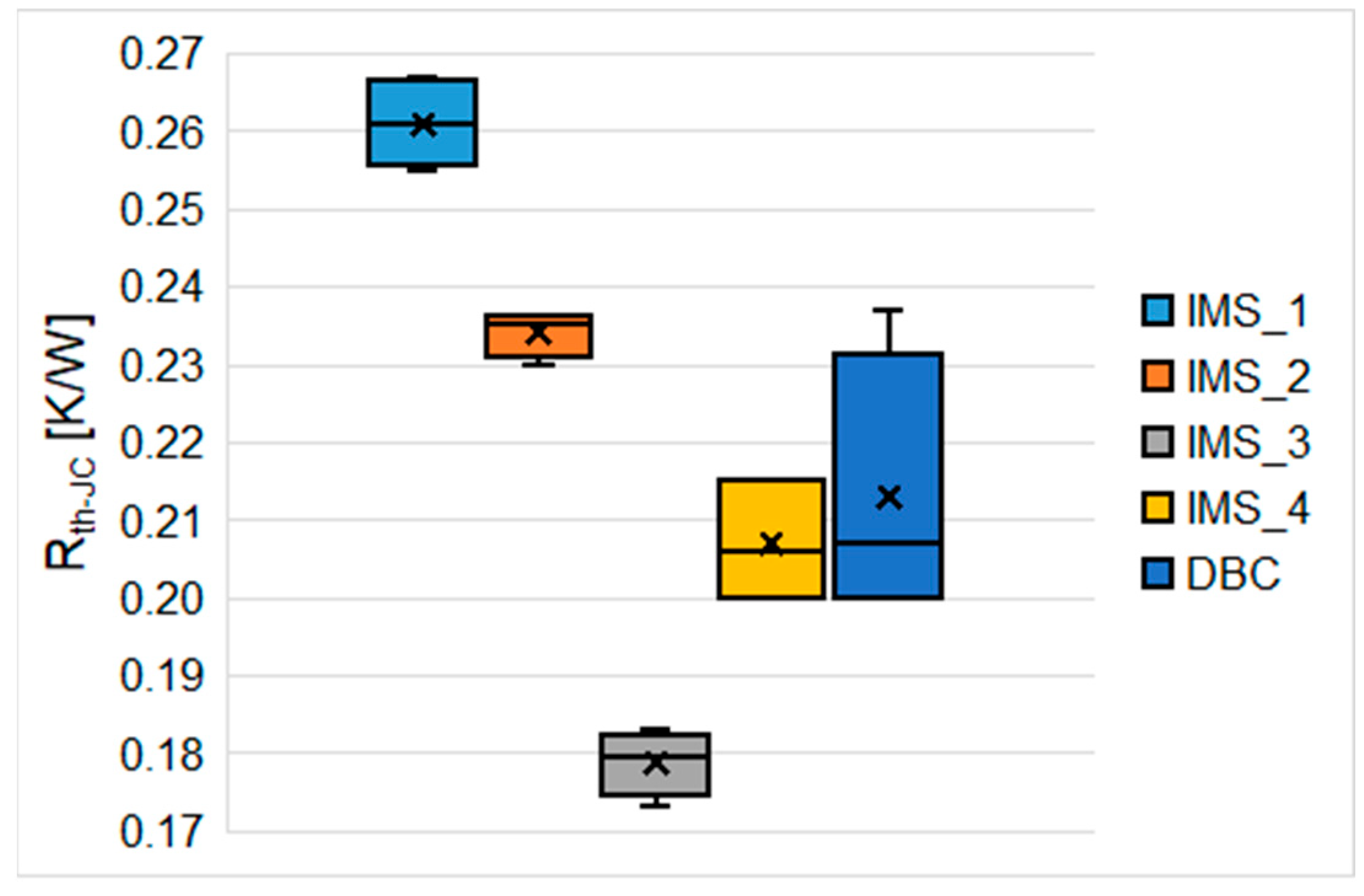
The final results of the tests are illustrated by the box plot shown in Figure 14; the exact results are project confidential and therefore cannot be shown individually. Still, it can be stated that one of the novel carrier materials shows slightly worse performance compared to the baseline DBC arrangement, two are in a similar range and one performs even better.

Figure 14.
Box plot of the junction-to-case thermal resistance values obtained as the final result of the tests. One of the novel carrier materials shows slightly worse performance compared to the previous DBC, two are in a similar range, and one performs even better.
From all of this, we can conclude that the simulation and TDIM measurement setup presented in this article form a successful and efficient investigation method together.
4.4. Discussion on Potential Sources of Experimental Error
To address the experimental limitations, in the case of the thermal investigation discussed in this article, four different potential sources of error could be identified, which are as follows, respectively:
- Uncertainty of thermal transient testing;
- Sample material fabrication differences/tolerances;
- Variations in thermal interface material application;
- Separation point reading uncertainty.
During thermal transient testing performed according to the JEDEC JESD51-1 standard [37], a temperature accuracy of 0.5 °C is typically required. Also, when measuring or setting other metrics, the requirements can also be traced back to the same 0.5 °C accuracy. The temperature transients captured during the investigations were typically in the range of 10 °C, which according to the standard can result in a maximum measurement error of 5%. It is worth noting that thermal experts consider a 10% error margin to be a particularly good value.
The fabrication tolerances of the test samples were not disclosed and are unknown. However, the IGBT chips are from the same wafer; the differences between them are expected to be negligible. Also, a key point of thermal transient testing, the calibration of the temperature-sensitive parameter, was completed individually for each device. In principle, the manufacturing uncertainty of the carrier plates appears directly in the structure functions, but the measurements were prepared to deal with this issue on a high number of samples so that the statistical analysis reduces the effects of such material fabrication variations.
Variations in the application of thermal interface material were also investigated (see in Figure 11), in which case the differences caused were within the range of approximately 10%. However, it is essential to note that the differences caused by the application of TIM appear only after the separation point, i.e., they only affect the structure functions after the separation point. As a result, such errors can only affect the separation point readings; however, if such a small (10–20% value of the total thermal resistance) deviation causes reading uncertainty, it is worth considering replacing the TIMs with ones where the slope difference between the structure functions is much more significant. During the investigations discussed in this article, this analysis was performed and the thermal interfaces were chosen accordingly.
The uncertainty of the separation point reading is always specific to the measured sample. The separation point is typically defined as the thermal resistance value where the structure functions are at an arbitrarily chosen distance ε from each other. The value of ε can be determined based on various aspects and cannot be precisely defined in every case, but the error made in this way is typically very small (at most a few percent) and is systematic for all measurements.
5. Conclusions
This article discusses the comparison of the thermal performance of novel materials in Insulated Metal Substrate used as carriers of power semiconductor devices, in this case IGBTs, with the conventional Direct Bonded Copper solution. First, the basics of characterization methods for various packaged semiconductor devices using thermal transient testing are briefly presented. Then, a comparison of the overall thermal resistance and thermal structure functions of the substrate-mounted IGBT modules using CFD simulation is presented as a function of the chip edge length, the thermal conductivity coefficient and the thickness of the system Thermal Interface Material for both substrate types.
The simulation results show that in the case of the smallest chip sizes, the overall thermal resistance value is greatly influenced by the different heat spread cones formed in different substrate materials due to their different thermal conductivity, while in the case of large chip sizes, the thermal conductivity properties of the system TIM cause a significant change in the thermal conductivity cone formed within the substrate, even in the case of the same substrate. Ultimately, as a conclusion, a 5 mm x 5 mm chip size was recommended for the purpose of substrate material characterization by subsequent thermal transient testing.
It is important to note that the preliminary simulations were performed based on theoretical geometric and material parameters only, because real measurement results to calibrate them were not available at the time being. The reader should be aware of this fact when judging the accuracy and quality of the presented simulation results.
In the last section of the article, Transient Dual Interface measurement-based thermal testing was presented. During the preliminary tests on physical samples, the measurement conditions necessary to extract the thermal structure functions suitable for automated junction to case thermal resistance evaluation were determined. An important aspect in this process was that the measurement of the large number of available samples could be performed in the shortest possible time, without compromising the accuracy of the measurement results. Then, a suitable measurement setup and parameters were suggested, with which the measurements were performed, and the separation points were finally evaluated from the measurement results.
Author Contributions
Recording, J.H.; simulations, P.G.S. and L.P.; measurements, G.H. and G.L.; project management, F.E.; sample fabrication, A.R. All authors have read and agreed to the published version of the manuscript.
Funding
The project is supported by the Chips Joint Undertaking and its members, including the top-up funding by the national authorities of Germany, Belgium, Spain, Sweden, the Netherlands, Austria, Italy, Greece, Latvia, Finland, Hungary, Romania and Switzerland, under grant agreement number 101096387. Co-funded by the European Union.
Data Availability Statement
Additional data on the new materials developed in the project and the pilot test samples not included in the article are project confidential data and therefore cannot be published.
Conflicts of Interest
Mr. Andrea Reolon is an employee of Serigroup. The remaining authors have no conflicts of interest to declare.
Abbreviations
The following abbreviations are used in this manuscript:
| IGBT | Insulated Gate Bipo-54 lar Transistor |
| MOSFET | Metal-Oxide-Semiconductor Field Effect Transistor |
| BJT | Bipolar Junction Transistor |
| BDC | Direct Bonded Copper |
| IMS | Insulated Metal Substrate |
| NID | Network Identification by Deconvolution |
| TDIM | Transient Dual Interface (test) Method |
| FVM | Finite Volume Model |
| CFD | Computational Fluid Dynamics |
| TIM | Thermal Interface Material |
References
- PowerizeD Project Website. Available online: https://powerized.eu/ (accessed on 22 February 2025).
- Chips Joint Undertaking Website. Available online: https://www.chips-ju.europa.eu/ (accessed on 22 February 2025).
- Ahmad, S.; Saeed, M.; Guerrero, J.; Muniategui, I.; Nuñez, G.; Larrazabal, I.; Briz, F. Priority-Based DC-Link Voltage Control for Railway Traction Chains with Onboard Energy Storage. IEEE Open J. Ind. Appl. 2024, 6, 1–13. [Google Scholar] [CrossRef]
- Saeed, M.; Briz, F.; Guerrero, J.M.; Larrazabal, I.; Ortega, D.; Lopez, V.; Valera, J.J. Onboard Energy Storage Systems for Railway: Present and Trends. IEEE Open J. Ind. Appl. 2023, 4, 238–259. [Google Scholar] [CrossRef]
- Georgiadis, D.; Karathanasopoulou, K.; Bardaki, C.; Panagiotopoulos, I.; Vondikakis, I.; Paktitis, T.; Dimitrakopoulos, G. Performance Analysis of Energy-Efficient Path Planning for Sustainable Transportation. Sustainability 2024, 16, 4963. [Google Scholar] [CrossRef]
- Li, J.; Vollebregt, S.; Zhang, Y.; Shekhar, A.; May, A.; Van Driel, W.D.; Zhang, G. Temperature dependent trap characterisation and modelling of silicon carbide MOS capacitor. In Proceedings of the 2024 25th International Conference on Thermal, Mechanical and Multi-Physics Simulation and Experiments in Microelectronics and Microsystems (EuroSimE), Catania, Italy, 7–10 April 2024; pp. 1–6. [Google Scholar] [CrossRef]
- Yuan, Z.; Lim, J.K.; Metreveli, A.; Krishna Murthy, H.; Bakowski, M.; Hallén, A. Single Event Effects in 3.3 kV 4H-SiC MOSFETs due to MeV Ion Impact. Solid State Phenom. 2024, 361, 77–83. [Google Scholar] [CrossRef]
- Seri, P.; Demian, D.; Reolon, A.; Cavallini, A. Preliminary Characterization of Dielectrics for Insulated Metal Substrates (IMS) of Power Modules. In Proceedings of the 2024 IEEE 5th International Conference on Dielectrics (ICD), Toulouse, France, 30 June–4 July 2024; pp. 1–4. [Google Scholar] [CrossRef]
- Seri, P.; Demian, D.; Reolon, A.; Cavallini, A. A more appropriate testing method for the characterization of dielectric systems in power modules. In Proceedings of the 2024 IEEE Electrical Insulation Conference (EIC), Minneapolis, MN, USA, 2–5 June 2024; pp. 401–404. [Google Scholar] [CrossRef]
- Moloudi, R.; Vandevelde, B.; Verleysen, W.; Cleuren, S.G.C.; Masquelet, L.; Sternberg, M. 3D-Printed Direct Liquid Multi-Jet Impingement Cooling Solutions for Power Electronics in Electrified Automotive Transportation. In Proceedings of the 2024 30th International Workshop on Thermal Investigations of ICs and Systems (THERMINIC), Toulouse, France, 25–27 September 2024; pp. 1–4. [Google Scholar] [CrossRef]
- Li, J.; Shekhar, A.; van Driel, W.D.; Zhang, G. A Review on Gate Oxide Failure Mechanisms of Silicon Carbide Semiconductor Devices. IEEE Trans. Electron Devices 2024, 71, 7230–7243. [Google Scholar] [CrossRef]
- Ahmad, T.M.; Willaert, J.; Misiewicz, P.; Linnartz, J.-P.M.G. A Novel Approach to Ensure Reliable EMI Performance: Identifying and Mitigating EMI Challenges in Fast Switching Power Converters. In Proceedings of the 2024 IEEE 21st International Power Electronics and Motion Control Conference (PEMC), Pilsen, Czech Republic, 30 September–3 October 2024; pp. 1–6. [Google Scholar] [CrossRef]
- Leppänen, T. Acoustic Emission-Based Prognostics of Power Semiconductor Modules. Master’s Thesis, Aalto University, Espoo, Finland, 2024. [Google Scholar]
- Malagò, P.; Lumetti, S.; Holzmann, D.; Ortner, M.; Roshanghias, A. Magnetic Field Sensors for Non-Invasive Current Monitoring in Wire-Bond-Less Power Modules. Proceedings 2024, 97, 100. [Google Scholar] [CrossRef]
- Jackson, M.; Ayaz, E.; Ghahfarokhi, S.S.; Singh, B.P.; Nee, H.P.; Norrga, S. Experimental Evaluation of a Gate-Step-Response Method for Device Identification used in Self-Configurable Gate-Drive Units. In Proceedings of the 2024 Energy Conversion Congress & Expo Europe (ECCE Europe), Darmstadt, Germany, 2–6 September 2024; pp. 1–8. [Google Scholar] [CrossRef]
- Namatevs, I.; Sudars, K.; Nikulins, A.; Ozols, K. Privacy Auditing in Differential Private Machine Learning: The Current Trends. Appl. Sci. 2025, 15, 647. [Google Scholar] [CrossRef]
- Vermelin, W.; Mishra, M.; Eng, M.; Andersson, D.; Kyprianidis, K. Collaborative Training of Data-Driven Remaining Useful Life Prediction Models Using Federated Learning. Int. J. Progn. Health Manag. 2024, 15, 1–20. [Google Scholar] [CrossRef]
- Krishna Murthy, H.; Lim, J.K.; Bakowski, M. Investigation of Threshold Voltage Instability and Bipolar Degradation in 3.3 kV Conventional Body Diode and Embedded SBD SiC MOSFET. Solid State Phenom. 2024, 361, 105–110. [Google Scholar] [CrossRef]
- Bastidas, S.; Allmaier, H. Friction and Wear in Journal Bearings: Accurate Testing and Simulation with an Outlook on Predictive Maintenance with Machine Learning. In Artificial Intelligence Annual Volume; IntechOpen: London, UK, 2024. [Google Scholar] [CrossRef]
- Liu, S.; Vuorinen, V.; Liu, X.; Fredrikson, O.; Brand, S.; Tiwary, N. Fatigue Crack Networks in Die-Attach Layers of IGBT Modules Under a Power Cycling Test. IEEE Trans. Power Electron. 2024, 39, 16695–16707. [Google Scholar] [CrossRef]
- Singh, S.; Zeilstra, J.; Shekhar, A.; Bauer, P. End of life influencing factors for Dual Active Bridge components in Flow Battery Application. In Proceedings of the 2024 IEEE 21st International Power Electronics and Motion Control Conference (PEMC), Pilsen, Czech Republic, 30 September–3 October 2024; pp. 1–6. [Google Scholar] [CrossRef]
- Ghahfarokhi, S.S.; Ayaz, E.; Jackson, M.; Singh, B.P.; Norrga, S.; Nee, H.P.; Leksell, M. Deskewing Method for Double Pulse Test and Loss Calculation in High-Power SiC Modules. In Proceedings of the 2024 Energy Conversion Congress & Expo Europe (ECCE Europe), Darmstadt, Germany, 2–6 September 2024; pp. 1–7. [Google Scholar] [CrossRef]
- Nazif, P.B.; Ahmad, S.; Saeed, M.; Guerrero, J.M.; Ortega, D.; Zelaa, B. Assessment of Parameter Identification Methods for Digital Twins of Two-Level Bidirectional Converters. In Proceedings of the 2024 Energy Conversion Congress & Expo Europe (ECCE Europe), Darmstadt, Germany, 2–6 September 2024; pp. 1–6. [Google Scholar] [CrossRef]
- Ress, S.; Farkas, G.; Rencz, M. Analytical Prediction of the Thermal Behavior of Semiconductor Power Devices from Room-Temperature I–V Measurements. Energies 2024, 17, 2931. [Google Scholar] [CrossRef]
- Singh, B.P.; Ghahfarokhi, S.S.; Kostov, K.; Nee, H.-P.; Norrga, S. Analysis of the Thermo-mechanical Performance of Double-Sided Cooled Power Modules. In Proceedings of the 2024 25th International Conference on Thermal, Mechanical and Multi-Physics Simulation and Experiments in Microelectronics and Microsystems (EuroSimE), Catania, Italy, 7–10 April 2024; pp. 1–8. [Google Scholar] [CrossRef]
- Eng, M.P.; Mishra, M.; Vermelin, W.S.; Andersson, D.; Brinkfeldt, K. A Link Between the Lab and the Real World—A Setup for Accelerated Aging of Power Electronics Using Mission Profiles from the Field. In Proceedings of the 2024 25th International Conference on Thermal, Mechanical and Multi-Physics Simulation and Experiments in Microelectronics and Microsystems (EuroSimE), Catania, Italy, 7–10 April 2024; pp. 1–6. [Google Scholar] [CrossRef]
- Vauhkonen, V. Product Carbon Footprint Life Cycle Assesment of Kempower Satelite and Kempower Power Unit. Master’s Thesis, Lappeenranta–Lahti University of Technology LUT, Lappeenranta, Finland, 2024. [Google Scholar]
- Radwan, M. Life Cycle Assessment of Power Semiconductor Module Manufacturing. Master’s Thesis, Aalto University, Espoo, Finland, 2023. [Google Scholar]
- Zhabura, Y. Environmental Impact Assessment Tool for Electronics. Master’s Thesis, Aalto University, Espoo, Finland, 2024. [Google Scholar]
- He, J.; Mehrotra, V.; Shaw, M.C. Thermal design and measurements of IGBT power modules: Transient and steady state. In Proceedings of the Conference Record of the 1999 IEEE Industry Applications Conference. Thirty-Forth IAS Annual Meeting (Cat. No.99CH36370), Phoenix, AZ, USA, 3–7 October 1999; Volume 2, pp. 1440–1444. [Google Scholar] [CrossRef]
- Yeh, C.-T.; Cheng, K.-P.; Lin, C.-L. Insulated Metal Substrate and Manufacturing Method Thereof. US11083087B2, 12 December 2019. [Google Scholar]
- Gurpinar, E.; Ozpineci, B.; Chowdhury, S. Design, Analysis, Comparison, and Experimental Validation of Insulated Metal Substrates for High-Power Wide-Bandgap Power Modules. ASME J. Electron. Packag. 2020, 142, 041107. [Google Scholar] [CrossRef]
- Cheng, T.-H.; Nishiguchi, K.; Fukawa, Y.; Hopkins, D.C. Thermal and Reliability Performance Comparison of DBC-Based and Organic-Based Double-Sided Cooled Power Modules. Int. Symp. Microelectron. 2021, 2021, 000382–000389. [Google Scholar] [CrossRef]
- Spano, C.; Galfre, G.; Mattiuzzo, E.; D’Ancona, L.; Bertana, V.; Scaltrito, L.; Ferrero, S. Evaluation of the Thermal Fatigue and Failure Mechanisms on Power Modules with Different Types of Substrates (DBC/IMS). In Proceedings of the CIPS 2024; 13th International Conference on Integrated Power Electronics Systems, Düsseldorf, Germany, 12–14 March 2024; pp. 103–106. [Google Scholar]
- Ohara, K.; Masumoto, H.; Takahashi, T.; Matsumoto, M.; Otsubo, Y. A New IGBT Module with Insulated Metal Baseplate (IMB) and 7th Generation Chips. In Proceedings of the PCIM Europe 2015; International Exhibition and Conference for Power Electronics, Intelligent Motion, Renewable Energy and Energy Management, Nuremberg, Germany, 19–20 May 2015; pp. 1–4. [Google Scholar]
- Kaji, Y.; Hatanaka, Y.; Hiramatsu, S.; Kondo, S.; Asada, S.; Otsubo, Y. Novel IGBT modules with epoxy resin encapsulation and insulating metal baseplate. In Proceedings of the 2016 28th International Symposium on Power Semiconductor Devices and ICs (ISPSD), Prague, Czech Republic, 12–16 June 2016; pp. 475–478. [Google Scholar] [CrossRef]
- JEDEC JESD51-1 Standard “Integrated Circuit Thermal Measurement Method—Electrical Test Method”. 1995. Available online: https://www.jedec.org/system/files/docs/JESD51-51A.pdf (accessed on 22 February 2025).
- Rencz, M.; Farkas, G.; Poppe, A. Theory and Practice of Thermal Transient Testing of Electronic Components; Springer Nature: Cham, Switzerland, 2023. [Google Scholar] [CrossRef]
- Székely, V.; Van Bien, T. Fine structure of heat flow path in semiconductor devices: A measurement and identification method. Solid-State Electron. 1988, 31, 1363–1368. [Google Scholar] [CrossRef]
- JEDEC JESD51-14 Standard “Tranisent Dual Interface Test Method for the Measurement of the Thermal Resistance Junction-To-Case of Semiconductor Devices with Heat Flow Through a Single Path”. 2010. Available online: https://www.jedec.org/standards-documents/docs/jesd51-14-0 (accessed on 22 February 2025).
- András, P. “Félvezető Eszközök Multi-Domain Karakterizációja”—Multi-Domain Characterization of Semiconductor Devices (Transl.). Ph.D. Thesis, BME, Budapest, Hungary, 2018. Available online: http://real-d.mtak.hu/id/eprint/1053 (accessed on 22 February 2025).
- Khanna, V.K. Insulated Gate Bipolar Transistor IGBT Theory and Design; Wiley-IEEE Press: Piscataway, NJ, USA, 2003. [Google Scholar] [CrossRef]
- Dodge, J.; Hess, J. IGBT Tutorial; Application Note APT0201, rev. B; Advanced Power Technology: Bend, OR, USA, July 2002. [Google Scholar]
- Luo, Y.; Kajita, Y.; Hatakeyama, T.; Nakagawa, S.; Ishizuka, M. Thermal Transient Test Based Thermal Structure Function Analysis of IGBT Package. In Proceedings of the 2014 International Conference on Electronics Packaging (ICEP), Toyama, Japan, 23–25 April 2014; Volume 7. [Google Scholar] [CrossRef]
- Farkas, G. Thermal transient characterization of semiconductor devices with programmed powering. In Proceedings of the 29th IEEE Semiconductor Thermal Measurement and Management Symposium, San Jose, CA, USA, 17–21 March 2013; pp. 248–255. [Google Scholar] [CrossRef]
- Product Page of Siemens Flotherm. Available online: https://plm.sw.siemens.com/en-US/simcenter/fluids-thermal-simulation/flotherm (accessed on 22 February 2025).
- Pohl, L.; Kohári, Z.; Székely, V. Fast field solver for the simulation of large area OLEDs. Microelectron. J. 2010, 41, 566–573. [Google Scholar] [CrossRef]
- Pohl, L. HexMG: A Circuit-Model Based Finite Multi-Domain Simulator. In Proceedings of the THERMINIC’23, Budapest, Hungary, 27–29 September 2023. [Google Scholar] [CrossRef]
- Siemens Simcenter Micred T3STER Hardware. Manufacturing Product Website. Available online: https://plm.sw.siemens.com/en-US/simcenter/physical-testing/t3ster/ (accessed on 22 February 2025).


Disclaimer/Publisher’s Note: The statements, opinions and data contained in all publications are solely those of the individual author(s) and contributor(s) and not of MDPI and/or the editor(s). MDPI and/or the editor(s) disclaim responsibility for any injury to people or property resulting from any ideas, methods, instructions or products referred to in the content. |
© 2025 by the authors. Licensee MDPI, Basel, Switzerland. This article is an open access article distributed under the terms and conditions of the Creative Commons Attribution (CC BY) license (https://creativecommons.org/licenses/by/4.0/).