1. Introduction
Optical or dielectric waveguides (WGs) play a fundamental role in integrated optics and lightwave technology for communication purposes [
1,
2], first, as a single-slab dielectric WG, then set up with slabs of dielectric or metal at the core or cladding areas [
3,
4,
5]. Thus, a plasmonic waveguide (PW), named after the physical mechanism of wave propagation in metal-dielectric interfaces, usually has flat MIM or IMI designs, where I and M stand for insulator (dielectric) and metal, respectively. Artificially engineered multilayer composites offer new views to design WGs and other optical devices [
6,
7,
8,
9,
10,
11,
12,
13,
14,
15,
16,
17,
18]. This kind of nanometric (or subwavelength) arrangement appears to transverse magnetic (TM) polarized radiation in the optical wavelength (λ) spectrum, as a strongly anisotropic medium with a hyperbolic dispersion relation. Anisotropic and hyperbolic metamaterials (HMMs) are subwavelength periodic structures, such as a stack of alternate I-M layers, displaying outstanding design and functional abilities. Taking into account their singular optical response, HMM has been used not only as PW-WG claddings, exhibiting better performance than conventional isotropic slab MIM-PW or IMI-PW devices [
6,
7,
8,
9,
10,
11,
12,
13,
14,
15,
16,
17,
18], but also in recent designs of common coupler-WG pairs [
6], as well as very new structures like metasurfaces [
7]. Consequently, HMMs enable the design of on-chip, nanoscale optical devices with unprecedented electromagnetic properties. Furthermore, they pave the way for merging two leading technologies: CMOS and nanophotonics [
19]. Recent advances in thin-film technology, fabrication, and characterization techniques support these expectations [
19,
20,
21,
22,
23,
24,
25,
26,
27,
28], resulting in the proposal of new waveguide configurations: In [
24], two dielectric-coated Na nanowires—composed of cylindrical Na nanowires with one or two dielectric cladding layers—were investigated. In [
25], a nickel-based elliptical-cylinder plasmonic nanowaveguide with a propagation length exceeding 470 µm was presented. In [
26], a cylindrical composite hybrid plasmonic waveguide was introduced that supports a plasmon mode with ultra-strong field confinement. This mode is formed through the coupling between the surface plasmon mode in the Na nanowire waveguide and the hybrid surface plasmon mode in the Na-based cylindrical hybrid waveguide at 1550 nm.
A palladium-based elliptical-cylinder plasmonic waveguide was analyzed in [
27], achieving an excellent propagation length greater than 270 µm in the near-infrared (NIR) range. In [
28], a multilayer graphene metamaterial plasmonic waveguide with ultra-low loss was proposed for the mid-infrared range, where the designed structure supports an SPP mode with a propagation length close to 100 µm. Finally, in [
29], a waveguide structure combining a high-index cylindrical dielectric at the coordinate origin, a low-index dielectric strip, and a monolayer graphene sheet surrounded by a SiO
2 rectangular cube was studied. The modal characteristics of the graphene surface plasmon polariton (SPP) mode were analyzed using the finite element method, and the results showed a propagation length of approximately 100 µm.
Here, we classify WGs based on the propagation length (
L) that light experiences when interacting with boundaries. To simplify the description of these asymmetric structures, our numerical model uses a one-dimensional (1D) approach using the effective medium theory [
30]. Planar HMM structures predominate here since they are the most feasible architecture for nanoscale device fabrication [
19,
20,
21,
22,
23]. In view of this, we alter the structural meaning of asymmetry [
6,
7,
8,
9,
10,
11,
12,
13,
14,
15,
16,
17,
18,
19,
20,
21,
22,
23,
31,
32,
33] in a straightforward manner, i.e. varying not only the metal filling ratios (r)but also the very metal nature in each multilayer. Thus, we are merging the usual sense of asymmetry with that one proper to all-dielectric slab WGs, leading to a multitude of HMM-WGs designs. Our results may be regarded as an expressive demonstration of the wide performance and versatility that full-asymmetry HMM-WG reveals.
This paper is organized as follows.
Section 2 deals with theoretical background and material specifications that support the numerically based approach.
Section 3 is dedicated to presenting and commenting on simulation results.
Section 4 is devoted to the conclusion pointing to future works.
2. Theoretical Formalism and Constituent Aspects
The theoretical method usually adopted to describe HMM optical properties embraces an effective medium theory (EMT) [
11,
12,
13,
14,
15,
16,
17,
18,
19,
20,
21,
22,
23,
30,
31,
32,
33]. At this point, this means that planar HMM must have proper subwavelength film dimensions with respect to working wavelength λ, where homogeneous optical response takes place. This is the EMT regime in which we find out the effective parameters required to model HMM as homogeneous and anisotropic media. An approach extensively used to study HMM–Insulator–HMM (HIH) waveguides here [
6,
7,
8,
9,
10,
11,
12,
13,
14,
15,
16,
17,
18,
19,
20,
21,
22,
23,
31,
32]. The EMT approximates the multilayered structure as an equivalent homogeneous medium, which is valid when the individual layer thicknesses and the overall period of the multilayer are much smaller than the operating wavelength. Although full-wave simulations of the complete multilayered configuration are beyond the scope of the present work, previous studies [
9,
10,
11,
12,
13,
14] have demonstrated that EMT provides a reliable approximation for propagation length calculations in similar hyperbolic metamaterial waveguides. Therefore, the EMT-based analysis employed here is expected to accurately compute the length propagation characteristics of the proposed structure. The optical constants have been obtained from [
34,
35,
36,
37,
38]. As our first material choice, silver (Ag) is the HMM metal due to its low ohmic losses. Then we test gold (Au) as another HMM component, a choice oriented by the low chemical reactivity of Au [
29]. We assume dissipative metal with complex dielectric function
εm and real
εd = 2.1025 for silica (SiO
2). In practical implementations, metallic losses are typically higher than those predicted by idealized theoretical models due to fabrication imperfections, surface roughness, grain boundaries, and deviations in the experimental dielectric response of metals. Furthermore, although air is considered in part of our analysis, we also investigated other dielectric core materials. Lossy core materials may introduce additional absorption losses; both effects increase the imaginary part of the effective refractive index, leading to a reduction in the propagation length.
HIH-WGs have air (
εc = 1.0), magnesium fluoride (MgF
2,
εc = 1.878) or
εc = 1.4 core constituents. The last one works as an intermediate
εc, improving our analyses.
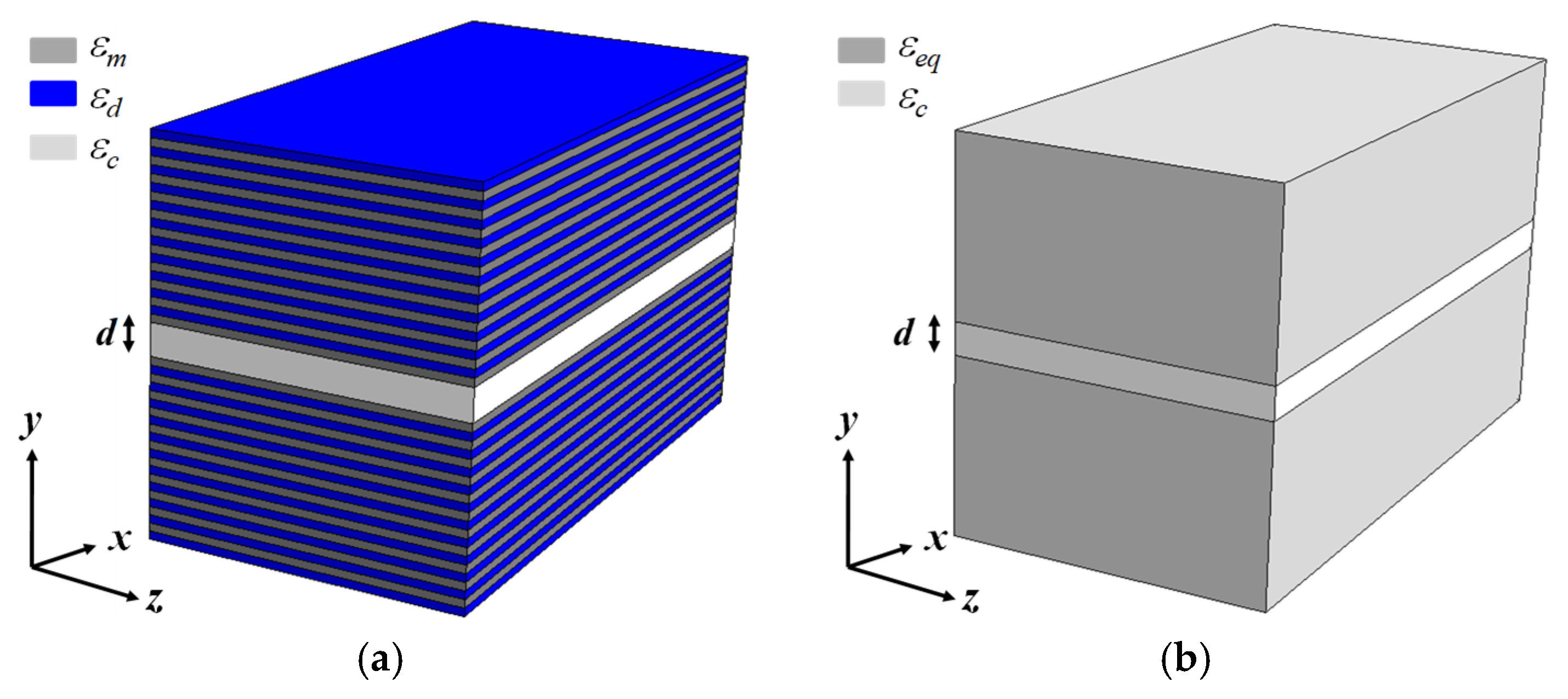
Figure 1a is a schematic view of the planar HIH-WG, and
Figure 1b is the equivalent EMT model. In order to avoid any confusion and for the sake of simplicity, we assign to
Figure 1b three regions
i = 1, 2, 3 from top to bottom, respectively. The HIH-WG model is described by a few parameters, that is, core width
d and cladding metal filling ratio
between the total metal layer thickness
and dielectric
counterpart. Two basic HIH-WGs assemblies are possible. A symmetric one with the same
ri (
i = 1,3) and an asymmetric one with different
ri (
i = 1,3) are used for the upper and bottom claddings. The first device has been extensively analyzed. The last one is considered in this work.
Homogeneous and isotropic insulators have
tensor representation with real and positive
εc components. On the other hand, the HMM tensor model has
and uniaxial symmetry, that is, equal parallel
and perpendicular
interface components. The relationship between
εm,
εd, and HMM tensor components arises from the EMT approach. Here, the propagation geometry assumes surface plasmon polariton (SPP) waves propagating in the
x direction and no spatial variation in the in-plane
z direction
. For our 1D problem, the SPP wave has a parallel propagation constant
and perpendicular
(
i = 1, 2, 3) interface wave vector components. Employing
and
notation, the uniaxial HMM tensor
component reads [
20,
31]:
If we select different HMMs for
Figure 1b, in three layers, the dispersion relationship for this full HMM-WG reads [
3,
9,
10,
11,
12]:
with the implicit relation
(
i = 1, 2, 3) connecting
ky,i and
kx appearing above [
3,
9,
10,
11,
12]. The general form of Equation (2) (and
ky,i) will be the sources of desired relations, as follows.
Asymmetric HIH-WG implies
and
in Equation (2) (and
ky,i). Although common, an insulated core not only defines but also makes this choice the better one to study the length propagation over the propagation character of our unusual WG devices. The dispersion relation to be numerically calculated (see
Section 3) reads [
3,
9,
10,
11,
12]:
Symmetric HIH-WGs are expected to perform the following function first. Since no other authors, to our knowledge, explored the asymmetries effects in metamaterial waveguides, we cannot compare our results with previously published works. However, we validated our approach with symmetric waveguides. Symmetric HIH-WGs have another form.
Now
,
at the core and
i = (1,3),
at claddings. Thus, Equation (3) simplifies [
9,
10,
11]:
A direct measure of energy decrease in the direction of propagation is defined as . This formula also reveals, via kx, the physical meaning of L dependence with regard to d, r, and WG parameters. As already explained, the propagation length L will be used to gauge the performance of the asymmetry effects in HIH-WG devices. A direct measure of the mode profile at the interfaces is defined as . Although out of the main scope of this paper, the penetration depth defined above is another reason why multilayered WG are preferable to the traditional ones.
Metal and insulator experimental optical constants are due to references [
31,
32,
33,
34]. Incident light within 1200 nm ≤ λ ≤ 1700 nm or λ = 1550 nm (C-band telecom standard) midpoint is observed in our simulations. The analysis proceeds with 0.2 ≤
ri ≤1 (
i = 1,3) as well as fixed
r3 or fixed
d WG layouts. HIH-WG cores have
d = 25 nm up to
d = 75 nm, another interval than that used to study both symmetric and asymmetric HIH-WGs [
9,
10,
11]. Smaller
d is in the order of magnitude of the thinnest Au layer that can be deposited on a silica substrate [
22]. Also, we generalize the characterization of asymmetry (
r1≠
r3), selecting different metals for each HMM cladding. The next section is dedicated to looking at some singular
L behavior in these devices.
3. Results and Discussion
We first assume full-asymmetric (
r1 ≠
r3) 0.1 ≤
ri ≤ 1 (
i = 1,3) AgSiO
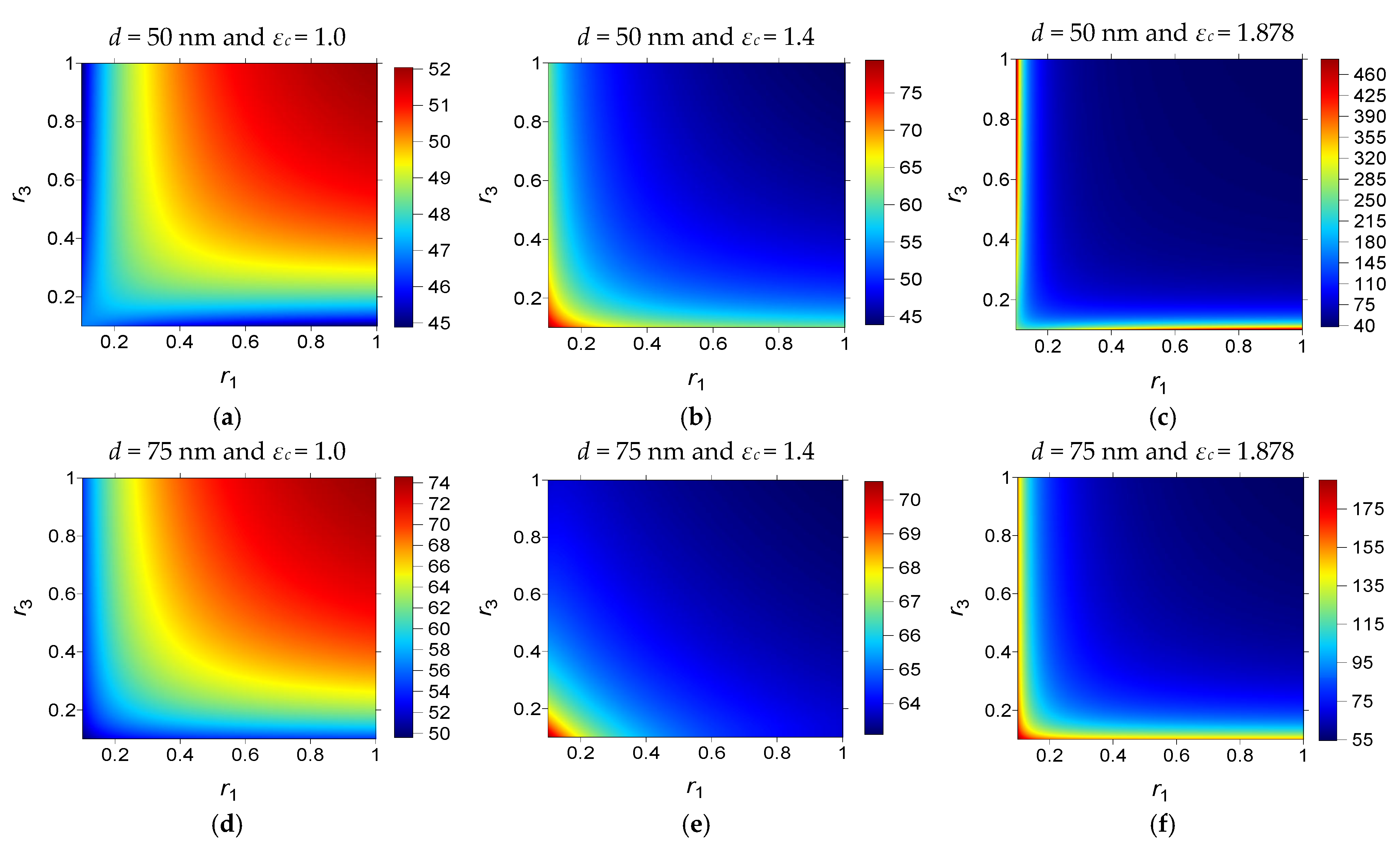
2 HIH-WGs under λ = 1550 nm radiation. Three
εc are considered: 1.0 (a, d), 1.4 (b, e), and 1.878 (c, f) columns with upper rows,
d = 50 nm, and bottom rows,
d = 75 nm in
Figure 2. The figure displays
L dependence on them. We considered in our simulations waveguides with core widths compatible with those found in the specialized literature analyzing metamaterial waveguides operating in the infrared interval of frequencies of about tens of nanometers.
Figure 2 shows that larger
d corresponds to larger
L, regardless of
εc or
ri. Further,
d insensibility (
L constant) occurs when
ri ≥ 0.4 (
i = 1,3) accompanied by
L decreasing as
εc increases. More homogeneous behavior happens in
Figure 2c,f (
εc = 1.878),
ri ≥ 0.2 (
i = 1,3), but with a smaller
L. Thus, fixing
εc and
L operation point, one has HIH-WG designs unveiling the
ri-tolerant devices (λ = 1550 nm).
As
ri goes to unity, a symmetric MIM-WG limiting case arises, usually reducing the propagation length to pay off the dissipative metal presence in the structure. It is easy to see in
Figure 2a,d (
εc = 1.0) that this is not the case for full-asymmetric AgSiO2 HIH-WGs.
In fact, another unexpected feature occurs with L increasing while ri increases, showing the strong correlation between ri, εc, and d that (λ = 1550 nm) light perceives in these structures. Above ri ≥ 0.4 (i = 1,3), a constant L profile is assured for all devices, which always depends on d and εc values.
The next step studies full-asymmetric (
r1 ≠
r3) 0.1 ≤
ri ≤ 1 (
i = 1,3) AuSiO
2 HIH-WGs under λ = 1550 nm radiation.
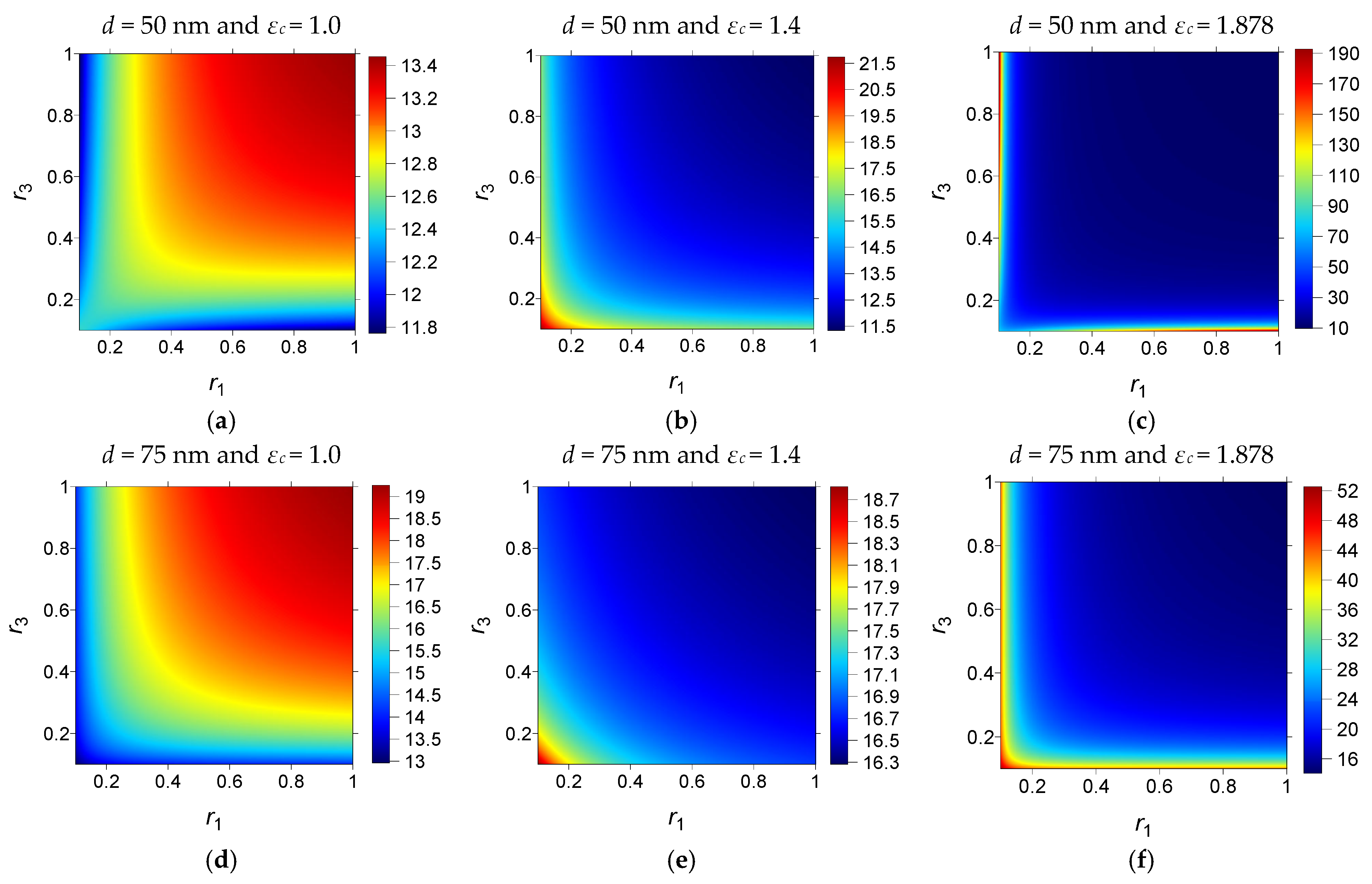
Figure 3 has
εc: 1.0 (a, d), 1.4 (b, e), and 1.878 (c, f) columns with upper
d = 50 nm and bottom
d = 75 nm rows. The figure displays
L dependence on them.
Figure 3 reproduces all the
L behavior displayed in
Figure 2, but with a smaller
L. The more dissipative optical properties of Au than those of Ag reduce the
L propagation length in AuSiO
2 assemblies. Even so, the low chemical reactivity of Au may overcome this unfavorable response in applications like open-air sensor systems [
35]. Nevertheless,
L performance measured in tens of µm always achievable.
Common sense of asymmetry (
r1 ≠
r3) can be generalized in a straightforward manner, taking Au as the upper and Ag as the bottom multilayer metal elements. For the sake of comparison with the WG undergone conventional asymmetry, such a full-asymmetric AgAuSiO
2 HIH-WG was simulated, mirroring (λ = 1550 nm, 0.1 ≤
ri ≤ 1,
i = 1, 3) previous ones. Thus,
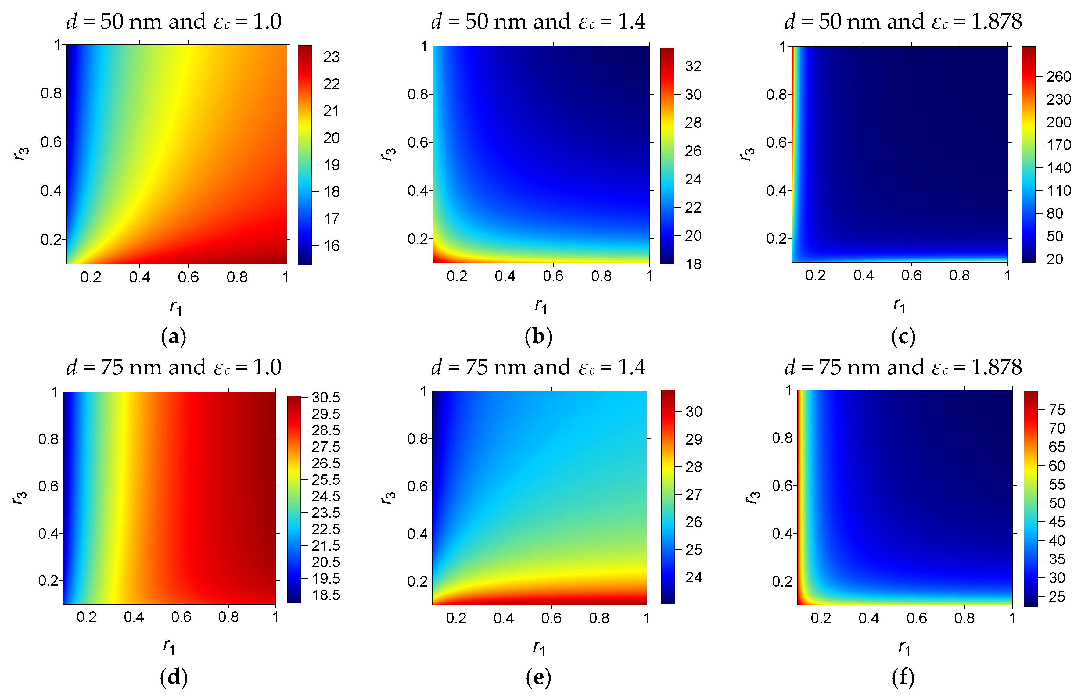
Figure 4 has
εc = 1.0 (a, d), 1.4 (b, e), and 1.878 (c, f) columns with upper
d = 50 nm and bottom
d = 75 nm rows. The figure presents singular
L performances still not discussed.
Figure 4 displays a more involved dependence of
L on
r,
d, and
εc changes. All columns indicate ubiquitous
L increasing as
d increases from the upper to the bottom rows. Simultaneously, all rows indicate
L decreasing as
εc increases from
Figure 4a,d to
Figure 4c,f columns. Whereas better uniformity and insensibility (
L constant) to
ri (
i = 1,3) arises as
εc increases in both
d rows. So, one has new designs unveiling a new
ri-tolerant fabrication issue (λ = 1550 nm). There are a couple of singular behaviors to assert for
L now. Fixing
L and
d operating point,
ri (
i = 1,3) region-free occurs at a narrow (0.7 ≤
ri ≤ 1) or larger (0.4 ≤
ri ≤ 1) range in
Figure 4a,d (
εc = 1.0), and
Figure 4c,f (
εc = 1.878), respectively. Conversely, fixing
εc and
d operating point,
r insensibility (constant
L) profile appears only to specific
r1 interval. As an example,
Figure 4d (
εc = 1.0) presents narrower (0.4 ≤
r1 ≤ 0.7) while
Figure 4f (
εc = 1.878) presents wider (0.4 ≤
r1 ≤ 1) (
d = 75 nm) fabrication tolerance.
Figure 4b,e are clear examples of what a full-asymmetric design can offer. We can see that the mean
εc operating point relates to noticeable equidistant
L behavior.
Planar HMM flexibility now takes the form of restricted structural asymmetry (fixed
d or
r3). Restrict asymmetry 1D architecture is a simple and powerful model employed here to investigate
L spectral response (1200 nm ≤ λ ≤ 1700 nm). Initially, in AgAuSiO
2 HIH-WGs with
r3 = 0.5 (
εm3 =
εAg) as a suitable midpoint of metal presence in the bottom cladding, while 0.2 ≤
r1 ≤1 (
εm1 =
εAu) runs freely.
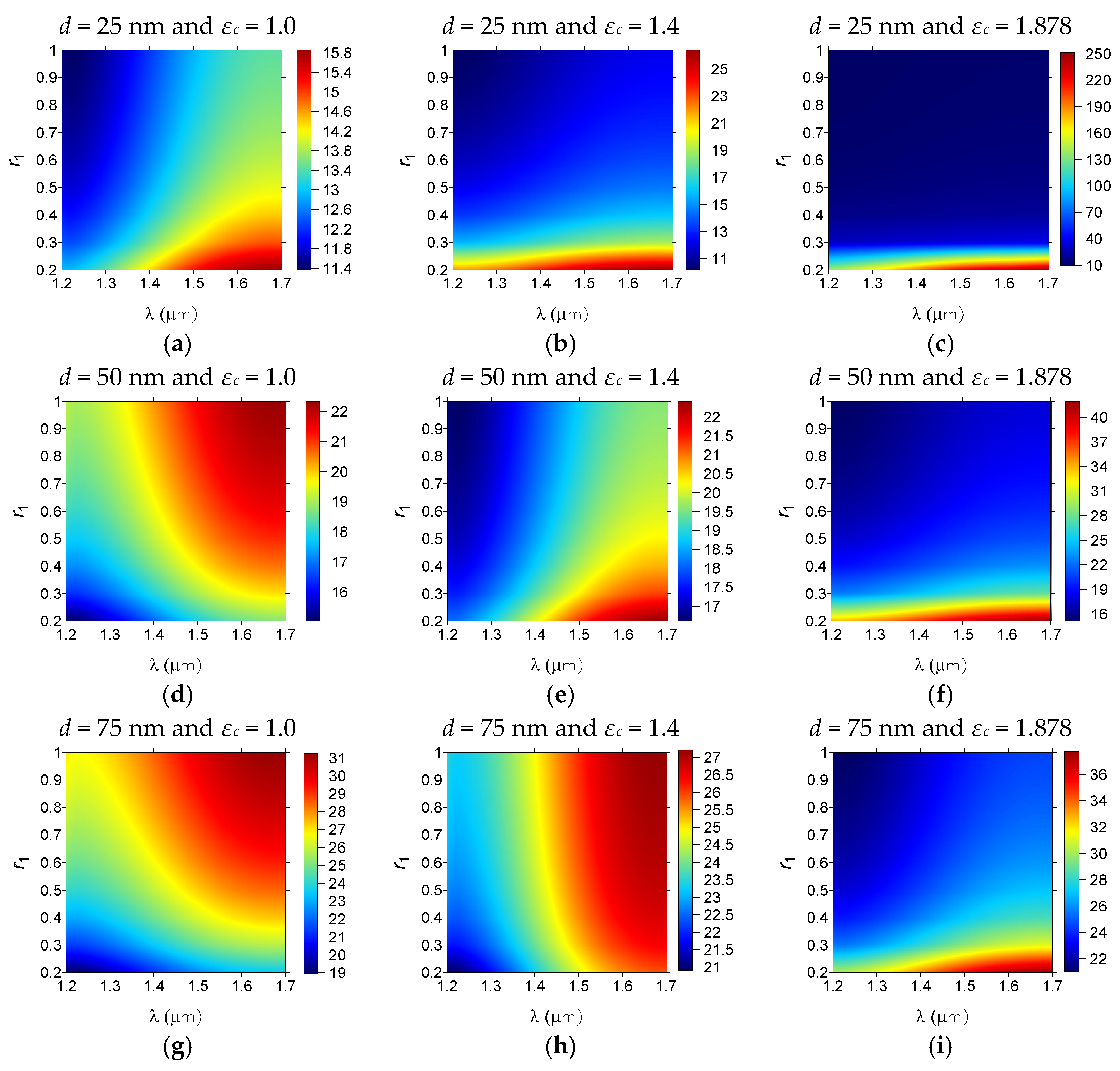
Figure 5 has
εc = 1.0 (a, d, g), 1.4 (b, e, h), and 1.878 (c, f, i) columns with
d = 25 nm,
d = 50 nm, and
d = 75 nm upper, middle, and bottom rows, respectively. In the following, broadband WGs can operate over the complete optical communications frequencies, covering from 1200 nm to 1700 nm. On the other hand, narrowband will maintain its propagation characteristics in less than half of the broadband ones.
Above
r1 ≥ 0.4 and λ ≥ 1400 nm,
Figure 5c,f,i (
εc = 1.878) shows HIH-WGs owing to
d insensibility (
L constant) behavior. Regarding λ, this can be thought of as broadband devices. In contrast, under specific
d and
εc operating point,
Figure 5a,d,g (
εc = 1.0) and
Figure 5b,e,h (
εc = 1.4) show narrowband ones above
r1 ≥ 0.5. For example (
εc = 1.4,
d = 50 nm), operating pointing defines a constant
L profile HIH-WG to λ ≥ 1500 nm radiation. Others’ narrowband designs result from choosing a new (
εc = 1.4,
d = 75 nm) operating point. This way,
L = 25 µm (1550 nm ≤ λ ≤ 1600 nm) or
L = 30 µm (λ ≥ 1600 nm) behavior takes place. As always,
L performance has deeply dependence on
r1, λ, and
εc parameters.
Restrict asymmetry also applies to AuAgSiO
2 HIH-WG,
r3 = 0.50 (
εm3 =
εAu), bottom cladding, while 0.2 ≤
r1 ≤ 1 (
εm1 =
εAg) runs freely, maintaining λ of the previous regime.
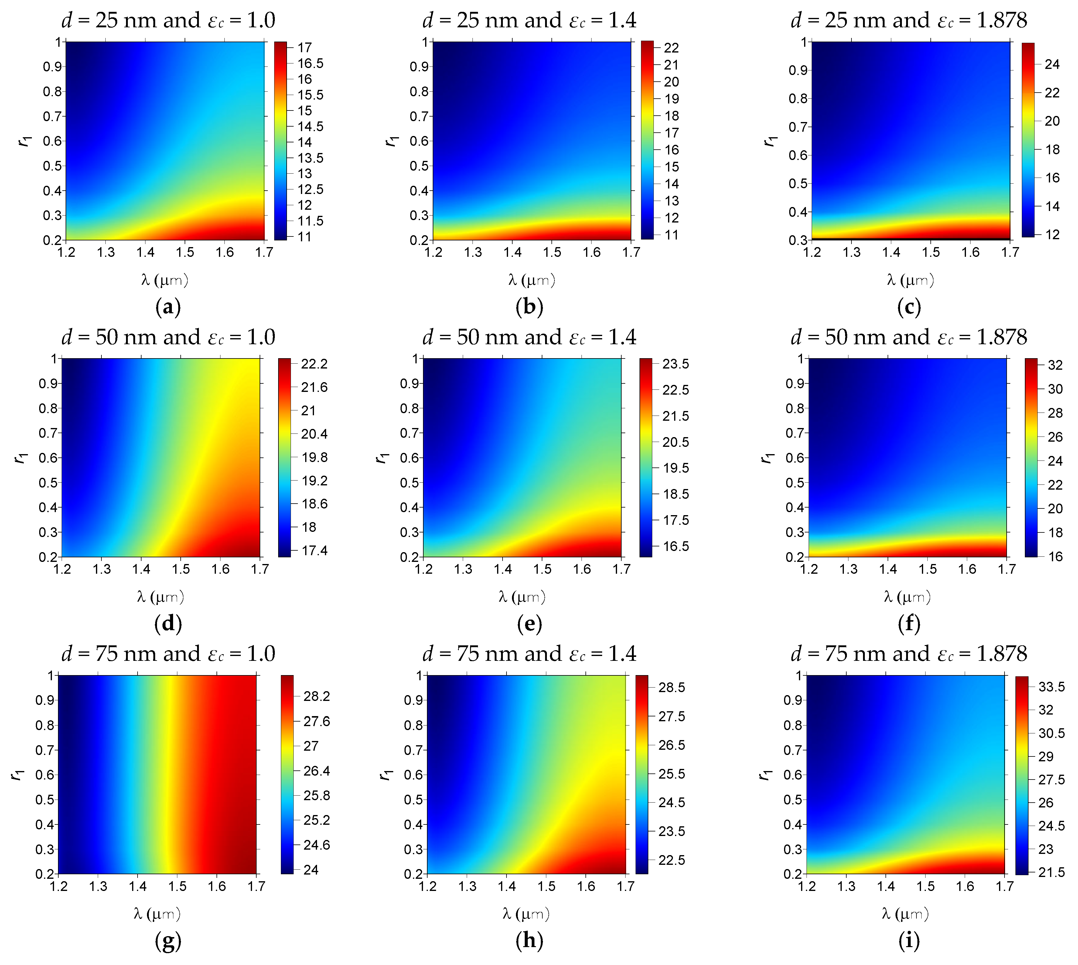
Figure 6 has
εc = 1.0 (a), 1.4 (b), and 1.878 (c) columns with
d = 25 nm,
d = 50 nm, and
d = 75 nm upper, middle, and bottom rows, respectively.
Figure 6c (
εc = 1.878) and
Figure 6b (
εc = 1.4),
d = 25 nm single
r1 ≥ 0.5, λ ≥ 1450 nm regions, define HIH-WGs owing to
d insensibility (
L constant) response. Regarding λ, these designs can be thought of as broadband devices. In contrast,
Figure 6a,d,g (
εc = 1.0) as well as
Figure 6e,f (
εc = 1.4) (
d ≥ 50 nm) displays a constant
L profile only above
r1 ≥ 0.4, always in narrow λ intervals (see
Figure 6g,
d = 75 nm). So we have a set of narrowband HIH-WGs to complete a wide selection of
L performances that the planar HIH-WG project makes possible. At different
L levels,
Figure 6 reproduces what
Figure 5 displays.
Another way to explore restricted asymmetry in WGs takes a fixed
d = 30 nm, for example, with different
εc,
r3 pairs, while 0.1 ≤
r1 ≤ 1 runs freely.
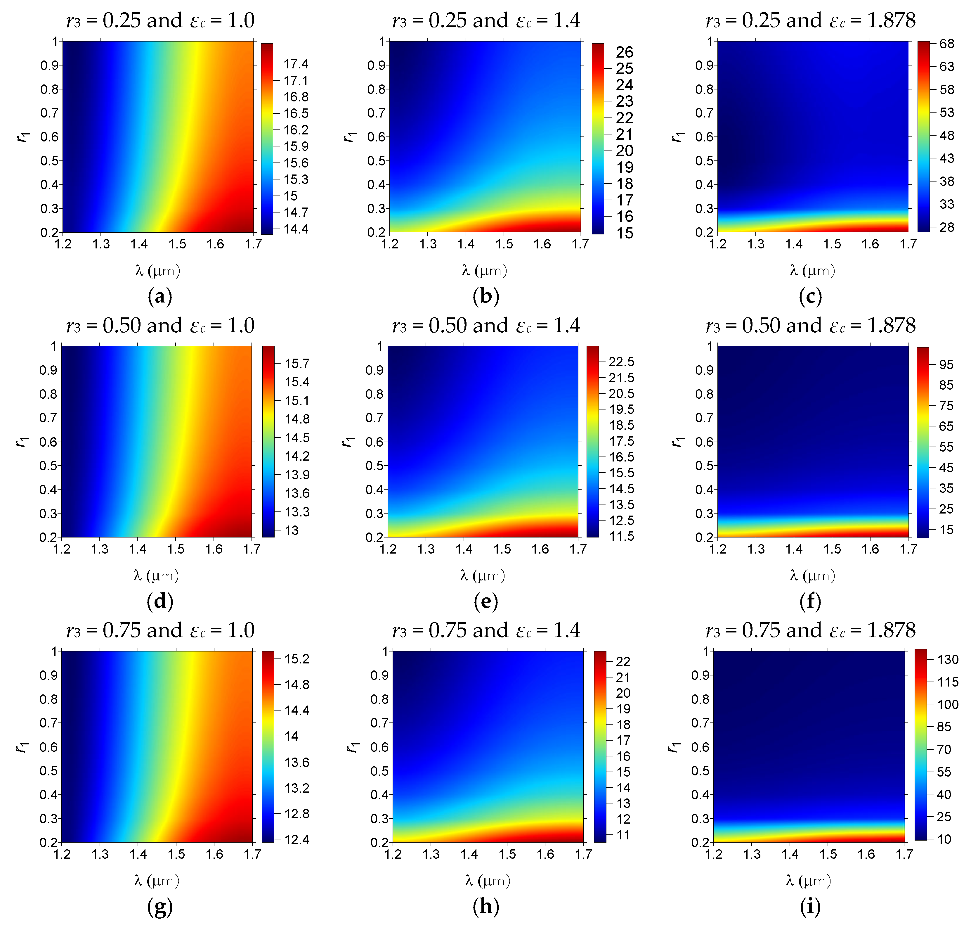
Figure 7 has
εc = 1.0 (a, d, g), 1.4 (b, e, h), 1.878 (c, f, i) columns crossing
r3 = 0.25,
r3 = 0.50,
r3 = 0.75 upper, middle, and bottom rows, respectively. Simulated
L spectral response (1200 nm ≤ λ ≤ 1700 nm) results for AgAuSiO
2 HIH-WG with new structural condition are shown in
Figure 7.
Figure 7c (
εc = 1.878) and
Figure 7b (
εc = 1.4) single
r1 ≥ 0.4, λ ≥ 1350 nm regions, define HIH-WG owing to
r3 insensibility (
L constant) response. Regarding λ, these designs can be thought of as broadband devices. In contrast,
Figure 7a,d,g (
εc = 1.0) (
r3 ≥ 0.25) only displays
L constant profile above
r1 ≥ 0.3 always in narrow λ intervals (λ ≥ 1550 nm). These designs can be thought of as narrowband devices. Restrict asymmetry fixed
d shows better
L performance HIH-WGs than fixed
r3 ones. Finally, the asymmetry
d = 30 nm AuAgSiO
2 HIH-WGs (
εm3 =
εAu) was simulated using identical parameters describing the last structures. Thus,
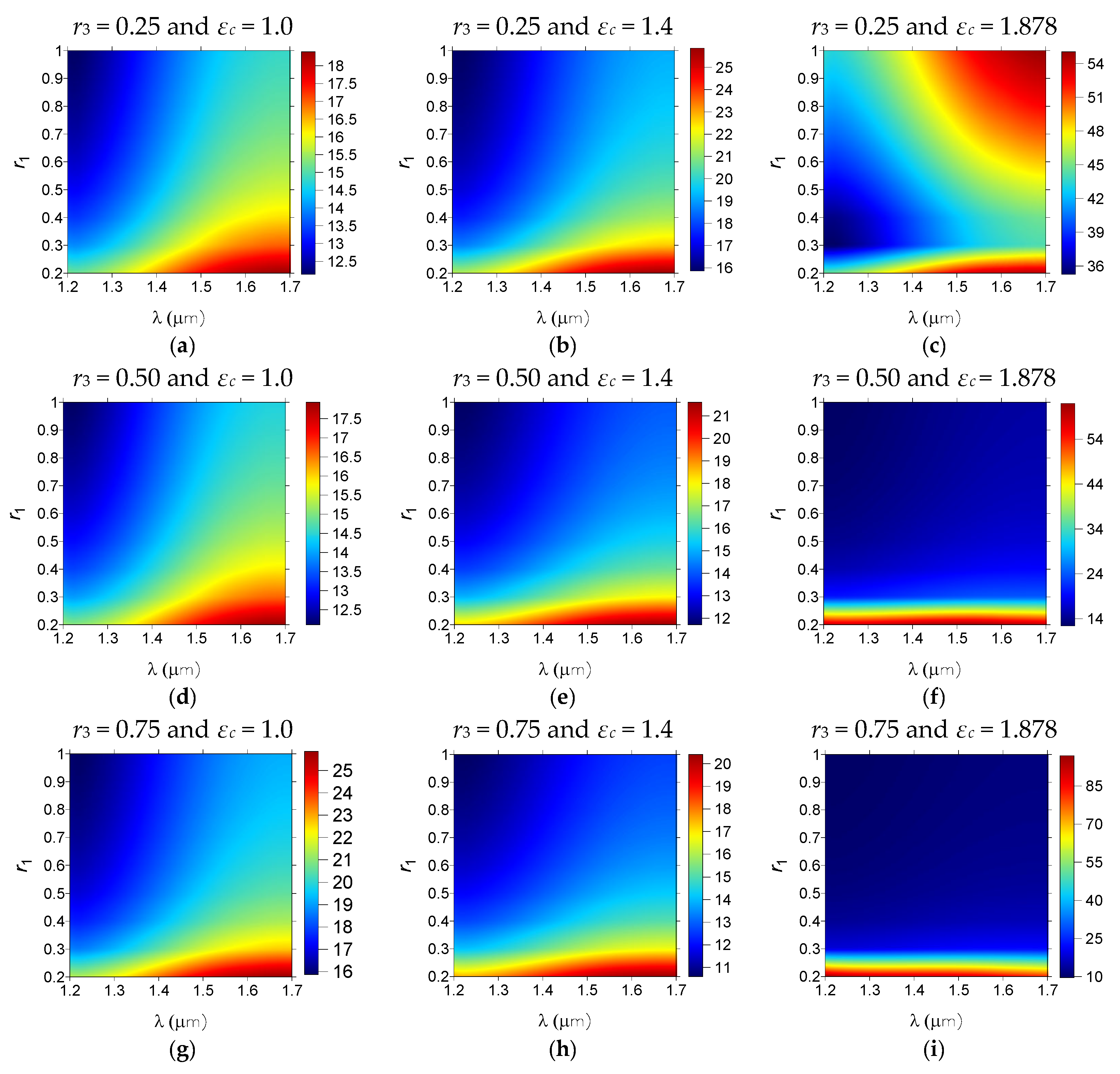
Figure 8 has
εc = 1.0 (a, d, g), 1.4 (b, e, h), 1.878 (c, f, i) columns crossing
r3 = 0.25,
r3 = 0.50, and
r3 = 0.75 upper, middle, and bottom rows, respectively.
Figure 8f,i (
εc = 1.878) HIH-WG owing to
r3 insensibility (
L constant) response. With regards to λ, only these designs can be thought of as broadband devices. The other ones only show the
L constant profile in narrow λ and
r1 intervals. So, restrict asymmetry
d = 30 nm AuAgSiO
2 HIH-WGs are essentially narrowband devices, at least in the interval of 1200 nm ≤ λ ≤ 1700 nm illumination.
Figure 8 corroborates that fixed
d asymmetry HIH-WGs have better
L performance than fixed
r3 similar designs.
4. Conclusions
This work introduces a new class of planar fully asymmetric HIH waveguides for engineered light propagation in integrated photonic systems. Driven by rapid progress in nanometric thin-film fabrication, hyperbolic metamaterials (HMMs) have become powerful platforms for extreme dispersion engineering and subwavelength control of light. Within this context and based on an effective medium theory (EMT) description of multilayer optical media, we extend the notion of asymmetry beyond structural imbalance in the cladding to include the intrinsic field asymmetry of dielectric slab waveguides, establishing full asymmetry as a unified design principle.
Our results demonstrate that this generalized asymmetry provides a highly effective route to tailor and significantly enhance propagation performance. Fully asymmetric HIH waveguides exhibit strongly tunable modal behavior, enabling propagation lengths approaching 400 µm across the C-band of optical telecommunications in optimized configurations. This level of performance highlights the potential of asymmetric metamaterial engineering as a robust strategy for overcoming traditional trade-offs between confinement and loss.
Overall, in the analyzed waveguides, we can observe long propagation distances even in configurations different from the MIM waveguide. Traditional MIM waveguides suffer from energy dissipation, and the propagation relies on Surface Plasmon Polaritons (SPPs) bound to metallic boundaries, where continuous field penetration into the metal causes Joule heating and ohmic losses, and their operating frequency is highly related to the plasmon resonances of the metals used in their composition, on the other hand [
8,
9,
10].
The proposed asymmetric metamaterial claddings can be built using hybrid low-loss systems, considering material combinations including polymers with charge concentrations to shape the propagating mode size and confine the light, reducing losses. This structural optimization extends propagation lengths by orders of magnitude [
8].
Integrated optics usually faces a trade-off between mode size, mode shape, and propagation loss. Asymmetric metamaterial claddings break this constraint through engineered anisotropy. This artificial anisotropy reduces the evanescent skin depth, forcing the fields to decay almost instantly at the core-cladding boundary. As a result, the optical mode remains within a subwavelength core even when its core dimensions are a fraction of the operating wavelength, achieving the ultra-compact footprint of MDM guides without the loss penalty [
8,
10].
Metamaterial waveguides can exhibit the same propagation properties over a large interval of frequencies (broadband operation) and can overcome MDM waveguides’ limitations imposed by the narrow plasma frequency window of native metals. This may cause strong dispersion, localized resonance peaks, and a restricted operational bandwidth. The presence of metamaterial claddings overcomes this because their optical response is governed by subwavelength geometric patterning rather than rigid atomic resonances. This results in waveguides with a highly uniform, flat spectral response that spans all the optical communications Windows covering the O-E-C-L-U bands.
Metamaterial waveguides also open the possibility of obtaining dynamic tunability. Once fabricated, the dielectric properties of native metals in MIM setups are completely fixed. Metamaterial configurations, however, can integrate stimuli-responsive materials such as graphene monolayers, phase-change materials, or liquid crystals into their subwavelength gaps. Applying an external bias voltage alters the carrier density of these embedded layers, dynamically reconfiguring the tensor properties of the asymmetric cladding. This grants real-time control over the waveguide’s effective refractive index, group velocity, losses, and polarization states on a single chip [
18,
21,
27]. In addition, the metamaterial-cladded waveguides can support both TE and TM Modes simultaneously.
The most critical advantage of a metamaterial-cladded waveguide over MIM architectures is polarization versatility. In subwavelength MIM channels, the parallel metallic boundaries force the electric fields parallel to the plates to vanish. Consequently, MDM waveguides block Transverse Electric (TE) waves and only guide Transverse Magnetic (TM) plasmonic modes. Metamaterial claddings do not act as infinite electron pools, meaning they do not short out transverse electric fields. allowing the waveguide to support both TE and TM modes concurrently, allowing applications for on-chip polarization division multiplexing and complex polarization routing [
21].
Finally, the introduction of asymmetry results in an additional degree of freedom to design and tailor the propagation properties of the metamaterial waveguides, adjusting the mode size and mode shape.