All articles published by MDPI are made immediately available worldwide under an open access license. No special
permission is required to reuse all or part of the article published by MDPI, including figures and tables. For
articles published under an open access Creative Common CC BY license, any part of the article may be reused without
permission provided that the original article is clearly cited. For more information, please refer to
https://www.mdpi.com/openaccess.
Feature papers represent the most advanced research with significant potential for high impact in the field. A Feature
Paper should be a substantial original Article that involves several techniques or approaches, provides an outlook for
future research directions and describes possible research applications.
Feature papers are submitted upon individual invitation or recommendation by the scientific editors and must receive
positive feedback from the reviewers.
Editor’s Choice articles are based on recommendations by the scientific editors of MDPI journals from around the world.
Editors select a small number of articles recently published in the journal that they believe will be particularly
interesting to readers, or important in the respective research area. The aim is to provide a snapshot of some of the
most exciting work published in the various research areas of the journal.
This paper presents the procedures employed for experimental functional and performance characterization of a 2 × 2 pixel prototype detection system tailored specifically for the X and Gamma-ray Imaging Spectrometer (XGIS) instrument onboard the THESEUS mission. The XGIS system comprises of two coded masked wide field cameras integrated with monolithic SDDs (Silicon Drift Detectors) and CsI:Tl (Thallium doped-Cesium Iodide) scintillators, contributing to its broad X and -ray detection range. Given the space instrumentation complexity, thorough requirement qualification and testing procedures are essential. This work focuses on working principle, the testing setup utilized, and observed performance for the small scale four-pixel XGIS prototype. Furthermore, the alignment of light output performance of the four-pixel SDD and scintillator prototype detection system with the XGIS instrument requirements is emphasized.
With the scientific goals of exploring the early Universe and advancing next-generation multi-messenger and time-domain astrophysics, the Transient High-Energy Sky and Early Universe Surveyor (THESEUS) aims to build a comprehensive sample of high-redshift () Gamma-Ray Bursts (GRBs) from the first billion years and to conduct an unprecedented deep monitoring of the X-ray transient sky [1,2].
Currently in M7 Phase A study under the European Space Agency (ESA) Cosmic Vision Program, THESEUS is a multi-instrument space mission concept with an intended launch in 2037. Its observational capabilities rely on autonomous rapid slewing, enabling swift transient localization and follow-up.
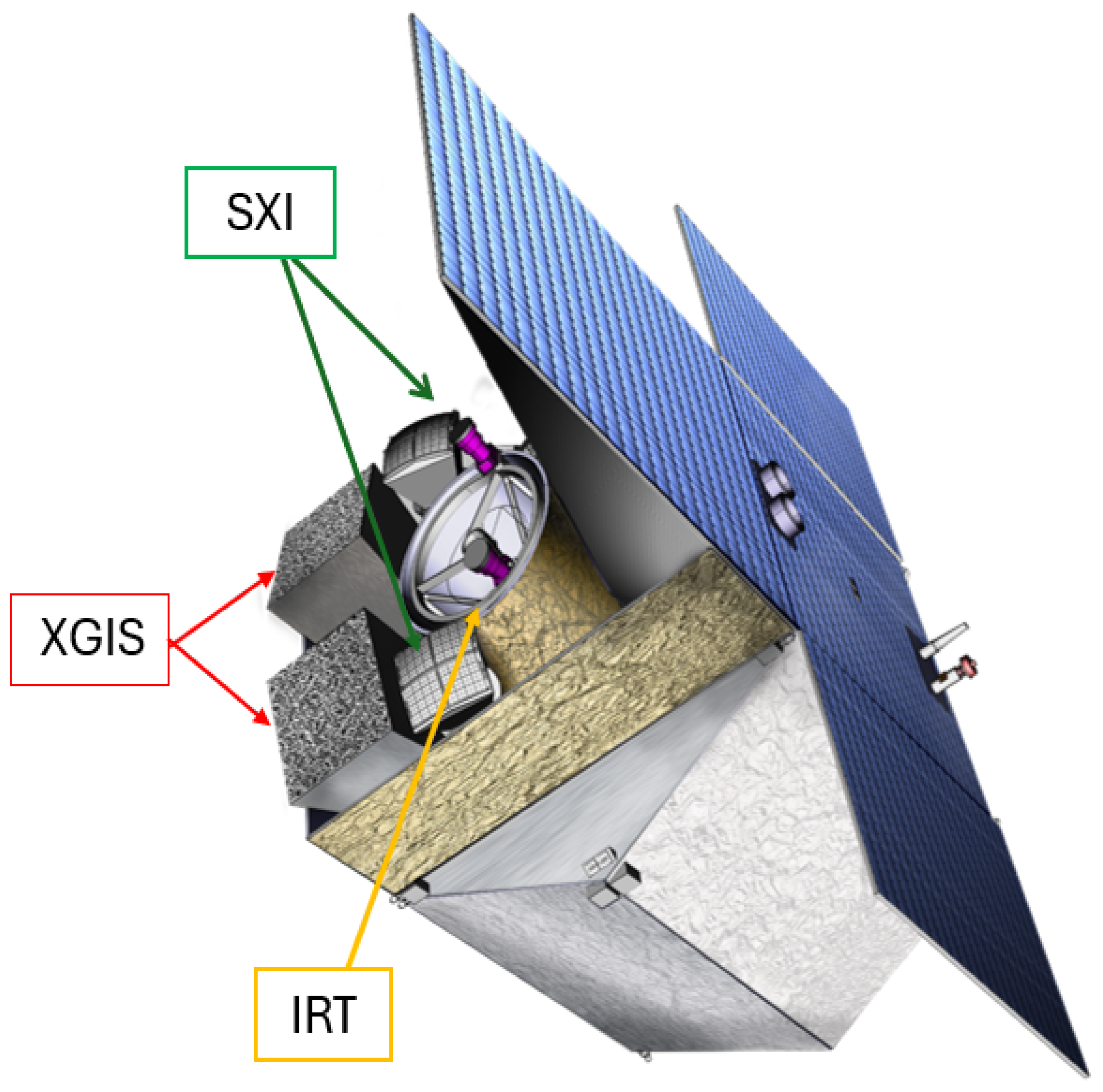
Fulfillment of these scientific objectives will be enabled through three core instruments, equipped with state-of-art technologies, operating in synergy across a wide energy and wavelength range (see Figure 1). The Soft X-ray Imager (SXI), with high positional accuracy (≤2 arcmin), provides rapid transient focusing and imaging capabilities in the soft X-ray band (0.3–5 keV) [3,4]. The imaging capability is further extended in the energy range 2–150 keV with the X- and Gamma-ray Imaging Spectrometer (XGIS), which additionally provides spectroscopic capabilities in the energy ranges up to 10 MeV. Finally, the InfraRed Telescope (IRT; 700–1800 nm) enables transient identification and redshift determination with sub-arcsecond localization accuracy [4]. The XGIS instrument is described in the following section.
2. The XGIS Instrument
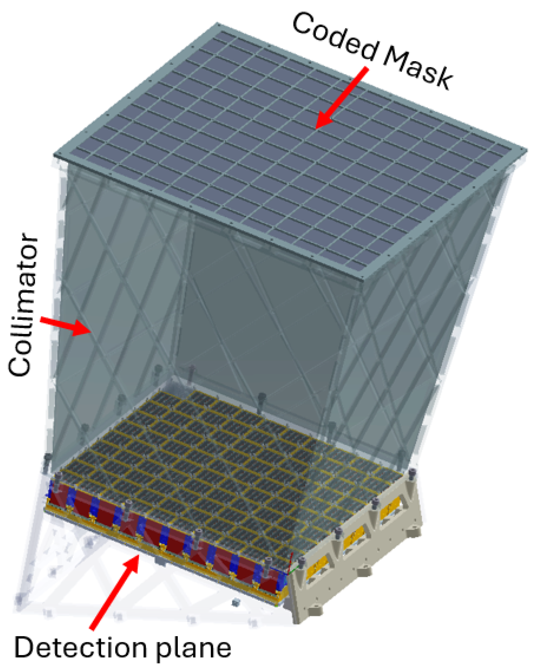
The XGIS is the primary transient monitoring instrument on board the THESEUS spacecraft [5,6]. The mechanical architecture of the XGIS system mainly comprises two Power Supply Units (XSUs), one Data Handling Unit (DHU), and two identical cameras tilted with respect to the spacecraft axis resulting, in a partially overlapping Field of View (FoV) [4]. Figure 2 shows the conceptual mechanical design of an XGIS camera.
Based on the conventional coded aperture mask technique coupled with a position sensitive detector, the XGIS cameras offer imaging capabilities up to 150 keV, with a partially coded FoV and a total FoV of , fully encompassing the FoVs of SXI and IRT. In the 2–150 keV band, with an angular resolution of 60 arcmin, these cameras are capable of detecting localizing high-redshift GRBs and other high-energy transients (Signal to Noise Ratio > 7), with a source localization accuracy of ≤7 arcmin [4]. For incoming photons with energies above 150 keV and up to 10 MeV, each camera is designed to operate as a full-sky spectrometer.
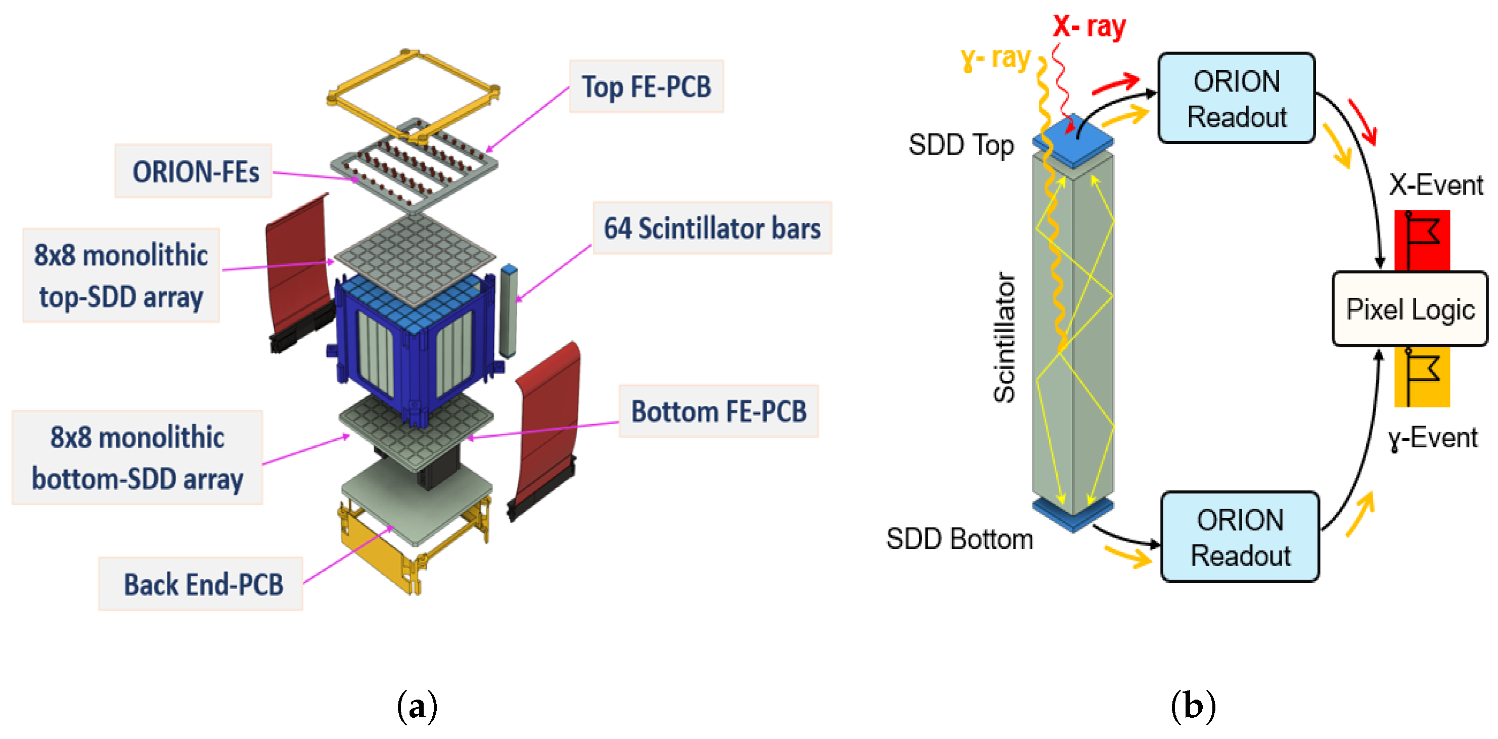
The detection plane of each XGIS camera is modular, consisting of 100 independent and identical XGIS detection modules. These detection modules are further arranged in a array as supermodules, with each camera consisting of 10 supermodules. Each XGIS detection module (Figure 3) as a fundamental unit consists of two highly segmented arrays of 450 μm thick 8 × 8 monolithic SDD matrices, with each SDD corresponding to a cross-section area of 5 × 5 mm2 for direct X-ray detection and 30 mm long 64 CsI:Tl scintillators with a cross section of 4.5 × 4.5 mm2 for the indirect detection of -ray events.
Siswich Principle
Each XGIS pixel incorporates two low-noise SDDs, placed on top and bottom with a 30 mm long CsI:Tl scintillator bar sandwiched in between. The SDDs serve a dual role, functioning as direct detectors for low-energy X-rays (≤∼30 keV) absorbed in the top SDD, and as photodetectors for the scintillation light produced by higher-energy radiations (20 keV upto ∼5 MeV) interacting in the scintillator bar, detected in both the top and bottom SDDs.
This siswich configuration shown in Figure 3b, coupled with specifically designed low-noise ORION Front End (FE) and Back End (BE) electronics to process the charges collected at the SDD anodes, provides a large effective area and μs timing resolution, covering both the low-energy X-ray and γ-ray ranges across a wide energy range in a compact design [6]. Furthermore, the ORION ASIC readout architecture is capable of distinguishing the X and γ events based on the SDDs actively detecting them [8,9,10].
Due to the fully depleted volume and extremely small output anode size that collects the electrons produced, SDDs feature a very low device capacitance (∼tens of fF) [11]. Hence, in combination with optimally designed FE readout electronics, they offer low electronic noise, low energy X-ray thresholds and high energy resolution in energy ranges upto ∼30 keV. High sensitivity in ranges up to ∼5 MeV is extended through CsI:Tl bars with an emission peak at 550 nm and a high scintillation light output of ∼52,000 photons/MeV [12,13]. With 100 64-pixel XGIS modules as a whole detector and time-coincident Compton interactions across multiple pixels, higher energy ranges up to 10 MeV are attainable through signal reconstruction and post-processing. To operate with siswich architecture, the XGIS must ensure a reliable energy overlap between maximum detectable X-ray energies and minimum detectable ray energies, to provide complete coverage in the 2 keV and 10 MeV energy band. Therefore, XGIS performance requirements defined in the framework of the ESA Phase A study specify that each pixel shall achieve a minimum effective Light Output value of 25 /keV at 662 keV at both the Beginning Of Life and End Of Life (BOL/EOL) of its operational lifetime.
3. Methodology and Experimental Characterization: SDD–ORION IV and SDD–Scintillator–ORION IV System
Given the dual-detection functionality inherent to each pixel, the characterization process requires the simultaneous assessment of both detector types within a unified testing environment. This requires a methodological approach that ensures an accurate evaluation of detector performance across the entire operational energy range, providing critical insights necessary for optimizing instrument sensitivity and overall mission reliability. Therefore, the experimental setup and performance characterization process utilized for the XGIS instrument to comprehensively test two distinct detection technologies combined within a four pixel module are discussed.
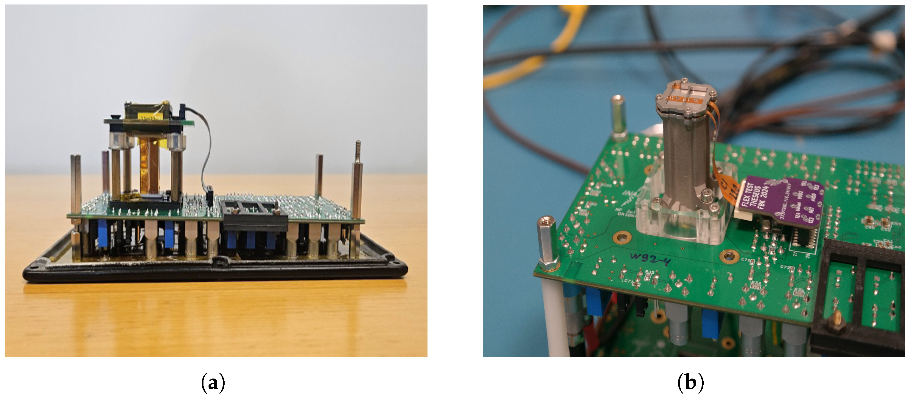
Manufactured in 2020, the four-pixel ORION ASIC prototypes with the complete FE and BE chipsets bonded to 2 × 2 SDD arrays were first tested and reported at INAF-OAS Bologna, Italy, for their functionality and performance in 2023 [7]. In 2025, an extended evaluation was performed on these prototypes with 4 CsI:Tl bars, optically coupled with 2 × 2 top and bottom SDD matrices (shown in Figure 4a). These experimental activities have been performed in collaboration with INAF-OAS Bologna and Fondazione Bruno Kessler (FBK), Trento. The performance tests reported here have been conducted on the ORION IV prototypes, designed by the Politecnico di Milano in collaboration with the University of Pavia, assembled in a reduced prototype of 4 pixels fully representative of the XGIS design (see Figure 4b). Utilizing only the analogic chain of the FE and BE circuitory, these scintillator-equipped prototypes were characterized specifically for their light output performances. The aim of the tests performed was to verify the pixel functionality concept described in the subsection Siswich Principle and characterize the performance, taking into consideration the assembly method for the XGIS detectors. The XGIS detectors, assembled in a unique configuration with long and narrow scintillator crystals, require a specific mode of testing to define a system that is independent of the point of interaction of energy events along the scintillator length. As an XGIS detection plane will be composed of thousands of pixels that should be manufactured and tested, a simple and complete test methodology along with pixel compatibility parameters should be defined. Some compatibility parameters to define the suitability of the pixels can be assessed in terms of the electronic noise of the system, the energy resolution from the SDDs, and the scintillator light output.
The availability of the analogue shaped output from the ORION BE enables the evaluation of these pixel parameters with an on-chip Analog to Digital Converter (ADC) or utilizing an external ADC for the signal processing.
The first step of the characterization process involves testing the SDD-ORION IV prototype using the 241Am and 55Fe radioactive sources and with artificial electrical voltage impulses supplied directly to the ORION ASIC preamplifier via a test capacitance. The system calibration for parameters such as the gain, offset, and linear operating range can be performed through the known test capacitance value, utilizing the acquired voltage impulses and radioactive sources spectra [7,8]. The experimental performance results of the SDD-ORION IV system, along with the test capacitance value of ∼18 fF, have been calculated and reported in previous works. Based on the capacitance measurements performed on several ORION test capacitors, the observed variation with respect to 18 fF is approximately ±1.6%. These performance estimations include an energy resolution of 434 eV Full Width at Half-Maximum (FWHM) at 13.7 keV 241Am peak, ∼44 electrons r.m.s electronic noise at 5.9 keV 55Fe peak for the X-processing branch, and ∼75 electrons r.m.s. at 59.6 keV 241Am peak for the top and bottom-processing branches measured individually at room temperature [7]. The four-pixel SDD-ORION IV prototype with complete FE and BE chipsets, including on-chip ADCs, was utilized for this experimental performance estimation at INAF-OAS Bologna.
Utilizing the calibration and performance parameters obtained, the SDD–Scintillator–ORION IV system shown in Figure 4b has been tested by irradiating the scintillator bar with a 137Cs radioactive source, and the system performance is reported with the Light Output (LO) parameter calculated at the 662 keV photopeak of the 137Cs.
Light Output
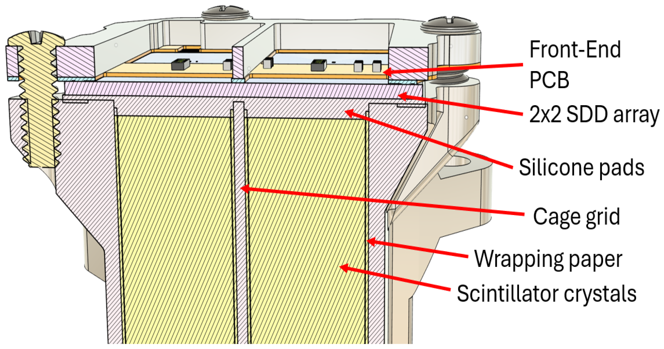
To establish the relationship between the charges collected at the SDD anodes, produced by the scintillation photons due to a given energy deposition from incoming γ-rays in the CsI:Tl scintillators, a calibration procedure is required. Therefore, measurement of the Light Output (LO) parameter, achievable from the 2 × 2 XGIS prototype is necessary. Unlike the performance evaluation of SDD system reported above, the LO performance of the SDD–Scintillator detection system depends on the quality of the optical contact, the reflective material wrapping for the scintillators, and the scintillator crystal size and material. Therefore, preparation of this detection system has been realized in several steps in collaboration with FBK Trento. Figure 5 shows the mechanical design adapted as the preliminary development step for the realization of the four-pixel SDD–Scintillator assembly.
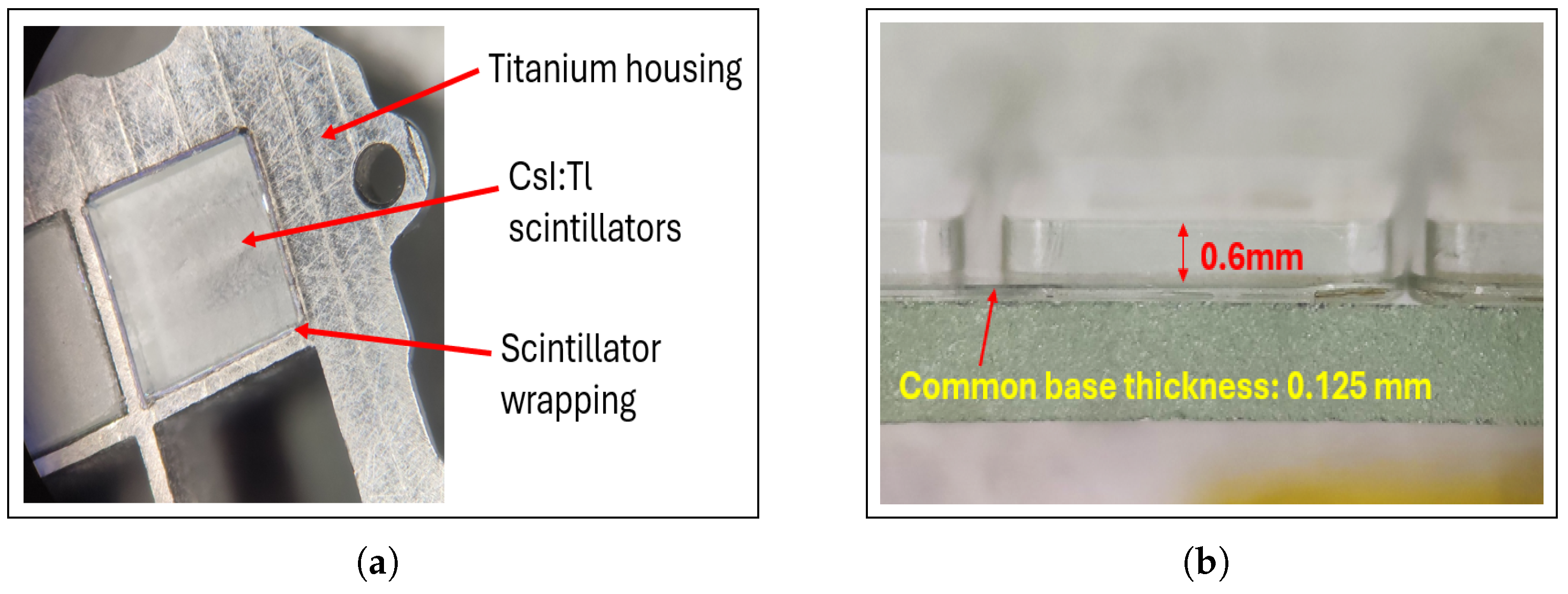
Four 30 mm long CsI:Tl scintillators were placed inside an custom-designed titanium housing, as shown in the left panel of Figure 6. The housing design is geometrically the same as the full size 8 × 8 XGIS module. The channels in the housing are lined with highly reflective VM2000 material, with the size exactly matching the size of the scintillator crystal, to ensure the lateral mechanical stability of the system. The scintillator crystals are slightly shorter than the height of the crystal housing, allowing the optical silicone pads to enter inside the housing, minimizing the possible optical crosstalk between the neighboring channels. The silicone pads used for the optical coupling between SDD and scintillator shown in Figure 6b are fabricated as an array of 0.6 mm high square pads with a lateral cross section matching the scintillator dimensions connected by a very thin 0.125 mm common base. The titanium structure containing the CsI:Tl crystals is optically coupled with the four-pixel SDDs array positioned on the top and bottom sides by means of these silicone pads. Good spectroscopic performance and manufacturing feasibility are the main driving factors for material selection and this component assembly.
Since the LO is a highly variable and position-dependent parameter, when calculated utilizing the charges deposited solely either on the top or bottom SDD anodes, the output signals from the γ-top and γ-bottom processors of the ORION ASIC are summed utilizing an external device. Therefore, the LO performance of the scintillator detection system for a full pixel can be performed without the necessity of collecting signals individually from collimation point by point along the length of the bars. This summed γ signal is further processed for the calculation of the charges deposited at the top and bottom SDDs, ultimately yielding the Light Output values for the detector–scintillation system as a whole.
Thus, to perform the signal adding and processing operations, a top and bottom signal adder, either external or through a virtual oscilloscope setup supplemented with a Multi Channel Analyzer (MCA) for external Analog to Digital conversion can be incorporated externally in the electronic chain.
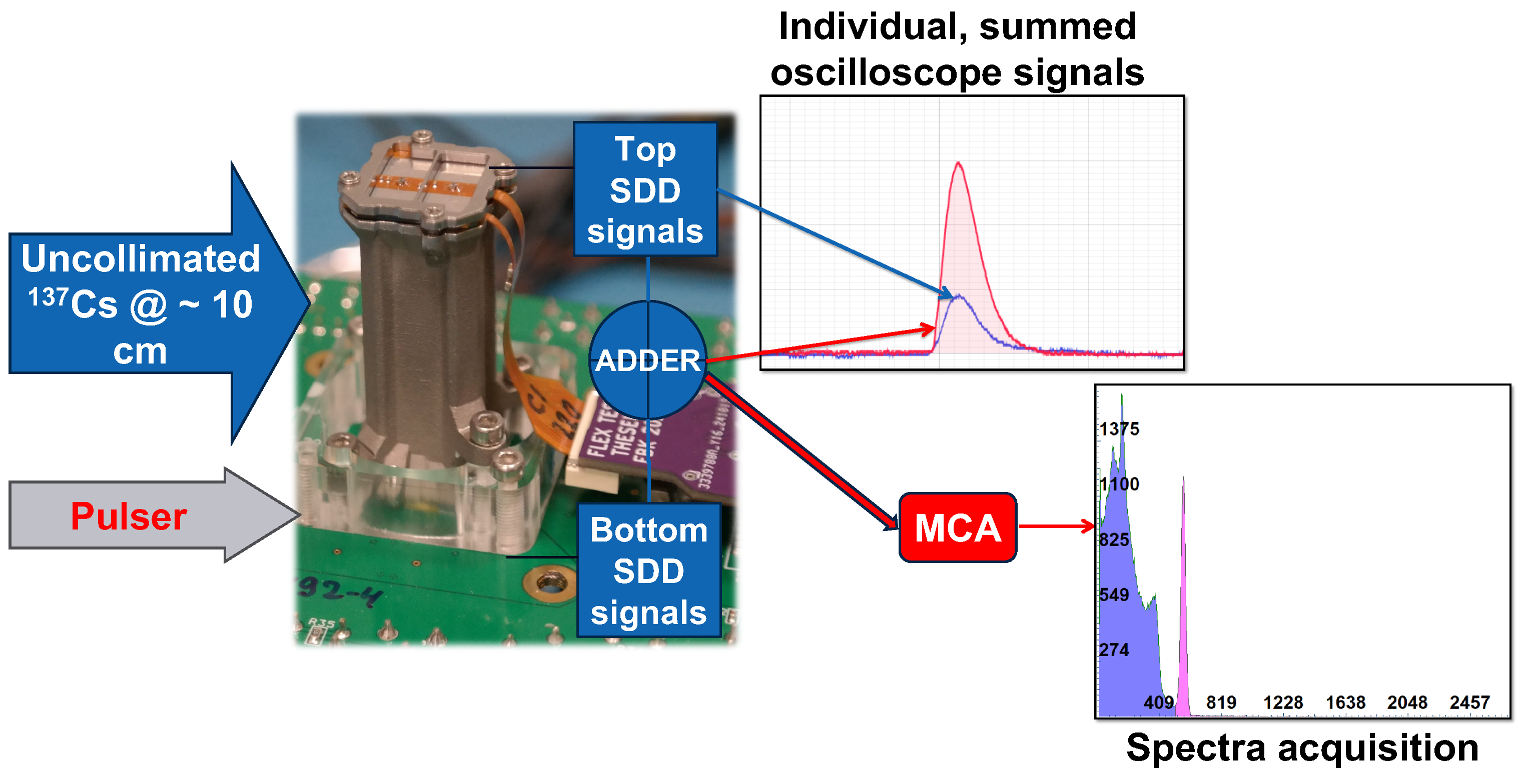
Figure 7 shows the experimental testing chain, with the titanium-housed four-pixel SDD–Scintillator system irradiated with an uncollimated 137Cs source at a distance of 10 cm or stimulated with an artificial voltage supply from DT4800 with an amplitude accuracy of ±0.5% for a set value [14]. The four-pixel detection system, mounted and bonded to the ORION ASIC-FE, is configured to select the required pixel address in shaping mode [7,8,10], through a LabView configuration program. The ORION-FE signals from the top and bottom SDDs are channeled to the respective analog BE γ-top and bottom processors, which are then summed through an externally connected analog signal adder. The summed signal is further supplied to an externally connected Analog to Digital Converter, Amptek MCA 8000D [15]. The final spectrum, demonstrating the variation in radioactive or electrical event counts with respect to ADC channels, is acquired using MCA Digital Pulse Processor (DPP)-based Software.
Given the maximum energy detection limit defined by the SDD thickness (∼30–35 keV), a higher LO value is required from the prototype to reliably maintain the overlap between the X and γ regions with a safe operational margin. A high LO (∼30 /keV), obtained from the summed γ processors signals of the system, ensures the necessary overlap of maximum detectable energy limit for X-rays and minimum detectable γ rays.
The LO calculation of the system requires identifying a relationship between the ADC channel position and the number of electrons deposited by the incoming energy or the test voltages supplied. Therefore, to estimate the relationship between the channel position and electrons, calibration of the γ top or bottom channel is performed by supplying electrical voltage impulses. With the known ORION ASIC test capacitance value ∼18 fF and utilizing the relationship between capacitance C, voltage V, and charge Q,
and the charges for the supplied voltage impulses can be calculated. With the charges calculated in Equation (1), the number of electrons deposited for each impulse can be calculated by Equation (2),
Therefore, with an external MCA-based ADC or an internal ADC-acquired spectra, the relationship between the MCA ADC channels for each test voltage peak and the number of electrons deposited is defined. With three ADC centroid positions of the electrical impulses or radioactive peaks in the acquired spectra, a linear relationship between ADC channels and the number of electrons deposited can be established as follows:
where is the number of electrons deposited, A is the offset, B is the gain, and channel is the ADC peak centroid position. To estimate the system LO, the SDD–ORION–Scintillator detection system should be exposed to uncollimated peak-emitting radioactive sources such as 137Cs for an adequate duration to acquire sufficient event counts. With the known energy photopeaks for such sources, the peak centroid can be calculated from the acquired MCA spectra by selecting the region of interest. This observed peak centroid channel position can be substituted in the defined linear calibration relation 3 to obtain the equivalent number of electrons deposited, . Finally, the LO of a scintillator system can be calculated, as shown in Equation (4),
where is a known emitted photopeak energy of any radioactive source.
Therefore, to evaluate the SDD–Scintillator–ORION IV system response, the four-pixel ORION board bonded to two 2 × 2 SDD matrices with four CsI:Tl scintillator bars was irradiated with an uncollimated 137Cs source at room temperature. Furthermore, artificial electrical test pulse inputs were supplied to the system for voltages equivalent to 100 mV and 200 mV under similar conditions. An overlap of the 100 mV peak and 137Cs photopeak was observed during these combined measurements. Therefore, 100 mV and 200 mV were acquired in a separate spectra and recorded together to evaluate their peak positions for LO calculations. The spectra for both were acquired in shaper mode, measuring each pixel individually, for an interval of 30 min and 10 s, respectively. Configuring the ORION ASIC in shaper mode enables preliminary pre-amplification and shaping of the charge signals obtained from the top and bottom SDDs, followed by signal processing performed by a Charge Sensitive Amplifier (CSA) embedded in the front-end circuitry [7,8,10]. This signal is forwarded by a current conveyor to the second shaping stages of the processor present in the ORION ASIC BE, providing top and bottom analog signals with a shaping time of 3 μs. Analog output waveforms from the complete front-end (FE) circuitry followed by the signal shaping stages in the back end (BE) were acquired through the top and bottom processing chains. The final sampled spectra acquistion has been performed on the sum of the top and bottom signals from the processor and by connecting a digital Amptek Multi Channel Analyzer 8000D [15] in the experimental setup.
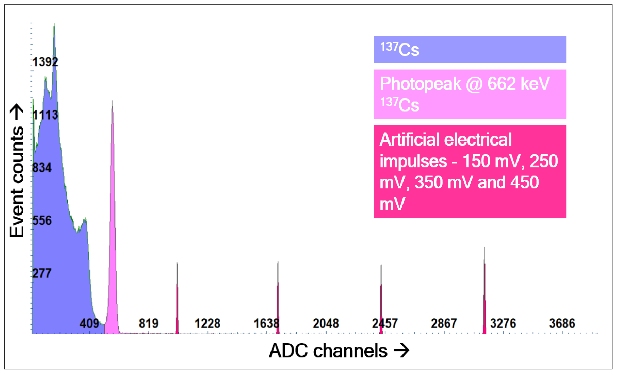
For illustrative purposes, the artificial pulse voltage amplitudes were further increased to 150 mV, 250 mV, 350 mV, and 450 mV and recorded separately with 137Cs. Figure 8 is a representative spectrum to demonstrate the performance of one pixel from this four-pixel SDD–Scintillator–ORION IV system in the presence of 137Cs source, followed by the supply of these high amplitude pulses. The 150 mV, 250 mV, 350 mV, and 450 mV test pulse peaks remain clearly separated from the 137Cs photopeak, aiding a better visualization of this system response. This representative spectrum shows a prominent 662 keV 137Cs photopeak, corresponding to the full energy energy deposition by -rays in the detection system. A Compton continuum is also observed, corresponding to the scattered -rays depositing lower energies in the detector. Furthermore, the spectrum shows a clear Compton edge at the higher energy part of the continuum, corresponding to the maximum energy transferred in the detector during the Compton scattering. The features observed are standard characteristics of -ray interactions and demonstrate a suitable detector response. The measured average energy resolution on the 662 keV photopeak 137Cs is 5.8% Full Width at Half Maximum (FWHM), consistent with the XGIS performance requirement for energy resolution < 6% for 600 keV peak at the End of Life (EOL).
For the LO values reported in Table 1, calculations have been performed utilizing artificial impulses of 0.1 V and 0.2 V acquired separately from the 137Cs spectra. Utilizing the 662 keV photopeak of the 137Cs source and Equation (4), the LO for the total -ray signal through this SDD–Scintillator system has been measured to be approximately ∼30 /keV. Table 1 shows the LO performance, derived combining the uncertainties in the fitted values for both electrical pulses and the 137Cs photopeak (which are below <1%) with the systematic errors introduced by the pulser and the test capacitance, which dominate the overall error. Similar performances have been observed for all four pixels, with a ∼±3% pixel-to-pixel variation in the LO values. The observed variations could be potentially attributed to minor mechanical tolerances or small assembly-related differences between pixels. The impact of this level of non-uniformity is negligible and well within the performance constraints for the final design.
While the analysis of the minimum theoretical event detection threshold from the SDD–ORION IV has previously demonstrated sensitivity equivalent to ∼0.8 keV in the lower X-ray energy ranges [7], the LO values obtained from each pixel of the SDD–Scintillator–ORION IV system show processors reliably reaching lower detectable energy values equivalent to ∼30 keV, substantially overlapping the maximum limits of the linear energy detection range from the X-processing branch for each pixel. Therefore, with the measured LO values of ∼30 /keV at 662 keV, the four-pixel SDD–Scintillator–ORION IV system not only fulfills but also substantially exceeds the XGIS performance budget requirement of 25 /keV at 662 keV, validating its suitability for the final XGIS instrument design.
4. Conclusions
In this work, we report the first experimental performance measurements of the four-pixel SDD–Scintillator–ORION IV detection system investigated in terms of the Light Output. While the methodology focuses on the detailed design and assembly of the detection prototype and its experimental setup, the LO evaluation provides the first quantitative performance assessment of this detection system at the four-pixel level. Utilizing the 137Cs 662 keV photopeak and calibrated electrical test pulses, the LO values of ∼30 /keV were measured for each pixel. With a pixel-to-pixel LO variation of ∼±3%, the absolute value remains well within and fully compliant with the XGIS LO performance requirements.
The experimental setup and characterization procedures adapted demonstrate reliability and reproducibility, producing clear spectra and analyzable data. Crucial parameters for the production and scalability of the XGIS detector, such as the Light Output, can be derived from the experimental spectra obtained. Furthermore, the experimental methodology and system utilized will serve as a quality control tool for the detector components planned to be produced and integrated in the future for the development of the XGIS modules and camera.
Author Contributions
Methodology, S.S., E.D., C.L., L.A., R.C., G.B., P.C., F.F., E.J.M., G.M., A.S., D.N., G.P. and E.V.; Data curation, S.S., E.D. and C.L.; Writing—original draft, S.S., E.D., C.L., L.A., R.C., G.B., E.B., P.C., F.F., E.J.M., G.M., A.S., D.N., G.P. and E.V.; Resources, E.D., S.S. and C.L.; Writing—review and editing, S.S., E.D., C.L., L.A., R.C., G.B., E.B., P.C., F.F., E.J.M., G.M., A.S., D.N., G.P. and E.V.; Supervision, C.L., L.A., R.C. and E.V.; Project administration, E.V., L.A., R.C. and C.L.; Funding acquisition, L.A. All authors have read and agreed to the published version of the manuscript.
Funding
This research was supported by ASI-INAF agreement n.2024-17-HH.0.
Data Availability Statement
The raw data supporting the conclusions of this article will be made available by the author on request.
Acknowledgments
This ESA/M7 Phase-A study of THESEUS and the XGIS instrument in Italy is supported by the ASI-INAF agreement n.2024-17-HH.0. The authors would also like to acknowledge the THESEUS consortium members for their continued participation and contributions.
Conflicts of Interest
The authors declare no conflicts of interest.
References
Amati, L.; O’Brien, P.; Götz, D.; Bozzo, E.; Tenzer, C.; Frontera, F.; Ghirlanda, G.; Labanti, C.; Osborne, J.P.; Stratta, G.; et al. The THESEUS Space Mission Concept: Science Case, Design and Expected Performances. Adv. Space Res.2018, 62, 191–244. [Google Scholar] [CrossRef]
Stratta, G.; Ciolfi, R.; Amati, L.; Bozzo, E.; Ghirlanda, G.; Maiorano, E.; Nicastro, L.; Rossi, A.; Vinciguerra, S.; Frontera, F.; et al. THESEUS: A Key Space Mission Concept for Multi-Messenger Astrophysics. Adv. Space Res.2018, 62, 662–682. [Google Scholar] [CrossRef]
McHugh, M.; Hutchinson, I.; Lerman, H.N.; O’Brien, P.; Willingale, R.; Feldman, C.; Beardmore, A.; Speight, R.; Lodge, A.; Drumm, P.; et al. Development of an imaging system for the THESEUS SXI instrument. In Proceedings of the Space Telescopes and Instrumentation 2020: Ultraviolet to Gamma Ray, Online, 14–18 December 2020; Volume 11444, p. 114448Y. [Google Scholar] [CrossRef]
Fuschino, F.; Campana, R.; Labanti, C.; Amati, L.; Virgilli, E.; Terenzi, L.; Bellutti, P.; Bertuccio, G.; Borghi, G.; Ficorella, F.; et al. The XGIS instrument on-board THESEUS: The detection plane and on-board electronics. In Proceeding SPIE; SPIE: Bellingham, WA, USA, 2020; Volume 11444. [Google Scholar] [CrossRef]
Labanti, C.; Amati, L.; Frontera, F.; Mereghetti, S.; Gasent-Blesa, J.L.; Tenzer, C.; Orleanski, P.; Kuvvetli, I.; Campana, R.; Fuschino, F.; et al. The X/Gamma-ray Imaging Spectrometer (XGIS) on-board THESEUS: Design, main characteristics, and concept of operation. In Proceeding SPIE; SPIE: Bellingham, WA, USA, 2020; Volume 11444, p. 114442K. [Google Scholar] [CrossRef]
Srivastava, S.; Labanti, C.; Amati, L.; Campana, R.; Virgilli, E.; Marchesini, E.; Borciani, E.; Mele, F.; Dedolli, I.; Bertuccio, G.; et al. The XGIS instrument on-board THESEUS: Detector principle and read-out electronics. J. Instrum.2024, 19, C02005. [Google Scholar] [CrossRef]
Mele, F.; Dedolli, I.; Gandola, M.; Grassi, M.; Malcovati, P.; Amati, L.; Bellutti, P.; Borghi, G.; Campana, R.; Demenev, E.; et al. ORION, a Multichip Readout Electronics for Satellite Wide Energy Range X-/γ-Ray Imaging Spectroscopy: Design and Characterization of the Analog Section. IEEE Trans. Nucl. Sci.2021, 68, 2801–2809. [Google Scholar] [CrossRef]
Mele, F. High Energy Resolution X and Gamma Ray Imaging Spectroscopy with the ORION Multichip Readout Electronics; Springer: Cham, Switzerland, 2023; pp. 95–109. [Google Scholar] [CrossRef]
Grassi, M.; Malcovati, P. A Robust and Versatile Analog-to-Digital Converter for Space Exploration Spectroscopy on Satellites. In Proceedings of the 2021 IEEE 6th International Forum on RTSI, Naples, Italy, 6–9 September 2021; pp. 519–523. [Google Scholar] [CrossRef]
Bertuccio, G.; Mele, F.; Gandola, M.; Ahangarianabhari, M.; Macera, D.; Quercia, J.; Shi, Y. Semiconductor Drift Detector’s Anode Capacitance: Measurement in Operating Conditions and Applications in Charge Readout. In Proceedings of the 2022 IEEE (NSS/MIC), Milano, Italy, 5–12 November 2022; IEEE: Piscataway, NJ, USA, 2023; pp. 1–3. [Google Scholar]
Fiorini, C.; Longoni, A.; Perotti, F.; Labanti, C.; Lechner, P.; Struder, L. Gamma ray spectroscopy with CsI(Tl) scintillator coupled to silicon drift chamber. IEEE Trans. Nucl. Sci.1997, 44, 2553–2560. [Google Scholar] [CrossRef]
Figure 1.
M7 conceptual design of THESEUS spacecraft with the XGIS, SXI, and IRT instruments onboard. Image courtesy of THESEUS collaboration.
Figure 1.
M7 conceptual design of THESEUS spacecraft with the XGIS, SXI, and IRT instruments onboard. Image courtesy of THESEUS collaboration.
Figure 2.
Conceptual design of one XGIS camera, showing the detection plane equipped with 100 XGIS detector modules, the coded mask, and the collimator.
Figure 2.
Conceptual design of one XGIS camera, showing the detection plane equipped with 100 XGIS detector modules, the coded mask, and the collimator.
Figure 3.
Fundamental detection elements of the XGIS instrument: (a) exploded view of one XGIS module [7]; (b) each pixel operates on the siswich detection principle. The red arrows indicate X-ray interactions in the top SDD while the orange arrows refer to -ray interactions in the scintillator.
Figure 3.
Fundamental detection elements of the XGIS instrument: (a) exploded view of one XGIS module [7]; (b) each pixel operates on the siswich detection principle. The red arrows indicate X-ray interactions in the top SDD while the orange arrows refer to -ray interactions in the scintillator.
Figure 4.
Four-pixel ORION ASIC prototypes mounted and bonded to two sets of 2 × 2 top and bottom SDD matrices with four CsI:Tl scintillator bars sandwiched in between. Experimental test setup assembly: (a) without titanium based housing. Image Source: INAF-OAS, Bologna. (b) With the titanium housing structure included. Image Source: FBK Trento, Italy.
Figure 4.
Four-pixel ORION ASIC prototypes mounted and bonded to two sets of 2 × 2 top and bottom SDD matrices with four CsI:Tl scintillator bars sandwiched in between. Experimental test setup assembly: (a) without titanium based housing. Image Source: INAF-OAS, Bologna. (b) With the titanium housing structure included. Image Source: FBK Trento, Italy.
Figure 5.
CAD (Computer-Aided Design) sectional view: mechanical design of four-pixel SDD–Scintillator experimental test assembly developed for LO parameter measurements. Image courtesy of FBK Trento, Italy.
Figure 5.
CAD (Computer-Aided Design) sectional view: mechanical design of four-pixel SDD–Scintillator experimental test assembly developed for LO parameter measurements. Image courtesy of FBK Trento, Italy.
Figure 6.
Experimental test samples prepared for the LO performances reported: (a) four-pixel CsI:Tl scintillator bars mounted inside the titanium housing, internally lined with VM2000 paper. (b) Close up view of one 4.5 × 4.5 mm silicone optical pad with a height of 0.6 mm on a common 0.125 mm thick connecting base for a 12 × 4 array. Image courtesy of FBK Trento, Italy.
Figure 6.
Experimental test samples prepared for the LO performances reported: (a) four-pixel CsI:Tl scintillator bars mounted inside the titanium housing, internally lined with VM2000 paper. (b) Close up view of one 4.5 × 4.5 mm silicone optical pad with a height of 0.6 mm on a common 0.125 mm thick connecting base for a 12 × 4 array. Image courtesy of FBK Trento, Italy.
Figure 7.
Representative Schematics of the test setup comprising the optically coupled SDD–Scintillator detection system enclosed in titanium housing with external back end-signals adder and a Multi Channel Analyzer for signal acquisition. Image Courtesy of FBK Trento, Italy.
Figure 7.
Representative Schematics of the test setup comprising the optically coupled SDD–Scintillator detection system enclosed in titanium housing with external back end-signals adder and a Multi Channel Analyzer for signal acquisition. Image Courtesy of FBK Trento, Italy.
Figure 8.
Representative spectra acquired on a representative pixel of the four pixel system shown in Figure 4b, under exposure to an uncollimated 137Cs source and with test voltage pulses of 150 mV, 250 mV, 350 mV, and 450 mV. The lower amplitude pulses 100 mV and 200 mV, used for LO calculations were acquired separately to avoid any overlap with the 137Cs photopeak.
Figure 8.
Representative spectra acquired on a representative pixel of the four pixel system shown in Figure 4b, under exposure to an uncollimated 137Cs source and with test voltage pulses of 150 mV, 250 mV, 350 mV, and 450 mV. The lower amplitude pulses 100 mV and 200 mV, used for LO calculations were acquired separately to avoid any overlap with the 137Cs photopeak.
Table 1.
Light output obtained for each pixel in the SDD–Scintillator setup.
Table 1.
Light output obtained for each pixel in the SDD–Scintillator setup.
Pixel 0
Pixel 1
Pixel 2
Pixel 3
137Cs ADC bin
642.73 ± 2.9
584.37 ± 2.7
650.45 ± 3.0
566.43 ± 2.6
0.1 V ADC bin
691.73 ± 6.3
671.81 ± 6.1
704.25 ± 6.4
613.55 ± 5.6
0.2 V ADC bin
1395.62 ± 7.1
1361.57 ± 6.9
1413.33 ± 7.2
1246.86 ± 6.4
Light Output [e−/keV]
30.4 ± 0.9
28.5 ± 0.9
30.2 ± 0.9
30.2 ± 0.9
Disclaimer/Publisher’s Note: The statements, opinions and data contained in all publications are solely those of the individual author(s) and contributor(s) and not of MDPI and/or the editor(s). MDPI and/or the editor(s) disclaim responsibility for any injury to people or property resulting from any ideas, methods, instructions or products referred to in the content.
Srivastava, S.; Demenev, E.; Labanti, C.; Amati, L.; Campana, R.; Baldazzi, G.; Borciani, E.; Calabretto, P.; Ficorella, F.; Marchesini, E.J.;
et al. Testing and Characterization of Detection Plane Elements of the XGIS Instrument on Board the THESEUS Mission. Particles2026, 9, 7.
https://doi.org/10.3390/particles9010007
AMA Style
Srivastava S, Demenev E, Labanti C, Amati L, Campana R, Baldazzi G, Borciani E, Calabretto P, Ficorella F, Marchesini EJ,
et al. Testing and Characterization of Detection Plane Elements of the XGIS Instrument on Board the THESEUS Mission. Particles. 2026; 9(1):7.
https://doi.org/10.3390/particles9010007
Chicago/Turabian Style
Srivastava, Smiriti, Evgeny Demenev, Claudio Labanti, Lorenzo Amati, Riccardo Campana, Giuseppe Baldazzi, Edoardo Borciani, Paolo Calabretto, Francesco Ficorella, Ezequiel J. Marchesini,
and et al. 2026. "Testing and Characterization of Detection Plane Elements of the XGIS Instrument on Board the THESEUS Mission" Particles 9, no. 1: 7.
https://doi.org/10.3390/particles9010007
APA Style
Srivastava, S., Demenev, E., Labanti, C., Amati, L., Campana, R., Baldazzi, G., Borciani, E., Calabretto, P., Ficorella, F., Marchesini, E. J., Mattioli, G., Sharma, A., Novel, D., Pepponi, G., & Virgilli, E.
(2026). Testing and Characterization of Detection Plane Elements of the XGIS Instrument on Board the THESEUS Mission. Particles, 9(1), 7.
https://doi.org/10.3390/particles9010007
Article Metrics
No
No
Article Access Statistics
For more information on the journal statistics, click here.
Multiple requests from the same IP address are counted as one view.
Srivastava, S.; Demenev, E.; Labanti, C.; Amati, L.; Campana, R.; Baldazzi, G.; Borciani, E.; Calabretto, P.; Ficorella, F.; Marchesini, E.J.;
et al. Testing and Characterization of Detection Plane Elements of the XGIS Instrument on Board the THESEUS Mission. Particles2026, 9, 7.
https://doi.org/10.3390/particles9010007
AMA Style
Srivastava S, Demenev E, Labanti C, Amati L, Campana R, Baldazzi G, Borciani E, Calabretto P, Ficorella F, Marchesini EJ,
et al. Testing and Characterization of Detection Plane Elements of the XGIS Instrument on Board the THESEUS Mission. Particles. 2026; 9(1):7.
https://doi.org/10.3390/particles9010007
Chicago/Turabian Style
Srivastava, Smiriti, Evgeny Demenev, Claudio Labanti, Lorenzo Amati, Riccardo Campana, Giuseppe Baldazzi, Edoardo Borciani, Paolo Calabretto, Francesco Ficorella, Ezequiel J. Marchesini,
and et al. 2026. "Testing and Characterization of Detection Plane Elements of the XGIS Instrument on Board the THESEUS Mission" Particles 9, no. 1: 7.
https://doi.org/10.3390/particles9010007
APA Style
Srivastava, S., Demenev, E., Labanti, C., Amati, L., Campana, R., Baldazzi, G., Borciani, E., Calabretto, P., Ficorella, F., Marchesini, E. J., Mattioli, G., Sharma, A., Novel, D., Pepponi, G., & Virgilli, E.
(2026). Testing and Characterization of Detection Plane Elements of the XGIS Instrument on Board the THESEUS Mission. Particles, 9(1), 7.
https://doi.org/10.3390/particles9010007





 ,
,