2. Experimental Setup
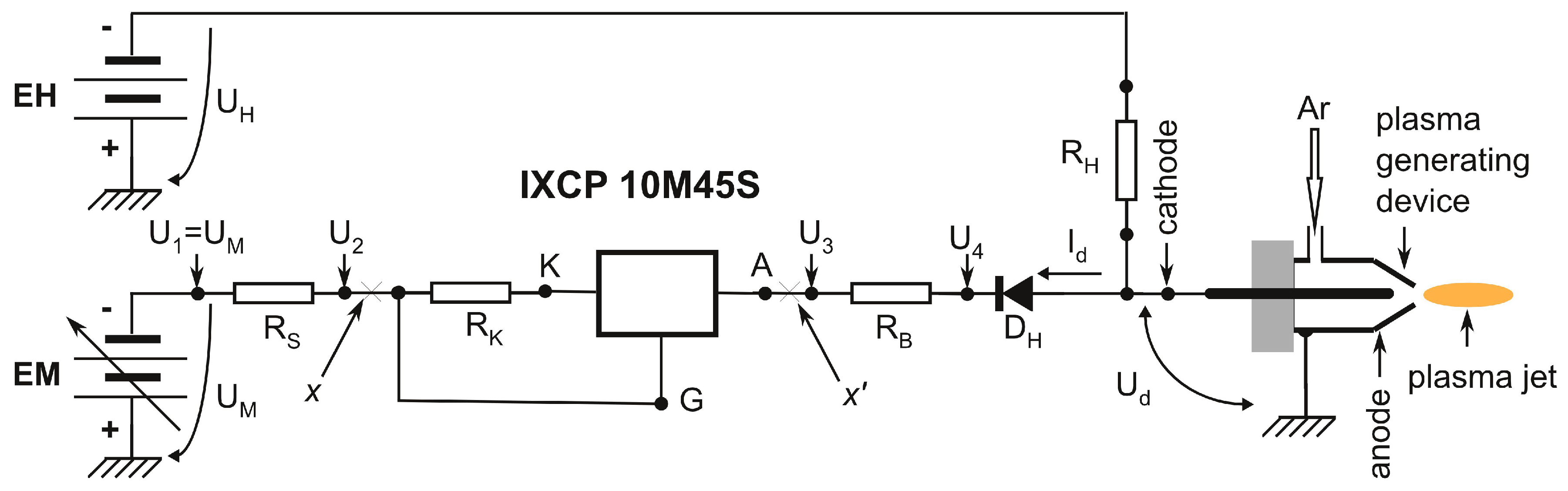
A schematic diagram of the experimental setup is shown in
Figure 1. Typically, in the case of a dc generated plasma, the voltage required to be applied to the electrodes for its ignition is much higher than the voltage necessary to sustain it [
18,
19]. To form the plasma jet, two dc negative voltage sources, respectively denoted
EH and
EM, were used. One of them,
EH, is intended to ignite the electrical discharge, whereas the second,
EM, is intended to sustain the electrical discharge. The
EH voltage source only has the role of igniting the electrical discharge. A conventional dc voltage multiplier [
20,
21] was used for this purpose. After the plasma jet is formed and becomes stable, the
EH voltage source operation can be switched off. However, to secure the re-ignition of the electrical discharge in the event of its accidental interruption, the
EH voltage source was permanently switched on, giving a fixed output dc voltage
−3.2 kV that was not changed during the experiments. Its output is connected to the cathode of the plasma generating device through a resistor
= 10 MΩ. Because the current due to the
EH voltage source (on the order of
0.32 mA) can be neglected, its contribution to the discharge current
(which is on the order of 5–50 mA) is considered as having no significance for the experiment outcomes.
The EM voltage source, giving an adjustable output dc voltage in the range from 0 to −650 V, is used to sustain the electrical discharge.
An IXYS IXCP 10M45S switchable current regulator is used as a
current source device (CSD). This device has three terminals: the anode (A), cathode (K), and gate (G), and is intended to keep constant the anode (A) to cathode (K) current in the range 2–100 mA as a function of the voltage applied between the gate (G) and cathode (K) terminals [
22]. The anode–cathode current can be programmed by means of an external negative dc voltage
applied between the cathode and the gate terminals.
To afford the control voltage
, a single section of the integrated circuit (Avago Technologies ASSR-V621 type [
23]) is used, which is a dual channel photovoltaic MOSFET driver able to generate 7 V at the output terminals (open circuit state) for input current
= 10 mA. Its input and output circuits are galvanically isolated and the output voltage is determined by the input current
.
The EM voltage source output is connected to the cathode of the plasma-generating device through a circuit consisting of resistor RS, CSD, resistor RB, and diode DH, all of which are series-connected. This voltage source provides the most important contribution to the discharge current and represents the main supply voltage.
To monitor the operating parameters of the electrical circuit and implicitly of the plasma source, four voltages
and
were measured at different points of the main supply circuit, as shown in
Figure 1.
The resistor
= 1 kΩ acts as a current sensor. The discharge current is calculated as
. To immediately observe the discharge current
, a battery powered digital voltmeter (not shown in
Figure 1 and
Figure 8) was connected across the resistor
RS, its indication expressed in volts being numerically equal to the discharge current
expressed in milliamps. Next,
= 10 kΩ acts as a ballast resistor; its presence is necessary in order to obtain a stable discharge for the range of variation of the discharge current taken into consideration. According to the Kaufmann criterion [
24,
25], in order to obtain a stable discharge, the following condition must be met:
. In the actual case considered here,
. This resistor also protects the CSD so that the voltage drop across the cathode–anode terminals does not exceed the rated value under the given experimental conditions. A higher value of ballast resistance improves discharge stability and the CSD safety, but reduces the discharge current and the range in which it can vary. The total ballast resistance
was set at the design stage of the experiment to meet both constraints. Subsequent measurements certified that this was an appropriate value. The diode D
H (BY6–type) is inserted to block the current supplied by the voltage source
EH from flowing through electrical circuit of the voltage source
EM. Its forward voltage (<6 V/1 A [
26]) is negligible compared to the discharge voltage
(>100 V) as a consequence
.
Note that the CSD is not included in any additional feedback loop, acting only as a basic current regulator in its simplest form.
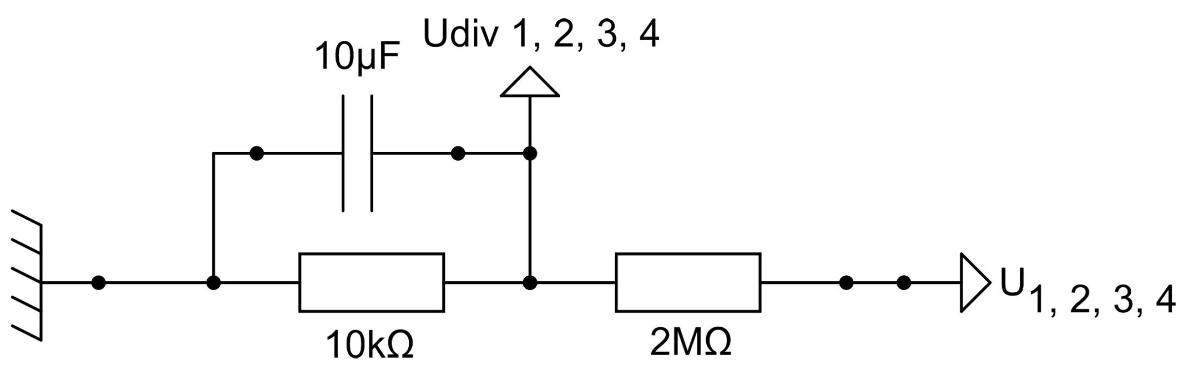
The four voltages
and
were measured using voltage dividers, each of them as shown in
Figure 2. Due to spread of the resistor values around the nominal values indicated by the manufacturer, they were calibrated previously by applying a voltage of −500 V to their inputs and measuring the resulting voltage at the output. Outputs of the voltage dividers are connected to the inputs of a data acquisition board, which performs A/D conversion and sends the results to a personal computer for recording.
Figure 2.
Schematic diagram of the voltage dividers.
Figure 2.
Schematic diagram of the voltage dividers.
Due to the specific nature of the electrical discharges, the measured voltages show fluctuation. For this reason, the plotted or tabulated data represent time-averaged values over 100 samples, with the time step between two successive samples being ≈600 ms.
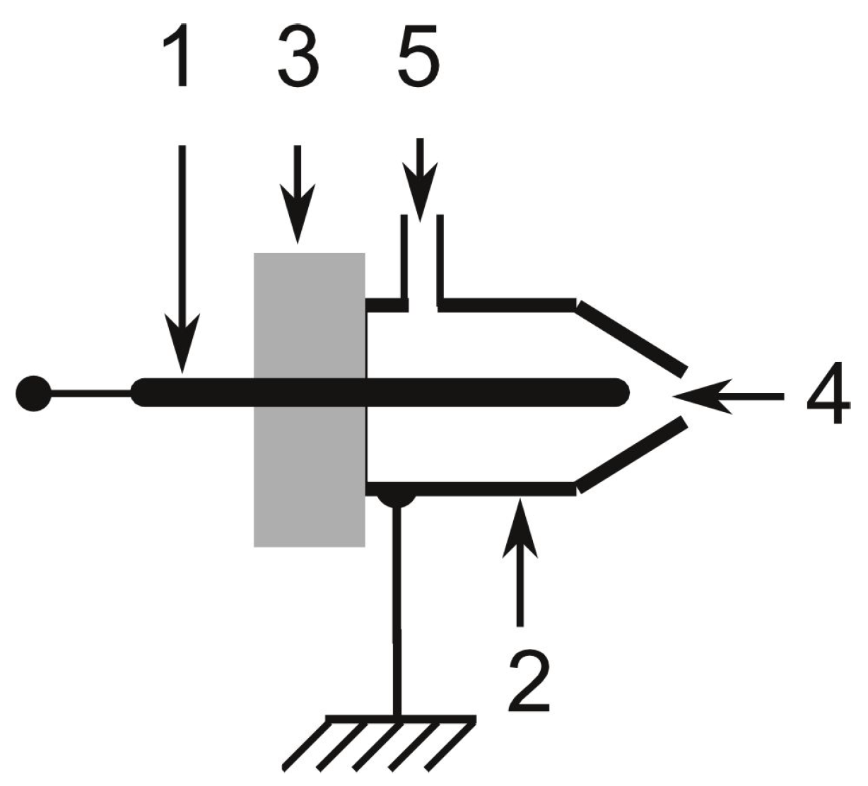
The axial section of the plasma-generating device is shown in
Figure 3. The geometry is similar to that described in [
27], consisting of an aluminum cylinder with a hollow cylindrical cavity 8 mm in diameter terminated at one end, with a conical ejector having a circular hole output 3 mm in diameter that serves to form and expel the plasma jet. This acts as an anode connected to ground. The cathode is formed by a thin metal bar 3 mm in diameter which slides along the longitudinal axis of the cylindrical cavity, its position being adjusted manually so as to obtain a specific optimal operating point that forms a stable plasma jet of maximum length. The working gas consists of Ar supplied through a lateral hole oriented perpendicular to the cylindrical cavity longitudinal axis. The gas is maintained at a constant flow rate by means of a gas flow controller (Alicat Scientific MC-20SLPM).
Figure 3.
Axial section of the plasma generating device cavity (not to scale): 1—cathode; 2—anode; 3—high voltage insulator; 4—output hole; 5—working gas input.
Figure 3.
Axial section of the plasma generating device cavity (not to scale): 1—cathode; 2—anode; 3—high voltage insulator; 4—output hole; 5—working gas input.
3. Results
To assess the effect of the CSD, a series of measurements without the CSD was performed. For this purpose, the CSD was removed and replaced by a conductive wire connecting points
x and
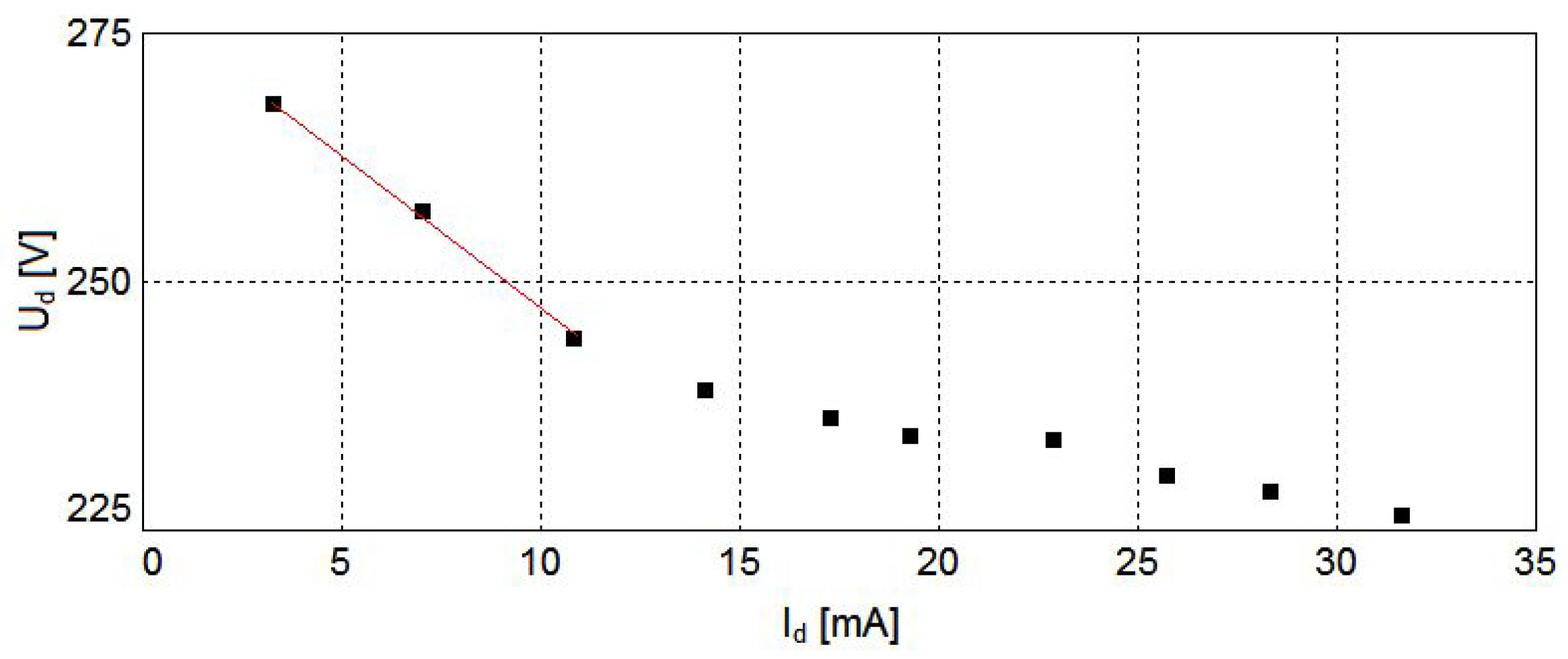
of the circuit. The current–voltage characteristic of the discharge for a series of experimental points within the discharge current range of interest is shown in
Figure 4.
Figure 4.
Current–voltage characteristic of the discharge. Experimental points are represented by black squares. The thin red line joining the first three experimental points was used to estimate the maximum differential resistance . The working gas consisted of Ar at a flow rate of 4 LPM.
Figure 4.
Current–voltage characteristic of the discharge. Experimental points are represented by black squares. The thin red line joining the first three experimental points was used to estimate the maximum differential resistance . The working gas consisted of Ar at a flow rate of 4 LPM.
As can be seen in
Figure 4, under the considered experimental conditions, the current–voltage characteristic exhibits negative resistance which varies as a function of the discharge current
. The maximum slope of the current–voltage characteristic appears to be in the region of the first three experimental points (joined by a thin red line). Based on this observation and taking into account the experimental values used to plot the current–voltage characteristic, it can be estimated as
3.13 kΩ. When compared with total ballast resistance
= 11 kΩ, this results satisfies the Kaufmann criterion.
Next, using the experimental setup shown in
Figure 1, we measured the discharge current
as a function of the main dc supply voltage
under the specific experimental conditions listed in
Table 1.
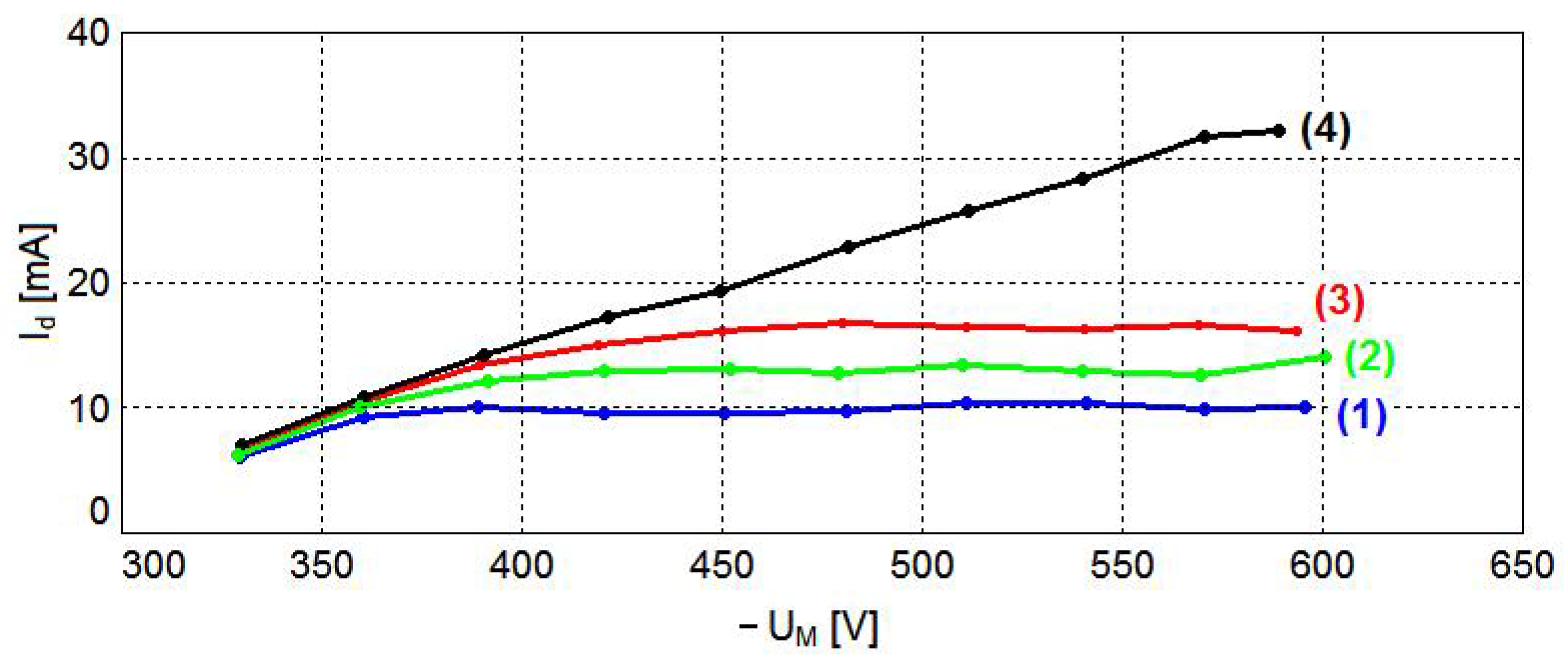
Figure 5 presents the variation of the discharge current
as a function of the main dc supply voltage
, corresponding to the four cases listed in
Table 1. The working gas consisted of Ar at a flow rate of 4 LPM.
Figure 5.
Variation of the discharge current
as a function of the main dc supply voltage
for: (1—blue)
= −2.9 V; (2—green)
= −2.7 V; (3—red )
= −2.5 V; and (4—black) without CSD. The
voltage step ≅ 30 V. The experimental setup shown in
Figure 1 was used. The working gas consisted of Ar at a flow rate of 4 LPM.
Figure 5.
Variation of the discharge current
as a function of the main dc supply voltage
for: (1—blue)
= −2.9 V; (2—green)
= −2.7 V; (3—red )
= −2.5 V; and (4—black) without CSD. The
voltage step ≅ 30 V. The experimental setup shown in
Figure 1 was used. The working gas consisted of Ar at a flow rate of 4 LPM.
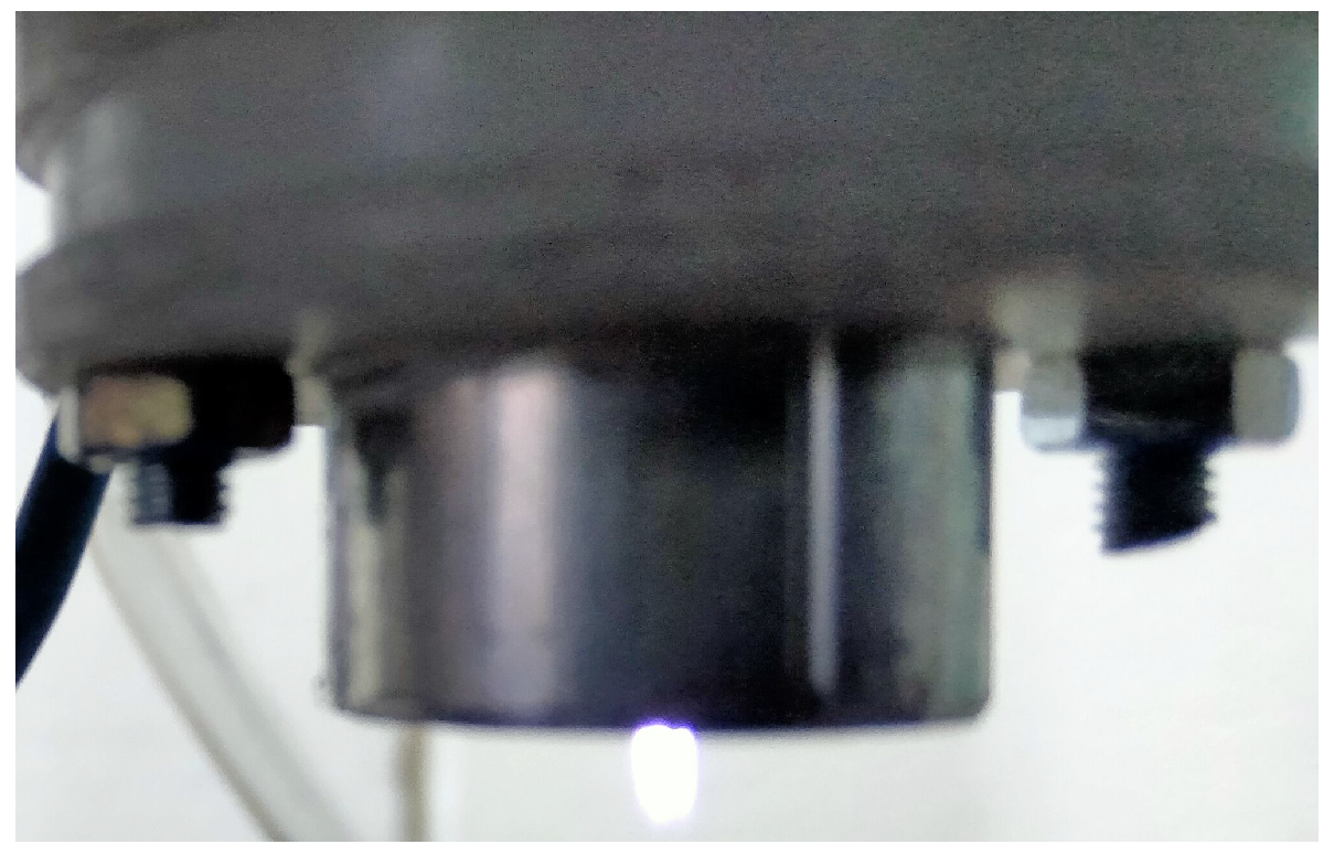
During the experiments, a stable cold (non-thermal) plasma jet with a length of about 4 mm was obtained, as shown in
Figure 6. To observe the variation of the gas temperature
T as a function of the discharge current
, a K-type thermocouple was placed about 3 mm from the plasma jet output hole. The measured values are shown in
Table 2.
Figure 6.
Image of the plasma jet. The working gas consisted of Ar at flow rate of 4 LPM.
Figure 6.
Image of the plasma jet. The working gas consisted of Ar at flow rate of 4 LPM.
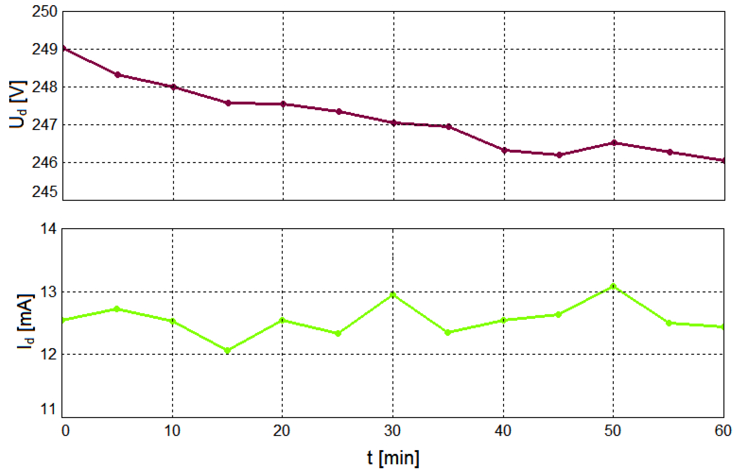
To assay the long-term course of the experimental circuit, the variation of the discharge voltage and current was monitored for 1 h. The discharge was previously ignited and maintained for 10 min in order for the CSD to reach thermal equilibrium with the ambient environment. The measurement results are shown in
Figure 7.
Figure 7.
Time variation of the discharge voltage (top) and discharge current (bottom). Time step ≅ 5 min, = −450 V, and = −2.7 V. The working gas consisted of Ar at a flow rate of 3 LPM.
Figure 7.
Time variation of the discharge voltage (top) and discharge current (bottom). Time step ≅ 5 min, = −450 V, and = −2.7 V. The working gas consisted of Ar at a flow rate of 3 LPM.
4. Discussion
The experimental results demonstrate that the topology taken into account for the electrical supply system works as expected. It is able to drive a cold plasma jet generating device while keeping the discharge current approximately constant at a programmed value. As can be seen in
Figure 5, if the main dc supply voltage magnitude |
| exceeds a threshold value |
|, then the discharge current
is roughly constant. As a result, beyond this threshold voltage, the electrical supply system operates in a current source regime. A minimum value of the main dc supply voltage magnitude is necessary to compensate for the voltage drop across ballast resistor (actually
) and discharge voltage |
|, which remains approximately constant for a given discharge current
. Therefore, this threshold voltage can be estimated as |
| =
.
Table 2 shows the average values for the discharge current
, discharge voltage
, threshold voltage |
|, and gas temperature
T when the electrical supply system operates in the current source regime. It should be taken into account that the temperature value depends on the thermocouple position relative to the plasma jet, which is tabulated for the purpose of comparing the three cases.
Table 3 lists the maximum anode–cathode
voltage, calculated as
, and dissipated power
, calculated as
, for the CSD, corresponding to the considered experimental conditions.
In the case of an IXYS IXCP 10M45S device, the maximum ratings values for the voltage between the anode (A) and cathode (K) is 450 V, whereas the maximum allowed dissipated power is 40 W [
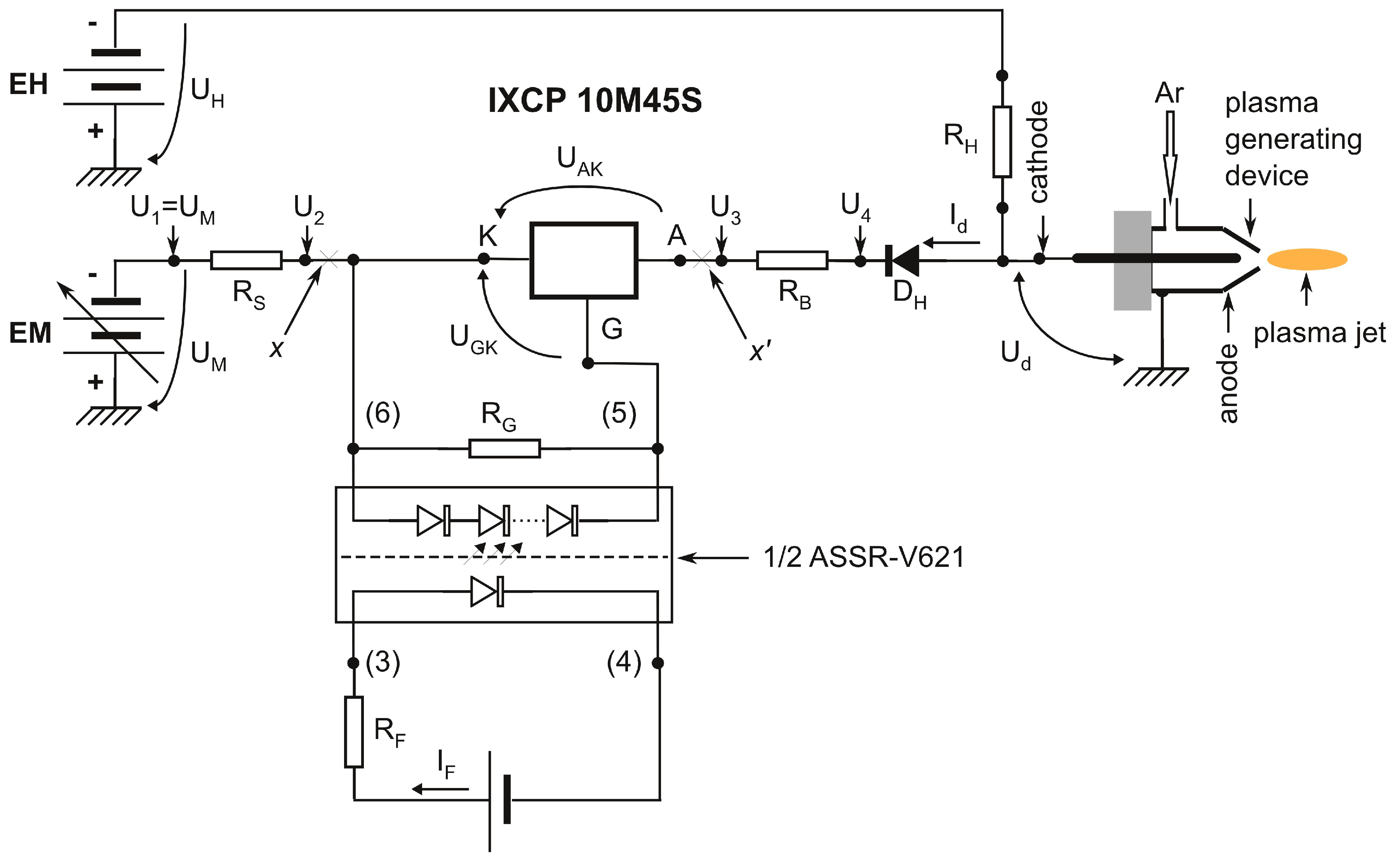
22]. To avoid overheating, the CSD was mounted on an aluminium heatsink. Therefore, by means of proper design of the electric circuit, both the discharge stability and running of the semiconductor component within the safe operational area can be achieved. This type of CSD may also operate in a current source regime using another configuration presented in
Figure 8. The anode–cathode current is programmed by means of an external resistor
connected between the cathode and gate terminals of the CSD. The datasheet indicates 10 mA as a typical value for
= 300 Ω. In fact, the same principle is used as in the case of the circuit presented in
Figure 1. The negative voltage applied between the cathode and gate terminals is due to the voltage drop across resistor
as a result of the discharge current
.
Figure 8.
Another possible configuration in which the electrical circuit operates as a current source. The anode–cathode current is controlled by the external resistor .
Figure 8.
Another possible configuration in which the electrical circuit operates as a current source. The anode–cathode current is controlled by the external resistor .
The described solution based on inserting the CSD in circuit, as shown in
Figure 1, allows for the creation of a system that generates plasma operating at a constant discharge current while being adjustable within a certain range. Although the CSD is inserted on the high-voltage side of the electrical supply circuit, the current discharge can be adjusted at any time by the user in a simple and safe manner, since the external voltage control can be applied through a circuit that is galvanically isolated. The variation of the discharge current
can be achieved in this way without changing the ballast resistance, thereby preserving the electrical discharge stability. The described system does not contain processors or other digital signal processing elements. This affords it a high degree of immunity against sources that generate EMI and better reliability. As seen in
Figure 7, under conditions where the discharge voltage
gradually decreases, the discharge current
exhibits variations with an amplitude of approximately ±0.5 mA in the long term. This variation can be considered acceptable in many applications. As mentioned above, the CSD acts as a basic current regulator without any feedback. Any variation of the chip temperature, for example, leads to variation of the anode–cathode current. Based on the fact that the discharge current
can be adjusted via the voltage
, better control of the discharge current can be obtained by including the CSD in a negative feedback loop by comparing the actual current value with a reference value. If the goal is to create a system that generates plasma while operating at a constant and predetermined discharge current that never changes, then the solution presented in
Figure 8 is more practical because of its simplicity. An issue that should be noted is that the discharge current is extremely sensitive to variation of the external voltage. Small variations of
can lead to significant variations of the discharge current
.
In conclusion, the described technical solution meets the work aim and the results represent an experimental proof-of-concept (TRL3 level).
In
Table 2, it can be seen that the bulk gas temperature
T can be controlled by means of the discharge current
and implicitly by the voltage
. The next stage of development will consider including a paired CSD/temperature sensor in a negative feedback control loop, with the aim of maintaining the gas temperature at a constant and preset value.