Abstract
The removal of defective surface layers can substantially improve the quality of various products. It can be carried out using beams of accelerated ions or fast argon atoms. However, it is difficult to process the inner surface of narrow channels. In the present work, a narrow beam of fast argon atoms is used to sputter and polish the inner surface of drawing dies with 5.7 mm wide working channels. Due to the high angle of incidence to the channel walls, sputtering with fast argon atoms decreased their roughness to Ra ~ 0.004 µm.
1. Introduction
The drawing of rods, pipes, or wire occurs during the metalworking process under the action of the tensile force of the metal, which occurs when the cross-section decreases and the length of the workpiece passing through the die increases. During the drawing process, the metal surface undergoes plastic deformation as a result of the interaction occurring at the boundary of the die and the workpiece. Therefore, the properties of the inner surface of the die largely determine its service life and the surface quality and dimensional accuracy of the products and therefore the cost and economy of the drawing process [1,2].
Currently, a popular material for making dies is tungsten carbide (often with 6% cobalt as a binder). The main causes of failure on the inner surface of tungsten carbide die holes are wear or cracks, usually caused by the surface having insufficient wear resistance. They occur in wet drawing due to corrosion leading to leaching of the cobalt binder holding the powder together and also due to workpiece adhesion caused by the high chemical affinity and friction coefficient of tungsten carbide with the workpiece material.
An effective method of reducing the incidence of such failures is to apply a suitable coating to the inner surface of the die channel. This coating must be wear-resistant and erosion-resistant and have a low coefficient of friction and low chemical affinity with the workpiece material. In recent years, various tribological or protective coatings have been used to improve wear resistance, eliminate adhesion, or enable the drawing process to be carried out without lubrication. For example, CrN and TiAlN coatings have been shown to increase the service life of tungsten carbide dies used for copper by almost three times [3].
In previous work [4], a process for the semidry/dry drawing of wire from aluminum material was implemented, improving the accuracy of the drawn wire surface and resulting in a decrease in drawing resistance as a result of the deposition of a DLC coating layer on a tungsten carbide die [5].
The Nimonic 901 superalloy is also used as a material for the manufacturing of dies. This is a highly effective alloy material with excellent high-temperature strength, oxidation resistance, corrosion resistance, and wear resistance. It is mainly composed of elements such as nickel, chromium, iron, titanium, aluminum, and cobalt, with a nickel content of up to 50%. This alloy can not only withstand high temperature but also maintain oxidation resistance and excellent mechanical properties at high temperature. It is suitable for use in the high-temperature and high-pressure corrosive environment of the production process.
The superalloy is used in a wide range of applications, including high-temperature valves, wheel shafts, turbine blades, chemical reactors, gas turbines, and other products. It is used to manufacture aircraft and gas turbine parts, such as turbine rotors, compressor disks, hubs, and shafts, with a service temperature of ~600 °C.
Metal forming and drawing involve forcing hot metal through a die to form a pressed rod, tube, or wire. During processing, the die is subjected to extremely harsh conditions, and it must maintain high hardness when hot, be strong and rigid, be resistant to thermal shock, and be chemically stable.
For copper and brass extrusion and drawing, dies are traditionally made of steel. However, steel dies provide a poor surface finish and have a short service life. To eliminate the problems with metal dies, ceramic dies were introduced.
The surface roughness of the inner channel of the die has a significant impact on the service life and productivity of the die.
When forming a blank with a die, high friction occurs between them. It can be reduced by using a lubricant, which also ensures cooling of the die and the blank. As the drawing speed increases, cooling becomes increasingly important. The optimal solution comprises solid lubricant coatings, which prevent direct contact between the die and the blank.
In industrial applications of cold drawing, the main reason for the failure of dies is wear. It affects the efficiency of the drawing process, tolerances of the formed parts, metal consumption, and the service life of the die. The wear of the die occurs locally during the drawing process.
All surfaces of the dies were polished to ensure good fluidity of the plastic material and low friction values. The surface was treated by stripping, grinding, and polishing with diamond paste. Figure 1 shows an example of a tungsten carbide drawing die installed in a clamp for drawing copper wire.
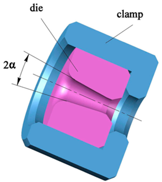
Figure 1.
Diagram of a die for drawing round wire in a clamp.
Figure 2 shows the internal contour of the die, consisting of four important zones: the input (inlet) zone (1), the working (reducing) zone (2), the calibrating zone (3), and the output zone (4).
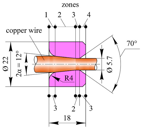
Figure 2.
Schematic of main inner zones of the die.
- The input zone is a part of the die channel that serves to facilitate the introduction of the workpiece into it and the supply of lubricant to the working area. The surface of the input zone has a roughness of no more than Ra = 0.63 µm, the angle at the cone apex is 40–50°, and its length is 1–1.5 times greater than the diameter of the calibrating zone. The input zone is designed to direct the lubricant flow into the working area of the die, where the lubricant is compacted on the surface of the workpiece during drawing.
- The working zone is the part of the die channel used to deform the workpiece, during which its cross-section is reduced to the specified value. This is the most critical part of the die channel. The surface roughness here should not exceed Ra = 0.063 µm. The angle of the working zone of the die is designated by 2α, where α is the angle between the generatrix of the working zone and the axis of the die channel. The working zone is its most important section. The efficiency of any die for drawing out a workpiece is determined by the design and quality of the surface treatment in this zone.
- The calibrating zone serves to impart the dimensions of the cross-section of the drawn blank to the specified accuracy. An overestimated length of the calibrating zone increases the drawing force, while an underestimated length leads to its rapid wear. The surface of this zone should have a mirror shine, and its roughness should not exceed Ra = 0.05 μm. The function of the calibrating zone is the final control of the diameter, flatness, and smoothness of the drawn blank. The highest normal stress occurs in the blank near the entrance to the working zone and at the beginning of the calibrating zone of the die. The surface of the die in the working and calibrating zones should be well polished to ensure good flow of the plastic material and low friction values.
- The exit zone serves to protect the drawn metal from damage when it exits the calibrating zone. Usually, the exit zone has the shape of a truncated cone with an angle at the top of 60–70°. Its length is approximately two times less than the diameter of the calibrating zone.
The possibilities for mechanically polishing the die working surface are limited. Firstly, the small dimensions of the internal space of the die working channel do not allow the introduction of the tools necessary for processing. In addition, even polishing the external surfaces of the die does not allow for reducing the roughness below Ra = 0.05 μm. Therefore, it was proposed in this study to sputter and polish the surface of the dies with a beam of fast argon atoms.
2. Materials and Methods
To study processing of the die inner surface with a beam of fast argon atoms, a set of commercially available dies was purchased (Figure 3). The wear was studied using samples of tungsten carbide drawing dies in a cobalt binder (GL 20, 88 wt.% WC and 12 wt.% Co, with a hardness of 1250 HV10, a density of 14.3 g/cm3, and an average grain size of 2.5 μm), manufactured by wire electrical discharge machining.
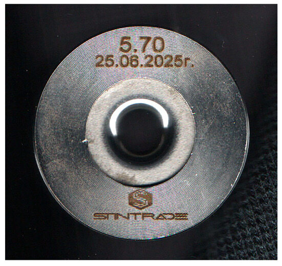
Figure 3.
Photograph of a tungsten carbide drawing die used to study the wear of the dies.
A tungsten carbide die of 18 mm long and 22 mm in diameter is embedded in a 27 mm long steel clamp, which is 43 mm in diameter (Figure 4). The length of the input zone is 3 mm, the working zone is 10 mm long, the length of the calibrating zone is 2 mm, and the output zone is 3 mm long. The calibrating zone diameter is 5.7 mm, and the angle of the die working zone is 2α = 12°.
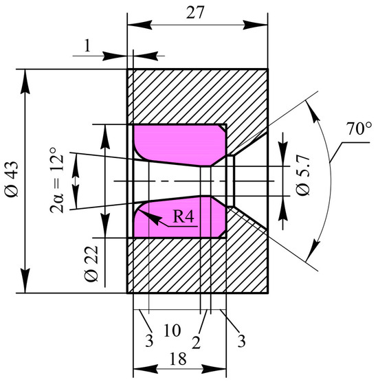
Figure 4.
Schematic of the tungsten carbide die in a steel clamp.
Before the treatment of the die with a beam, its roughness—mean arithmetic deviation of the profile (Ra)—was measured. The probe method of measuring surface roughness was used. It is a contact method, in which measurements are made using a profilometer Mitutoyo Surftest SJ-210 (Mitutoyo Corporation, Kawasaki, Japan). It is a sensitive sensor equipped with a thin, sharply sharpened diamond needle with a probing head (Figure 5).
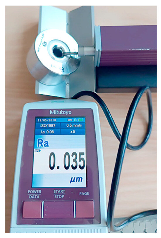
Figure 5.
Photograph of a tungsten carbide die and the Mitutoyo Surftest SJ-210 profilometer.
The diamond needle is pressed and moved parallel to the surface being examined. In places where microroughness (protrusions and depressions) occurs, mechanical vibrations of the measuring head of the needle occur. These vibrations are transmitted to the sensor, which converts the mechanical energy of the vibration into an electrical signal, which is amplified by the converter and measured. The recorded parameters of this signal exactly repeat the irregularities on the rough surface of the product.
The probing head of the Mitutoyo Surftest SJ-210 profilometer is smaller than the inner diameter of the die, which allowed us to introduce the probe into the working zone and measure the roughness of the inner walls of the die.
The average roughness in each zone of the die was obtained by averaging all the values obtained. The measurement results for two identical dies show that the average roughness of the first and second dies are, respectively, equal to 0.042 and 0.047 µm in the input zone, 0.051 and 0.052 µm in the compression zone, and 0.045 and 0.043 µm in the calibration zone. It means that the initial parameters of the purchased dies are very close.
Some dispersion of the measured parameters can be explained by the presence of surface defects. One of the ways to rectify the defects is to remove the defective surface layer. For the removal of the defective surface layer, sputtering with fast argon atoms was used.
Figure 6 shows a diagram of the setup for sputtering and polishing the working surface of a ceramic die with a beam of fast atoms. It contains a 40 cm long vacuum chamber with an inner diameter of 30 cm, which is hermetically connected to the beam source. The working gas is argon, and it is continuously fed into the hollow cathode of the beam source. Through the cathode and the grid, it enters the chamber and is pumped out of it by a turbomolecular pump TMP-V1704LM (Shimadzu Corporation, Kyoto, Japan). The argon pressure is regulated by a gas feed device.
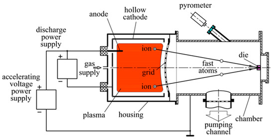
Figure 6.
Scheme of the die processing with a beam of fast argon atoms.
When a discharge voltage of Ud = 200–400 V is applied between the hollow cathode and the anode installed inside it at an argon pressure of 0.5 Pa, a hollow cathode glow discharge is ignited. When an accelerating voltage of U = 1–3 kV is applied between the anode and the chamber, the ions are accelerated in the space charge layer between the plasma and the grid and fly through its openings with an energy of eU.
Focusing a beam of fast neutral atoms is impossible. A concave accelerating grid was used to generate an intense beam of fast argon atoms with a cross-sectional diameter of 5 mm. Accelerated ions begin moving from the grid toward its focus and, due to charge exchange collisions, are converted into fast neutral atoms along the way. The generation of a beam capable of entering a die with a working channel diameter of 5 mm owing to charge exchange on the solid target is impossible.
After passing through the grid, the accelerated ions collide with argon atoms and, as a result of charge exchange, are transformed into fast neutral atoms. At a pressure of p = 1 Pa, the density of argon atoms can be considered equal to no = 2.5 × 10²⁰ m−3 [6]. The charge exchange cross-section of argon ions with an energy of eU = 3 keV is equal to σc = 0.2 × 10⁻¹⁹ m2 [7,8], and the charge exchange length of ions is λc = 1/noσc = 0.2 m, which is two times shorter than the distance of 40 cm between the grid and its focal point. Therefore, it can be considered that all ions that have passed through the grid arrive at the surface of the die, mounted on the holder near its focal point, in the form of a converging flow of fast neutral argon atoms.
The velocity v (m/s) of substrate sputtering is as follows:
where Y is the sputtering coefficient, equal to the ratio of the number of atoms leaving the substrate to the number of ions bombarding its surface, j is the ion current density on the substrate, e is the elementary charge, M is the mass of an atom of the substrate substance, and ρ is its density.
v = Y(j/e) (M/ρ),
The rate of the substrate material removal by fast atoms depends on their energy ε and the angle β of incidence on its surface. At β = 0, the sputtering coefficient, equal to the ratio of the number of knocked-out atoms to the number of fast argon atoms knocking them out, can be estimated using the Smith formula [9]:
where Z1 (18) and Z2 (74) are the charge numbers of the nuclei of the ion (argon) and the atom of the sputtered substance (tungsten), M1 (40) and M2 (183.8) are their mass numbers, and the heat of sublimation of the sputtered substance εo is expressed in electron volts and is equal to εo = 8.76 eV for tungsten. At an argon ion energy of ε = 3 keV, the Smith formula gives the value Y = 0.545 for the sputtering coefficient of the tungsten alloy. When sputtering a tungsten substrate with ρ = 14.3 × 10³ kg/m3 and M = 183.8 × 1.66 × 10−27 kg = 30.51 × 10⁻²⁶ kg with argon ions with an energy of 3 keV, the sputtering yield Y ≈ 0.545, and at a current density j = 100 A/m2, the sputtering rate v = 0.545 × (100/1.6 × 10−19)(30.51 × 10⁻²⁶/14.3 × 103) = 26.2 μm/h.
Y = (20/εo)(Z1Z2)2(M1/M2) ε/(ε + 50 Z1Z2)2
In a large hollow cathode with a diameter of 28 cm and a length of 30 cm, the discharge plasma is distributed quite uniformly [10]. Therefore, the ions’ current density in the grid circuit is approximately equal to their current density on the cathode. The accelerating grid with a diameter of 24 cm (Figure 6) extracts ions from the plasma limited by the grid with a surface area of Sg = π122 = 450 cm2 and a hollow cathode with a surface area of Sc = π28 × 40 + 2π142 = 4748 cm2.
The total surface area of the ion-emitting plasma is S = Sg + Sc = 450 + 4748 ≈ 5200 cm2, and at a discharge current of I = 5.2 A, the current in the hollow cathode circuit of ions accelerated in the cathode layer of the discharge to ~300 eV is Ic = 4.75 A, and the current in the grid circuit of ions accelerated to an energy of eU = 3 keV is Ig = 0.45 A. At the grid transparency η = 0.75, a noticeable proportion (25%) of high-energy ions are absorbed by the grid, and the rest (75%) fly through its holes and have already been converted into fast neutral argon atoms at a distance of 10–20 cm from the grid. The current of fast atoms near a grid with a surface of Sg = 450 cm2 is 0.45 A × 0.75 = 0.3375 A, and the current density increases to 0.3375/0.28 = 1.20 A/cm2 with an increase in the distance from the grid to 40 cm and a decrease in the beam cross-section from Sg = 450 cm2 to 0.28 cm2.
Accelerated particles emitted by the concave surface of the grid are concentrated near its focal point in the form of a focused beam of fast neutral argon atoms. Flat targets made of 0.5 mm thick titanium sheets were placed one after another between the grid and its focal point and irradiated with the beam. Figure 7 shows the dependence of the beam imprint diameter D on the distance d between the target and the grid. At a distance d = 40 cm, the beam imprint diameter is ~0.6 cm, and when a die with a working channel diameter of 5.7 mm is installed here parallel to the beam axis, its walls are sputtered by fast atoms with a large angle of incidence, β > 80°, onto the walls.
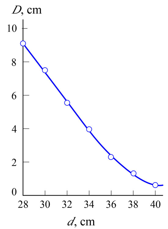
Figure 7.
Dependence of the beam imprint diameter D on the distance d between the target and the grid.
In [11], it is shown that the roughness of the substrate after treatment with a beam of fast argon atoms decreases and depends on the angle of their incidence β on its surface. If the angle does not exceed the threshold value βo ~ 50°, the rate of roughness reduction weakly depends on the angle β. When sputtering the walls of the inner channel of a die with a diameter of 5.7 mm and a length of 16 mm, the angle of incidence of atoms flying to it 40 cm from the grid with a diameter of 12 cm exceeds 70°. This should ensure an increased rate and quality of polishing of the inner channel of the die. However, to verify this, it is necessary to measure the roughness of the walls of the die channel.
The roughness of the inner surface of the die after treatment with the beam of fast argon atoms was measured using a high-precision Dektak XT profilometer manufactured by Bruker Nano, Inc. (Billerica, MA, USA). When preparing samples for measuring the roughness of the inner walls of the die, they were removed from the chamber and cut along the axis using a wire electrical discharge machine.
All samples cut from the dies were cleaned in an ultrasonic bath and dried in a hot air flow, and the roughness was measured. In the working zone, the roughness was Ra = 0.051 μm, and in the calibrating zone, it was Ra = 0.046 μm.
On the removable flange of the chamber (Figure 6), there are 3 blind holes with M6 thread and a depth of 7 mm, located evenly around a circle of ø 76 mm. Three “stud 1” parts are screwed into these blind holes.
There are two disks with a thickness of 10 mm and a diameter of 95 mm, differing in the number of holes with a diameter of 76 mm. Disk 1 has 6 holes ø 6.2 mm, and Disk 2 has 3 holes. Both disks have recesses ø 43.2 mm and are 5 mm deep in order to fit the clamp around the die (its outer diameter is 43 mm).
Disk 1 is secured to three “stud 1” parts using three M6 nuts. Three 60 mm long studs, with M6 threads, are secured to the three free ø 6.2 mm holes of Disk 1 using six M6 nuts (Figure 8a).
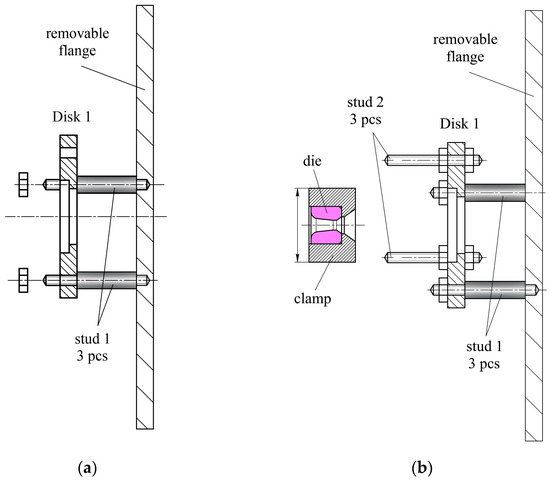
Figure 8.
Fastening on the removable flange of the chamber for Disk 1 (a) needed to mount the clamp with the die on the holder (b).
Then, three 60 mm long studs 2 with M6 threads, are attached to the three free ø 6.2 mm holes of disk 1 using six M6 nuts (Figure 8b). The holder with the die is inserted into the ø 43.2 mm recess of Disk 1 and pressed with Disk 2 by tightening three M6 nuts onto the studs. The resulting holder of the die, presented in Figure 9, was secured using screws, the chamber flange was closed, and the chamber was evacuated to 0.001 Pa.
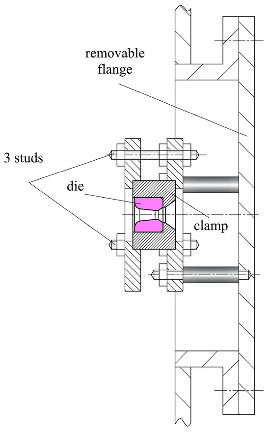
Figure 9.
Holder of the die in the clamp fastened to the removable flange of the chamber.
After feeding argon into the chamber and increasing the pressure to p = 0.05 Pa, the power sources were turned on and a hollow cathode discharge was ignited with a current of 5.2 A at a voltage of 300 V between the anode and the cathode and at a voltage of 3000 V between the anode and the chamber.
The current in the cathode circuit was Ic = 4.75 A, and the current in the grid circuit was Ig = 0.45 A. In this case, 75% of the ions with an energy of 3000 eV flew into the chamber, were recharged in it, and formed a flow of fast argon atoms with an energy of 3000 eV and a current of 0.3375 A, converging on the processed die.
After processing the die for half an hour in the specified mode, it was removed from the chamber and cut along the axis using the wire electrical discharge machining. This allowed us to measure the roughness Ra = 0.037 μm in the calibrating zone using the Dektak XT profilometer. The surface of the calibrating zone had a mirror shine after polishing.
Increasing the processing time of the second, third, fourth, and fifth dies to 1.5, 2, 2.5, and 3 h made it possible to reduce the roughness of the die calibrating zone to record low values of Ra: 0.017, 0.011, 0.006, and 0.0043 μm. The roughness measurement results are presented in Figure 10.
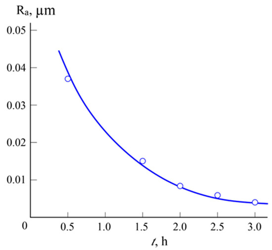
Figure 10.
Roughness of the die calibrating zone Ra versus the time t of polishing it with a beam.
To find out how polishing the inner surfaces of a drawing die influences its abrasion resistance, a homemade arrangement was used. A copper wire with a diameter of 6 mm, which is slightly larger than the die opening, was pulled through the die with force and made a reciprocating motion with a frequency of 2 Hz and a stroke of 50 mm. Every 3 min, the aperture diameter da was measured using a spinneret inspection video measuring microscope NVMII-4030Di (NORGAU, Moscow, Russia). It allowed us to obtain dependencies of the aperture diameter increment Δda on the drawing time t. Figure 11 shows that Δda increases moderately until the drawing time t exceeds the critical value to. At t ˃ to, the aperture diameter increase accelerates sharply. This is due to an increase in the drawing resistance of the surface, which hinders further drawing.

Figure 11.
Dependence of the increment of the aperture diameter Δda on the drawing time t of dies polished by a beam of fast atoms at a surface roughness of Ra = 0.0043 μm (1), 0.006 µm (2), 0.011 µm (3), and 0.017 µm (4).
The dependencies presented in Figure 11 show that with an increase in processing time and a decrease in surface roughness, the abrasive resistance improves.
The proposed method of processing the inner surface of a die with a beam of fast argon atoms can be recommended for any other difficult-to-machine parts in order to in-crease abrasive resistance and extend service life.
3. Conclusions
- The obtained results demonstrate the possibility of polishing the inner surface of the die with a beam of fast argon atoms.
- Removal by fast atoms of surface defects in the form of scratches, which are inevitable during mechanical polishing using fine abrasive powder, made it possible to reduce the roughness of the die working surface to a minimum value of Ra ~ 0.004 µm.
- Reducing the roughness of the die working surface leads to a significant increase in its abrasive resistance and service life.
Author Contributions
Conceptualization, A.S.M., M.A.V. and S.N.G.; methodology, A.S.M. and M.A.V.; software, E.S.M.; validation, A.S.M., M.A.V. and Y.A.M.; formal analysis, Y.A.M.; investigation, E.S.M. and Y.A.M.; resources, E.S.M. and Y.A.M.; data curation, M.A.V. and Y.A.M.; writing—original draft preparation, A.S.M. and M.A.V.; writing—review and editing, A.S.M. and S.N.G.; visualization, E.S.M.; supervision, A.S.M. and S.N.G.; project administration, M.A.V.; funding acquisition, A.S.M. All authors have read and agreed to the published version of the manuscript.
Funding
This research was funded by the Russian Science Foundation, grant no. 23-19-00517 dated 15 May 2023.
Institutional Review Board Statement
Not applicable.
Informed Consent Statement
Not applicable.
Data Availability Statement
The data presented in this study are available on request from the corresponding author.
Acknowledgments
The study was carried out with the equipment of the center of collective use of MSUT “STANKIN”.
Conflicts of Interest
The authors declare no conflicts of interest.
References
- Pops, H. Nonferrous Wire Handbook, Vol. 3: Principles and Practice; Wire Association International Inc.: Guilford, Australia, 1995; 678p. [Google Scholar]
- Tassi, O.J. Nonferrous Wire Handbook, Vol. 2: Bare Wire Processing; Wire Association International Inc.: Guilford, Australia, 1981; 405p. [Google Scholar]
- Navinšek, B.; Panjan, P.; Milošev, I. Industrial applications of CrN (PVD) coatings, deposited at high and low temperatures. Surf. Coat. Technol. 1997, 97, 182–191. [Google Scholar] [CrossRef]
- Murakawa, M.; Jin, M.; Hayashi, M. Study on semidry/dry wire drawing using DLC coated dies. Surf. Coat. Technol. 2004, 177–178, 631–637. [Google Scholar] [CrossRef]
- Kim, T.H.; Kim, B.M.; Choi, J.C. Prediction of die wear in the wire-drawing process. J. Mater. Process. Technol. 1997, 65, 11–17. [Google Scholar] [CrossRef]
- McDaniel, E.W. Collision Phenomena in Ionized Gases; Willey: New York, NY, USA, 1964; 775p, Available online: https://scholar.google.com/scholar_lookup?title=Collision+Phenomena+in+Ionized+Gases&author=McDaniel,+E.W.&publication_year=1964 (accessed on 25 August 2025).
- Phelps, A.V. Cross sections and swarm coefficients for nitrogen ions and neutrals in N2 and argon ions and neutrals in Ar for energies from 0.1 eV to 10 keV. J. Phys. Chem. Ref. Data 1991, 20, 557–573. [Google Scholar] [CrossRef]
- Phelps, A.V.; Greene, C.H.; Burke, J.P. Collision cross sections for argon atoms with argon atoms for energies from 0.01 eV to 10 keV. J. Phys. B At. Mol. Opt. Phys. 2000, 33, 2965–2981. [Google Scholar] [CrossRef]
- Smith, D.L. Physical sputtering model for fusion reactor first-wall materials. J. Nucl. Math. 1978, 75, 20–31. [Google Scholar] [CrossRef]
- Metel, A.S.; Grigoriev, S.N.; Melnik, Y.A.; Panin, V.V. Filling the vacuum chamber of a technological system with homogeneous plasma using a stationary glow discharge. Plasma Phys. Rep. 2009, 35, 1058–1067. [Google Scholar] [CrossRef]
- Grigoriev, S.N.; Metel, A.S.; Volosova, M.A.; Mustafaev, E.S.; Melnik, Y.A. Polishing Ceramic Samples with Fast Argon Atoms at Different Angles of Their Incidence on the Sample Surface. Plasma 2024, 7, 816–825. [Google Scholar] [CrossRef]


Disclaimer/Publisher’s Note: The statements, opinions and data contained in all publications are solely those of the individual author(s) and contributor(s) and not of MDPI and/or the editor(s). MDPI and/or the editor(s) disclaim responsibility for any injury to people or property resulting from any ideas, methods, instructions or products referred to in the content. |
© 2025 by the authors. Licensee MDPI, Basel, Switzerland. This article is an open access article distributed under the terms and conditions of the Creative Commons Attribution (CC BY) license (https://creativecommons.org/licenses/by/4.0/).