Properties of Bilayer Zr- and Sm-Oxide Gate Dielectric on 4H-SiC Substrate Under Varying Nitrogen and Oxygen Concentrations

 ,
,  , , and
Abstract
1. Introduction
2. Methodology
3. Results and Discussion
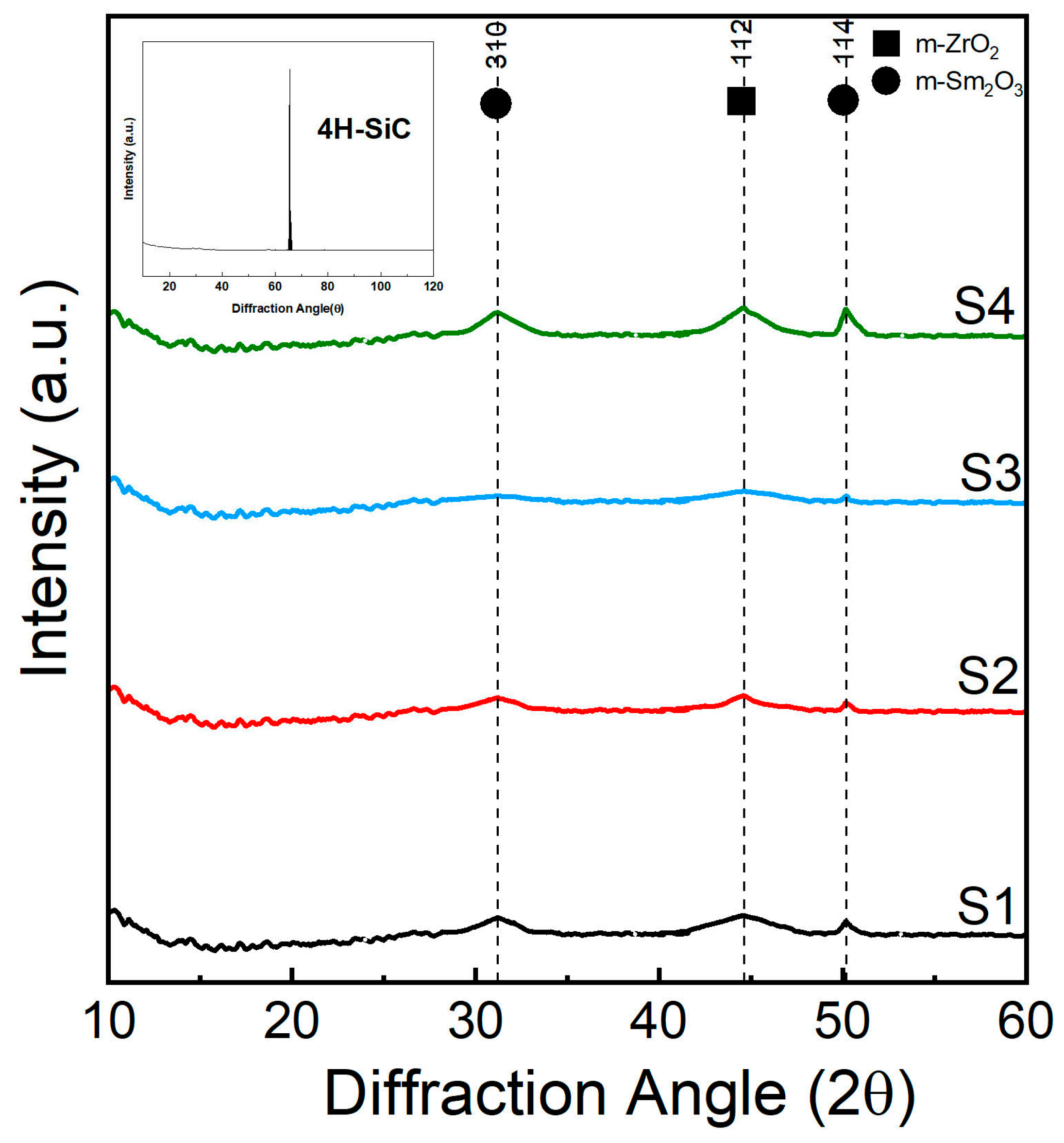
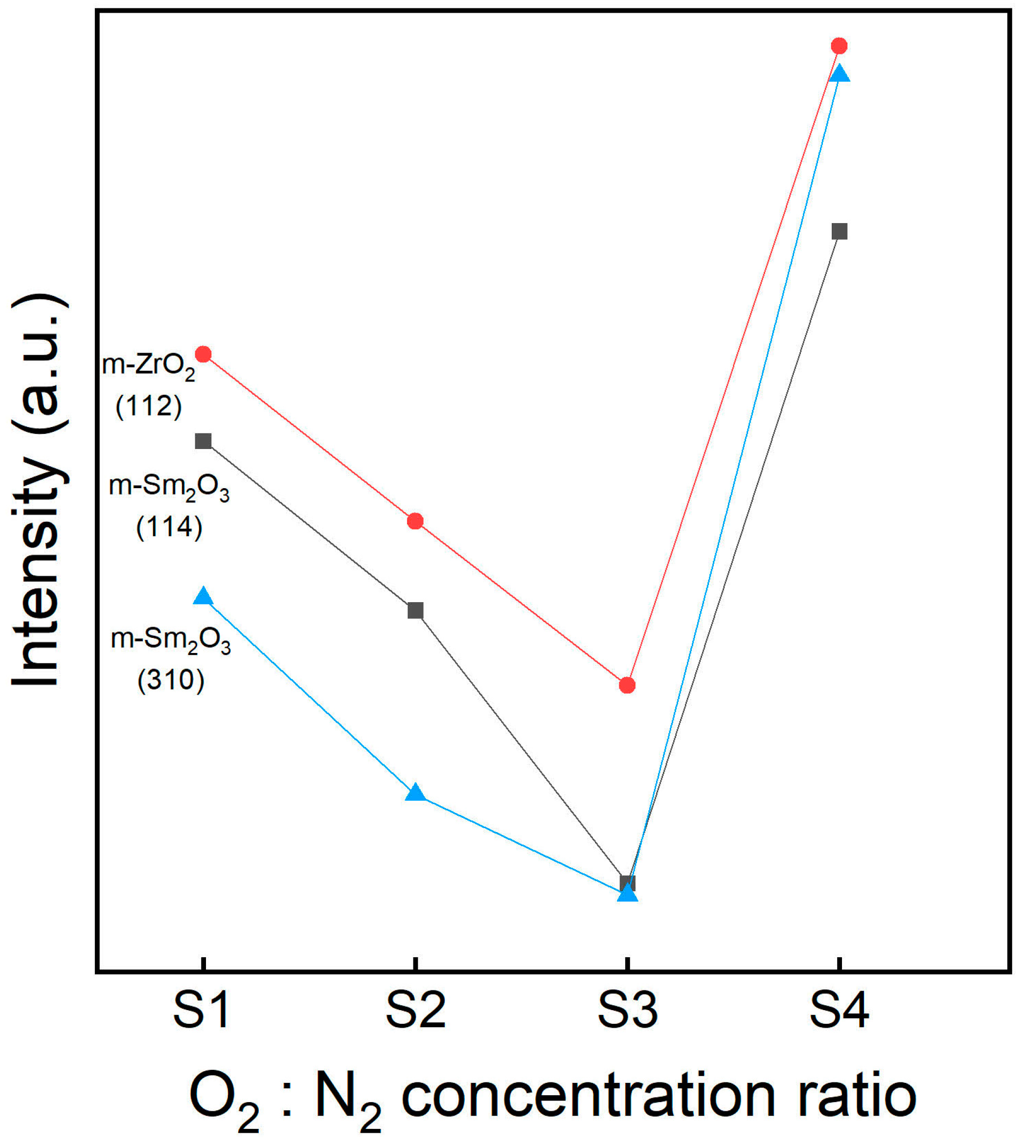
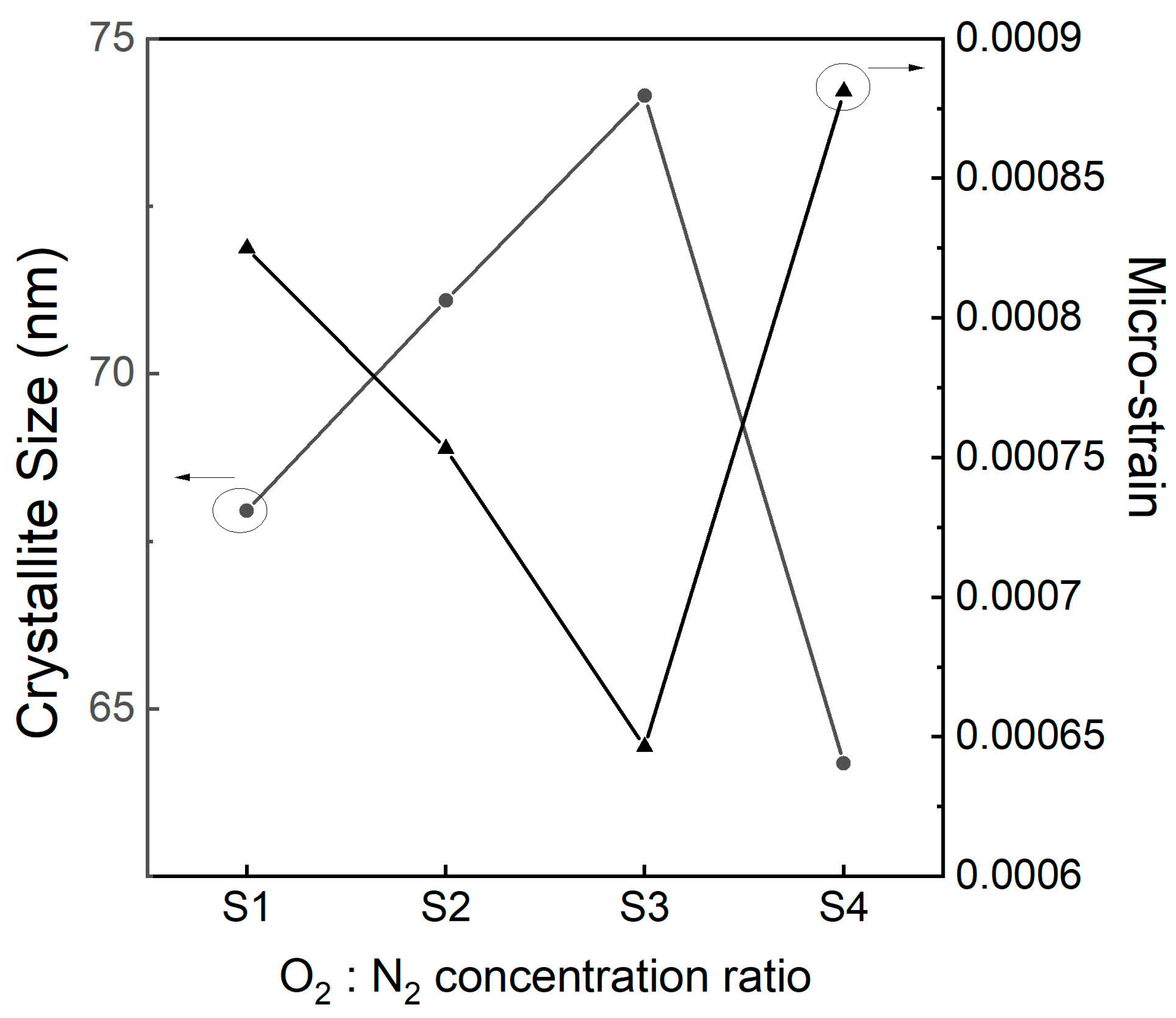
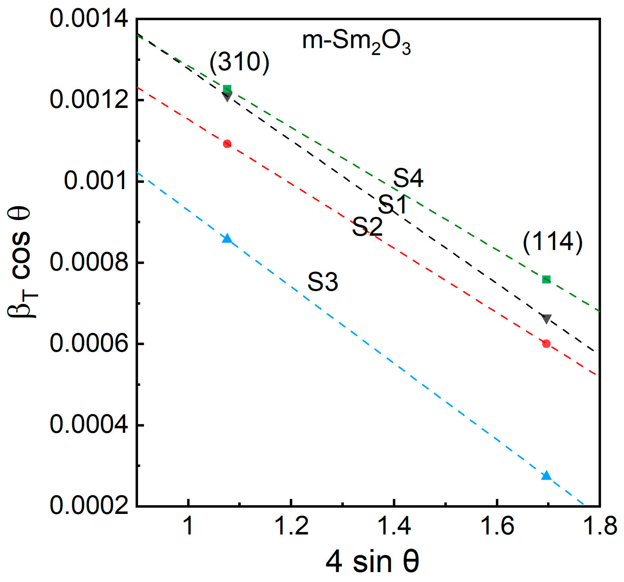
3.1. XRD Analysis
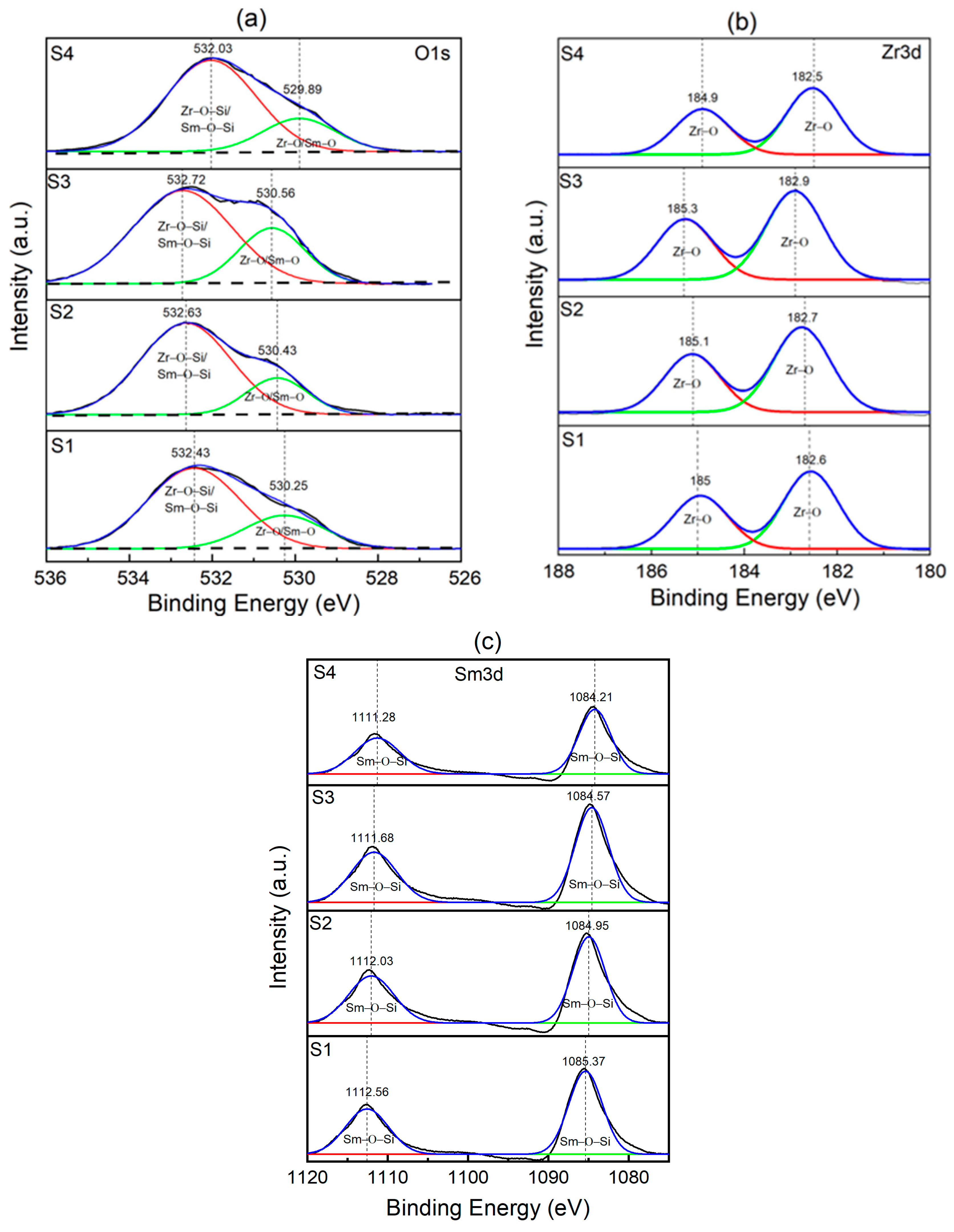
3.2. XPS Analysis
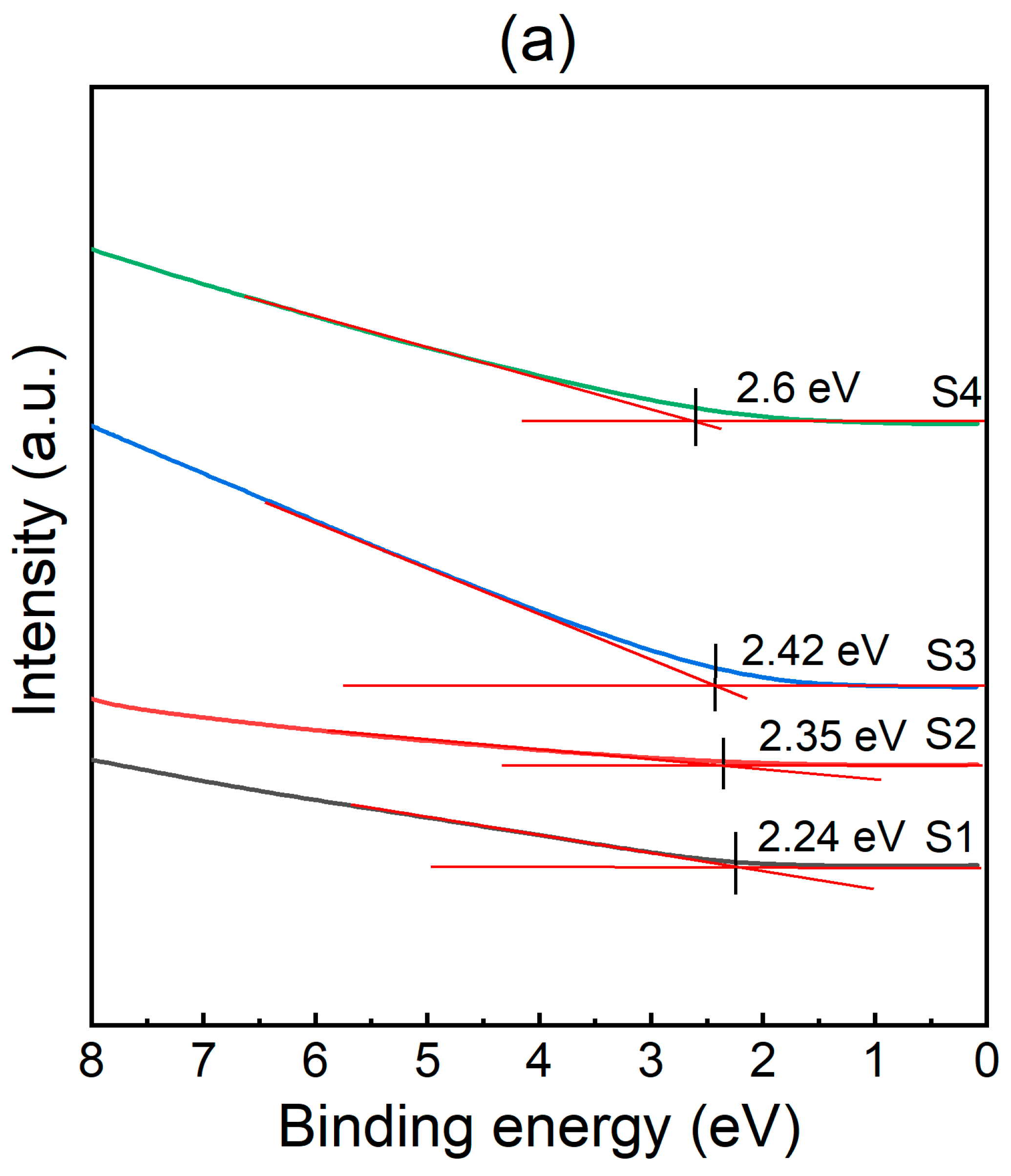
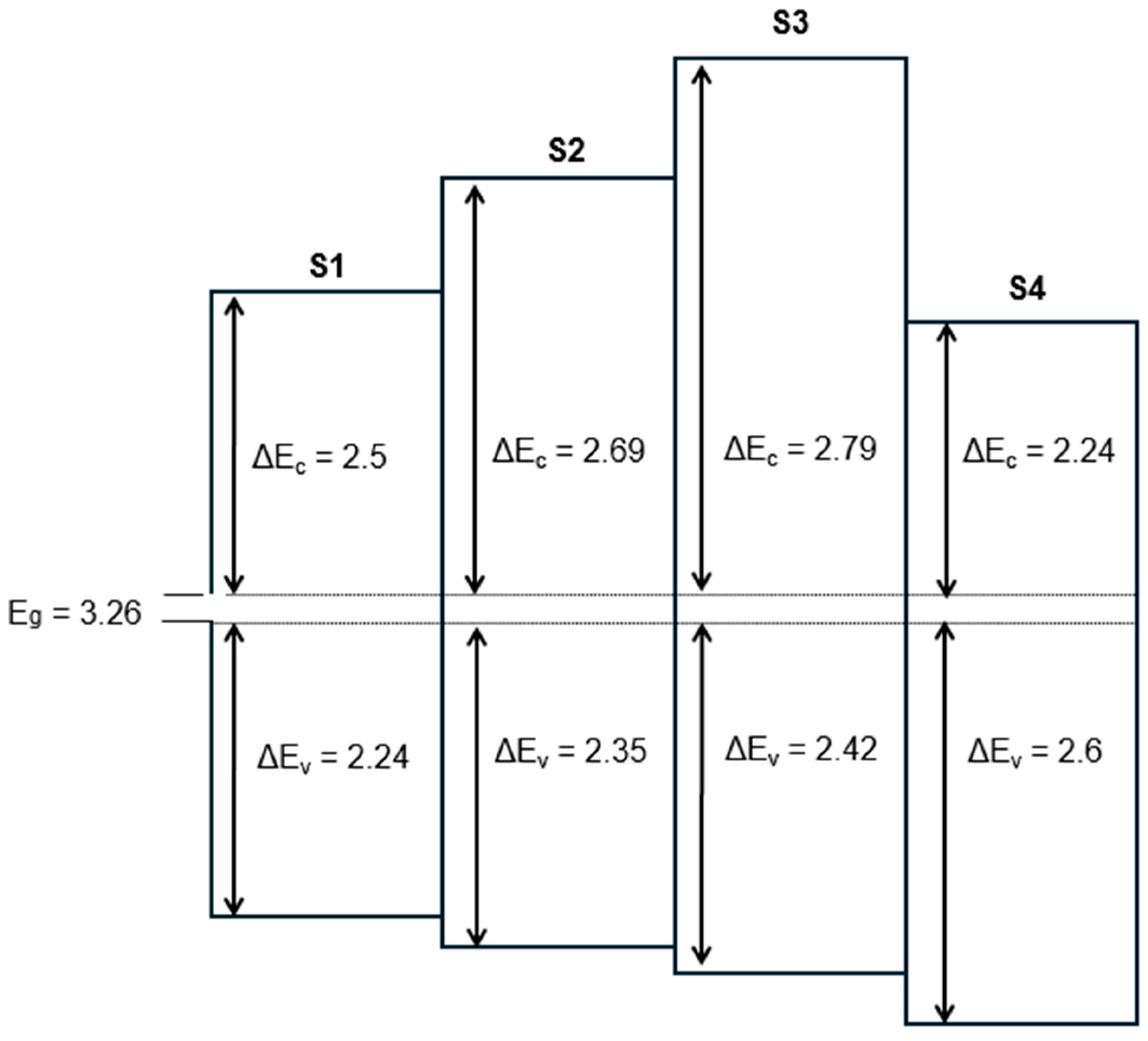
3.3. Band Alignment
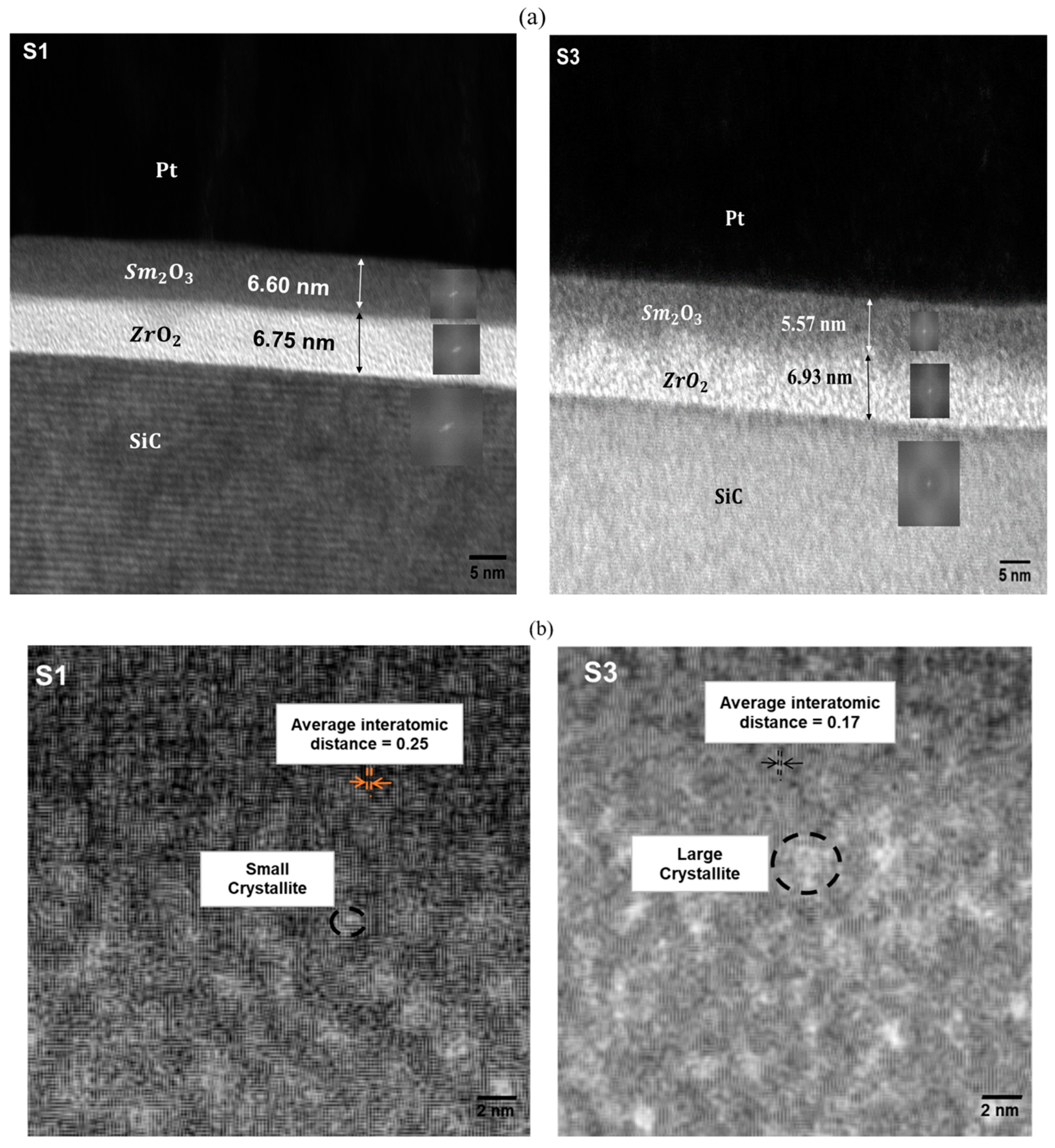
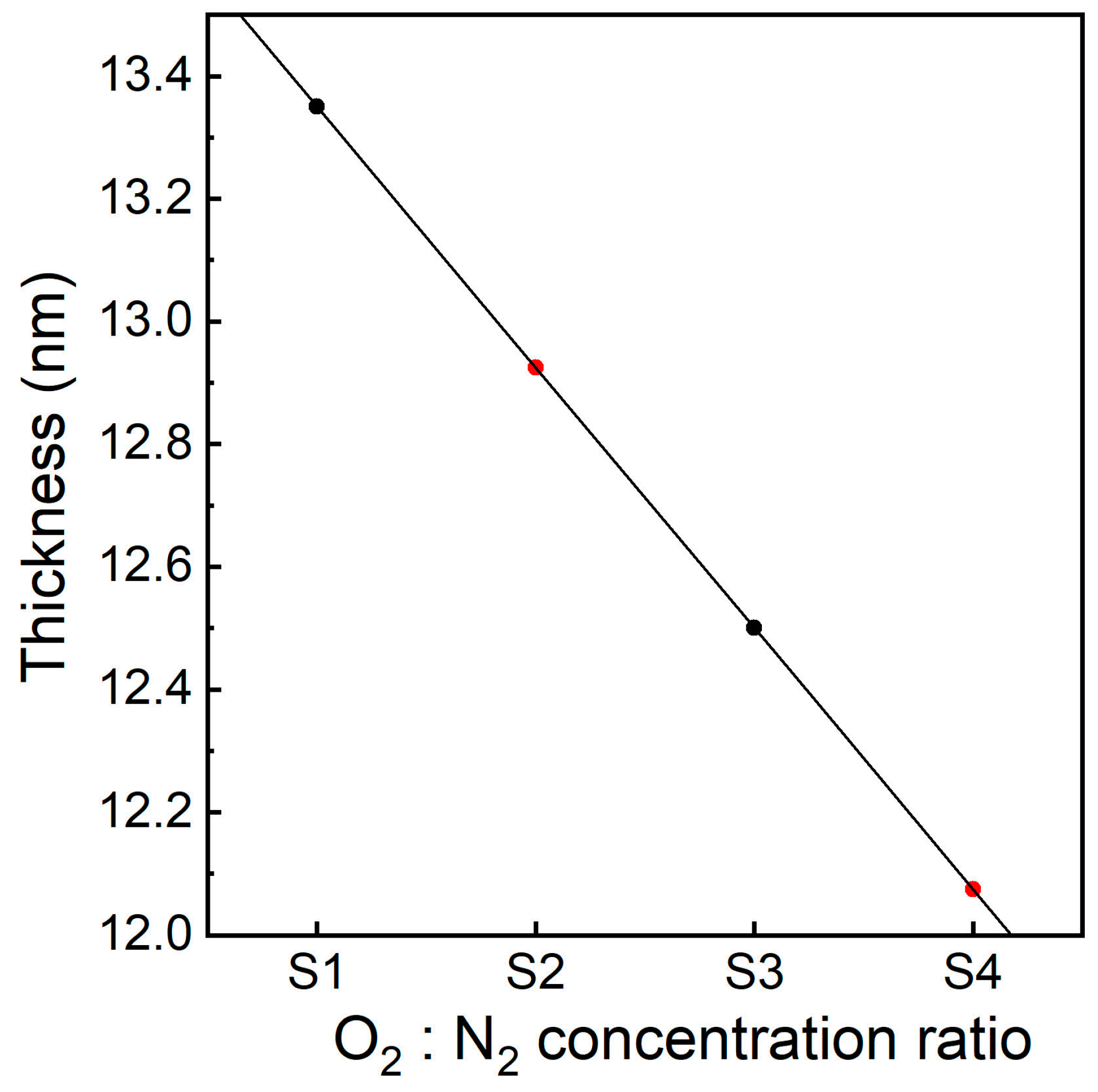
3.4. HRTEM Analysis
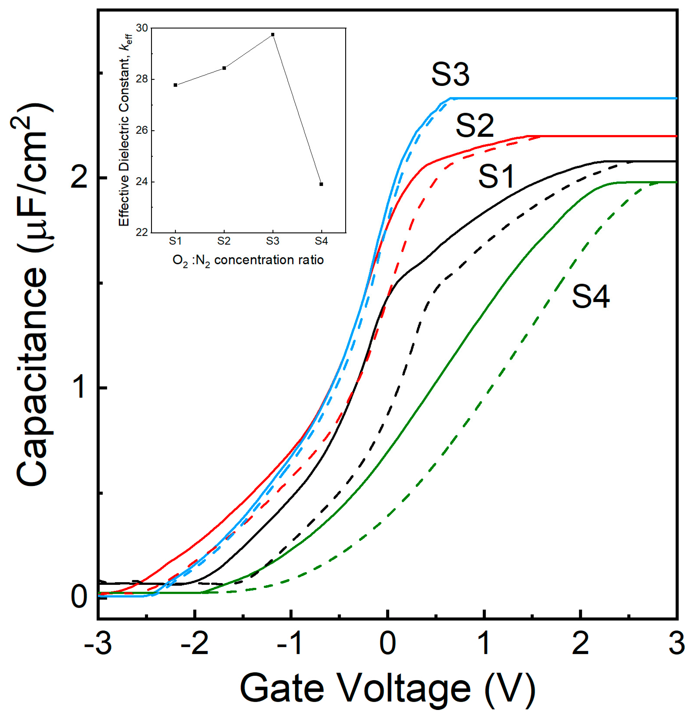
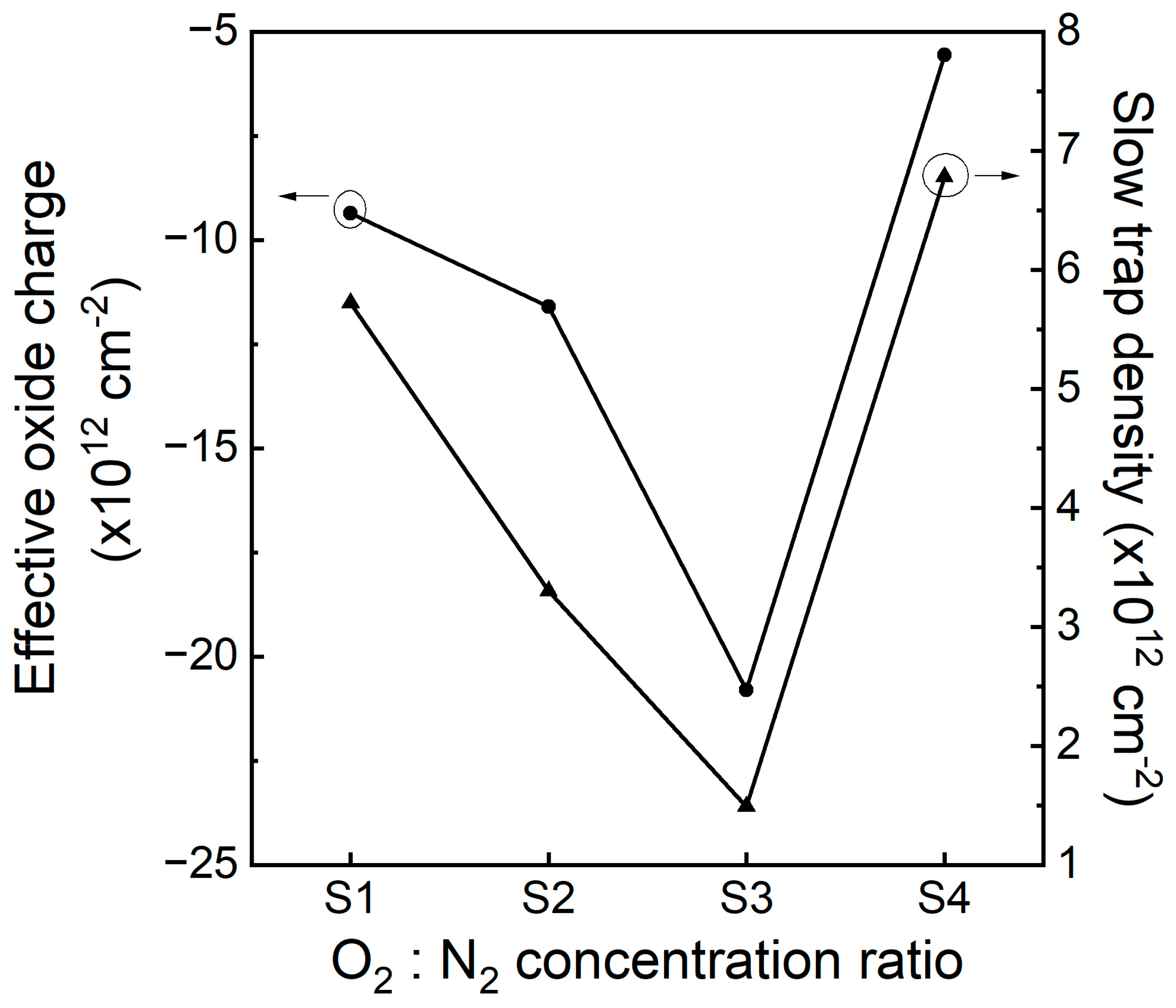
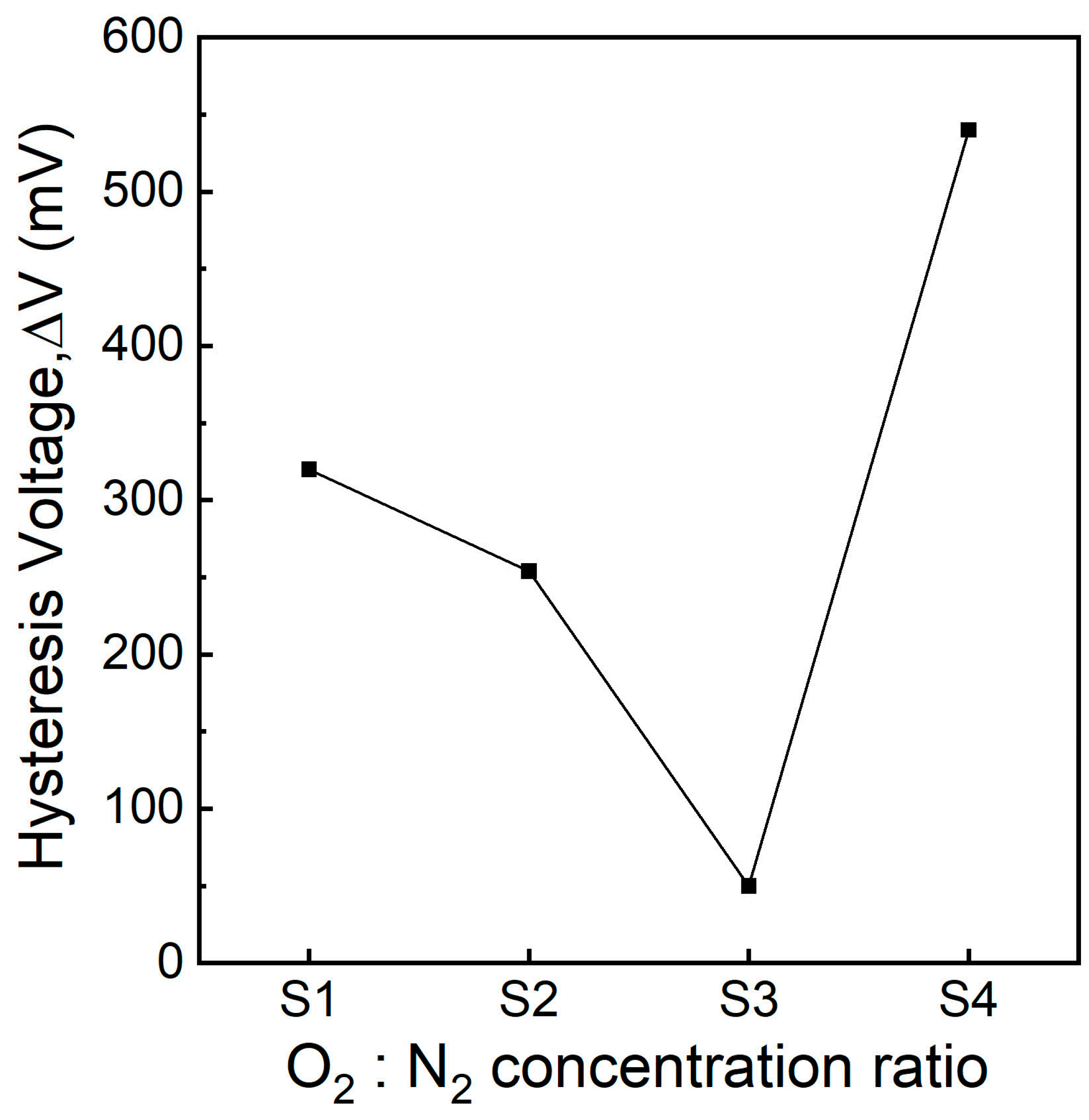
3.5. C-V Characteristics
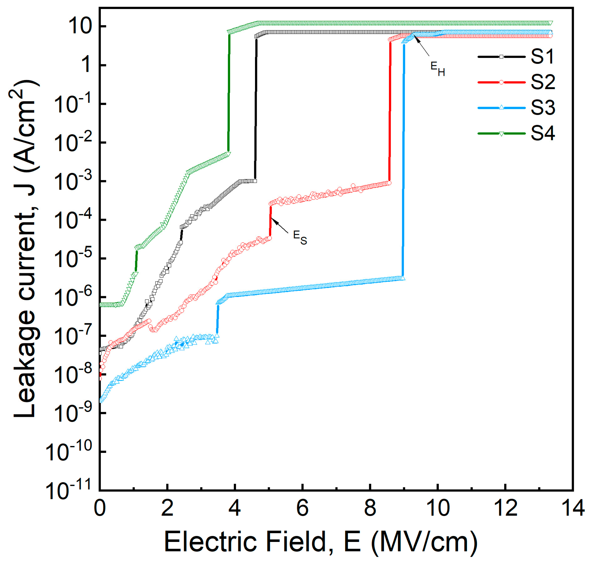
3.6. J-E Characteristics
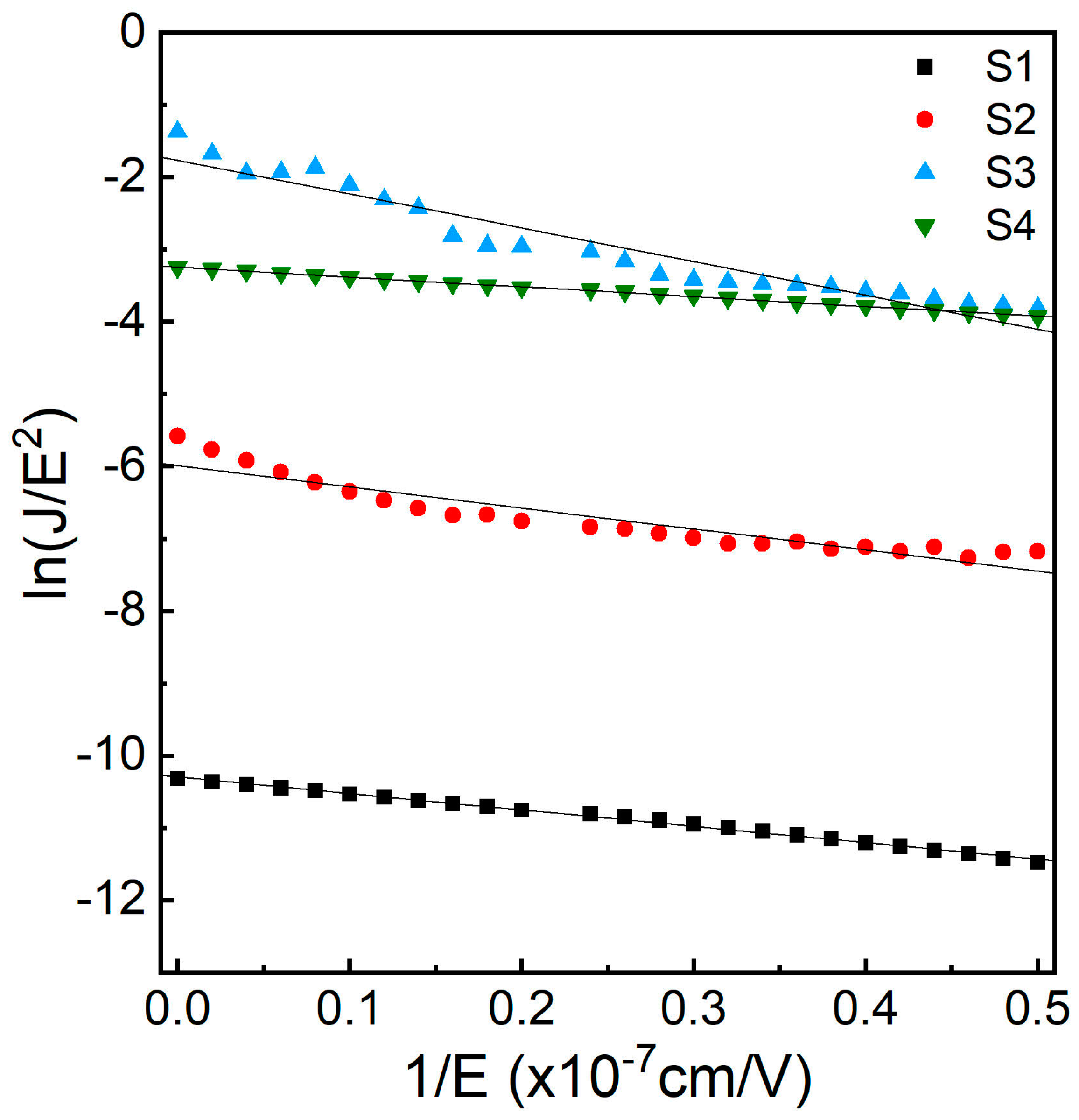
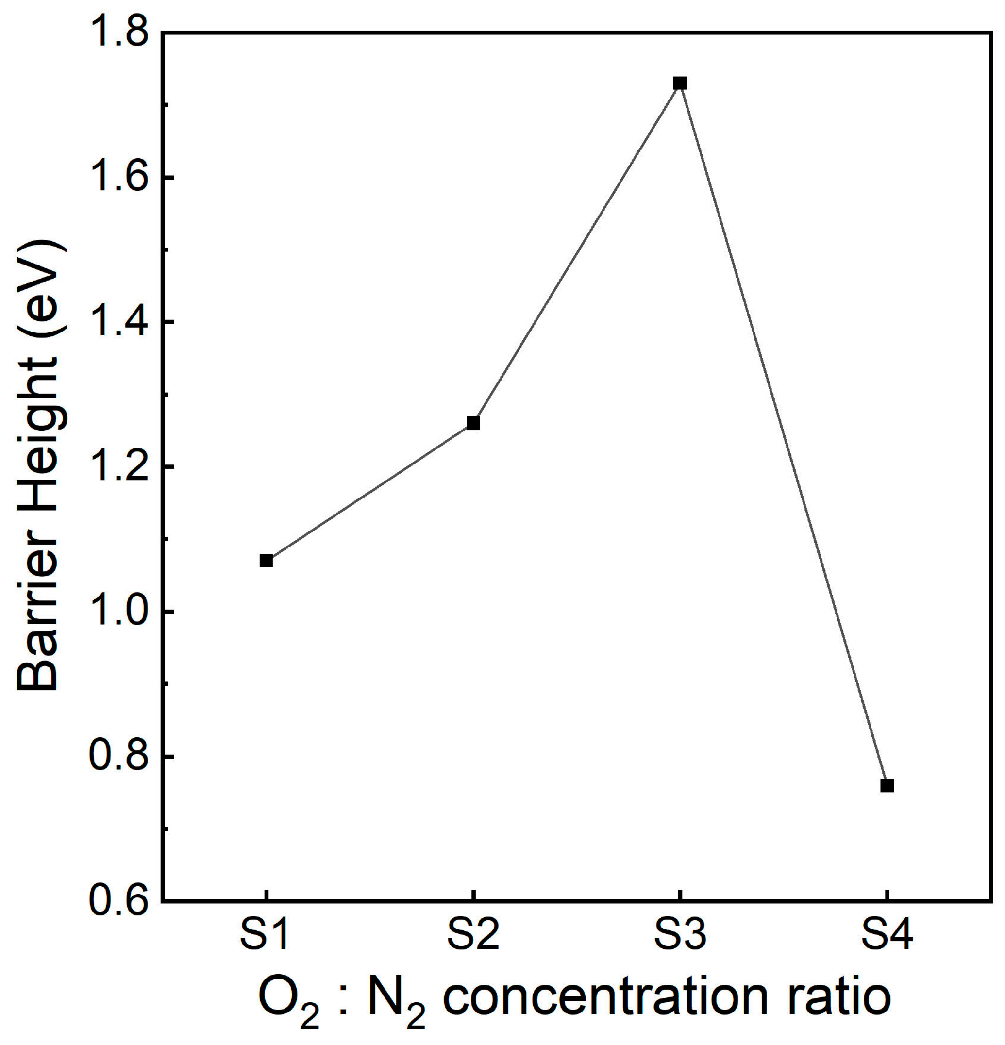
3.7. Fowler–Nordheim Tunnelling Analysis
4. Conclusions
Author Contributions
Funding
Institutional Review Board Statement
Informed Consent Statement
Data Availability Statement
Conflicts of Interest
References
- Majid, A.; Rani, N.; Malik, M.F.; Ahmad, N.; Najam-al, H.; Hussain, F.; Shakoor, A. A review on transition metal doped silicon carbide. Ceram. Int. 2019, 45, 8069–8080. [Google Scholar] [CrossRef]
- Arun Kumar Thilipan, G.; Rao, A. Influence of power on the physical and electrical properties of magnetron sputtered gadolinium oxide thin films for MOS capacitors. Mater. Sci. Semicond. Process. 2021, 121, 105408. [Google Scholar] [CrossRef]
- Wong, Y.H.; Cheong, K.Y. Electrical Characteristics of Oxidized/Nitrided Zr Thin Film on Si. J. Electrochem. Soc. 2011, 158, H1270. [Google Scholar] [CrossRef]
- Deng, J.; Wang, Y.; Quah, H.J. Structural, chemical, and metal-oxide-semiconductor characteristics of RF magnetron sputtered thulium oxide passivation layer on 4H-silicon carbide substrate. Appl. Surf. Sci. 2024, 657, 159819. [Google Scholar] [CrossRef]
- Goley, P.S.; Hudait, M.K. Germanium based field-effect transistors: Challenges and opportunities. Materials 2014, 7, 2301–2339. [Google Scholar] [CrossRef] [PubMed]
- Robertson, J.; Wallace, R.M. High-K materials and metal gates for CMOS applications. Mater. Sci. Eng. R Rep. 2015, 88, 1–41. [Google Scholar] [CrossRef]
- Jayawardhena, I.U.; Ramamurthy, R.P.; Morisette, D.; Ahyi, A.C.; Thorpe, R.; Kuroda, M.A.; Feldman, L.C.; Dhar, S. Effect of surface treatments on ALD Al2O3/4H-SiC metal–oxide–semiconductor field-effect transistors. J. Appl. Phys. 2021, 129, 075702. [Google Scholar] [CrossRef]
- Tanner, C.M.; Choi, J.; Chang, J.P. Electronic structure and band alignment at the HfO2/4H-SiC interface. J. Appl. Phys. 2007, 101, 034108. [Google Scholar] [CrossRef]
- Wong, Y.H.; Cheong, K.Y. Properties of thermally oxidized and nitrided Zr-oxynitride thin film on 4H–SiC in diluted N2O ambient. Mater. Chem. Phys. 2012, 136, 624–637. [Google Scholar] [CrossRef]
- Panda, D.; Tseng, T.-Y. Growth, dielectric properties, and memory device applications of ZrO2 thin films. Thin Solid Films 2013, 531, 1–20. [Google Scholar] [CrossRef]
- Tarek, H.J.A.; Lai, W.C.; Razak, A.B.; Wong, H.Y. Physical Vapour Deposition of Zr-Based Nano Films on Various Substrates: A Review. Curr. Nanosci. 2022, 18, 347–366. [Google Scholar] [CrossRef]
- Ye, G.; Wang, H.; Ji, R. Band alignment between 4H-SiC and atomic-layer-deposited ZrO2 determined by X-ray photoelectron spectroscopy. Appl. Phys. Express 2015, 8, 091302. [Google Scholar] [CrossRef]
- Król, K.; Sochacki, M.; Taube, A.; Kwietniewski, N.; Gierałtowska, S.; Wachnicki, Ł.; Godlewski, M.; Szmidt, J. Influence of atomic layer deposition temperature on the electrical properties of Al/ZrO2/SiO2/4H-SiC metal-oxide-semiconductor structures. Phys. Status Soliodi A 2018, 215, 1700882. [Google Scholar] [CrossRef]
- Kurniawan, T.; Wong, Y.H.; Yew Cheong, K.; Moon, J.H.; Bahng, W.; Abdul Razak, K.; Lockman, Z.; Joon Kim, H.; Kim, N.-K. Effects of post-oxidation annealing temperature on ZrO2 thin film deposited on 4H-SiC substrate. Mater. Sci. Semicond. Process. 2011, 14, 13–17. [Google Scholar] [CrossRef]
- Quah, H.J.; Lim, W.F.; Wimbush, S.C.; Lockman, Z.; Cheong, K.Y. Electrical properties of pulsed laser deposited Y2O3 gate oxide on 4H–SiC. Electrochem. Solid-State Lett. 2010, 13, H396. [Google Scholar] [CrossRef]
- Barhate, V.N.; Agrawal, K.S.; Patil, V.S.; Patil, S.R.; Mahajan, A.M. Performance enhancement of Al/La2O3/ZrO2/4H–SiC MOS device with LaON as interfacial passivation layer. Mater. Sci. Semicond. Process. 2020, 117, 105161. [Google Scholar] [CrossRef]
- Odesanya, K.O.; Onik, T.A.M.; Ahmad, R.; Andriyana, A.; Ramesh, S.; Tan, C.Y.; Wong, Y.H. Physical and electrical characteristics of Ho2O3 thin film based on 4H-SiC wide bandgap semiconductor. Thin Solid Films 2022, 741, 138997. [Google Scholar] [CrossRef]
- Li, S.; Lin, Y.; Tang, S.; Feng, L.; Li, X. A review of rare-earth oxide films as high k dielectrics in MOS devices—Commemorating the 100th anniversary of the birth of Academician Guangxian Xu. J. Rare Earths 2021, 39, 121–128. [Google Scholar] [CrossRef]
- Goh, K.H.; Haseeb, A.S.M.A.; Wong, Y.H. Samarium Oxide and Samarium Oxynitride Thin Film as Alternative Gate Oxide on Silicon Substrate. In Reference Module in Materials Science and Materials Engineering; Elsevier: Amsterdam, The Netherlands, 2017. [Google Scholar] [CrossRef]
- Goh, K.H.; Haseeb, A.S.M.A.; Wong, Y.H. Effect of oxidation temperature on physical and electrical properties of Sm2O3 thin-film gate oxide on Si substrate. J. Electron. Mater. 2016, 45, 5302–5312. [Google Scholar] [CrossRef]
- Pan, T.-M.; Huang, C.-C. Effects of oxygen content and postdeposition annealing on the physical and electrical properties of thin Sm2O3 gate dielectrics. Appl. Surf. Sci. 2010, 256, 7186–7193. [Google Scholar] [CrossRef]
- Onik, T.A.M.; Hawari, H.F.; Sabri, M.F.M.; Wong, Y.H. Growth mechanisms and characteristics of Sm2O3 based on Ge semiconductor through oxidation and nitridation. Appl. Surf. Sci. 2021, 544, 148949. [Google Scholar] [CrossRef]
- Li, S.; Lin, Y.; Li, G.; Yu, H.; Tang, S.; Wu, Y.; Li, X.; Tian, W. Improved dielectric properties of La2O3–ZrO2 bilayer films for novel gate dielectrics. Vacuum 2020, 178, 109448. [Google Scholar] [CrossRef]
- Huang, H.; Wang, Y.; Chen, K.H.; Fei, X.X. Leakage Current Behavior in HfO2/SiO2/Al2O3 Stacked Dielectric on 4H-SiC Substrate. IEEE J. Electron Devices Soc. 2023, 11, 438–443. [Google Scholar] [CrossRef]
- Mavrou, G.; Tsipas, P.; Sotiropoulos, A.; Galata, S.; Panayiotatos, Y.; Dimoulas, A.; Marchiori, C.; Fompeyrine, J. Very high-κ ZrO2 with La2O3 (LaGeOx) passivating interfacial layers on germanium substrates. Appl. Phys. Lett. 2008, 93, 212904. [Google Scholar] [CrossRef]
- Abdul Shekkeer, K.M.; Cheong, K.Y.; Quah, H.J. Effects of post-deposition annealing of cerium oxide passivation layer in nitrogen-oxygen-nitrogen ambient. Int. J. Energy Res. 2022, 46, 14814–14826. [Google Scholar] [CrossRef]
- Zeng, Y.-X.; Wang, X.-R.; Yang, R.-Y.; Huang, W.; Yang, L.; Ma, H.-P.; Zhang, Q.-C. MOS structure with as-deposited ALD Al2O3/4H-SiC heterostructure with high electrical performance: Investigation of the interfacial region. J. Vac. Sci. Technol. A 2024, 42, 053207. [Google Scholar] [CrossRef]
- Chaussende, D.; Tabouret, V.; Crisci, A.; Morais, M.; Coindeau, S.; Berthomé, G.; Kollmuss, M.; Wellmann, P.; Jomard, F.; Pinault-Thaury, M.-A.; et al. Investigation of amorphous-SiC thin film deposition by RF magnetron sputtering for optical applications. Mater. Sci. Semicond. Process. 2024, 182, 108673. [Google Scholar] [CrossRef]
- Khosa, R.Y.; Chen, J.T.; Winters, M.; Pálsson, K.; Karhu, R.; Hassan, J.; Rorsman, N.; Sveinbjörnsson, E.Ö. Electrical characterization of high k-dielectrics for 4H-SiC MIS devices. Mater. Sci. Semicond. Process. 2019, 98, 55–58. [Google Scholar] [CrossRef]
- Robertson, J. Band offsets of wide-band-gap oxides and implications for future electronic devices. J. Vac. Sci. Technol. B. 2000, 18, 1785–1791. [Google Scholar] [CrossRef]
- Kaya, S.; Yilmaz, E.; Karacali, H.; Cetinkaya, A.O.; Aktag, A. Samarium oxide thin films deposited by reactive sputtering: Effects of sputtering power and substrate temperature on microstructure, morphology and electrical properties. Mater. Sci. Semicond. Process. 2015, 33, 42–48. [Google Scholar] [CrossRef]
- Zabidi, A.R.M.; Hassan, Z.; Lim, W.F. Investigation of concurrent flow of nitrogen and oxygen for the oxidation of cerium to cerium oxide films. J. Mater. Sci. Mater. Electron. 2024, 35, 434. [Google Scholar] [CrossRef]
- Wong, Y.H.; Cheong, K.Y. Formation of Zr-oxynitride thin films on 4H-SiC substrate. Thin Solid Films 2012, 520, 6822–6829. [Google Scholar] [CrossRef]
- Odesanya, K.O.; Ahmad, R.; Andriyana, A.; Ramesh, S.; Tan, C.Y.; Wong, Y.H. Effects of O2 and N2 gas concentration on the formation of Ho2O3 gate oxide on 4H-SiC substrate. Silicon 2022, 15, 755–761. [Google Scholar] [CrossRef]
- Wong, Y.H.; Lei, Z.C.; Abidin, N.I.Z. Surface and interface characteristics of annealed ZrO2/Ge oxide-semiconductor structure in argon ambient. Surf. Interfaces 2021, 23, 101007. [Google Scholar] [CrossRef]
- Zhu, L.; He, G.; Li, W.; Yang, B.; Fortunato, E.; Martins, R. Nontoxic, eco-friendly fully water-induced ternary Zr–Gd–O dielectric for high-performance transistors and unipolar inverters. Adv. Electron. Mater. 2018, 4, 1800100. [Google Scholar] [CrossRef]
- Nath, D.; Singh, F.; Das, R. X-ray diffraction analysis by Williamson-Hall, Halder-Wagner and size-strain plot methods of CdSe nanoparticles- a comparative study. Mater. Chem. Phys. 2020, 239, 122021. [Google Scholar] [CrossRef]
- Mote, V.D.; Purushotham, Y.; Dole, B.N. Williamson-Hall analysis in estimation of lattice strain in nanometer-sized ZnO particles. J. Theor. Appl. Phys. 2012, 6, 6. [Google Scholar] [CrossRef]
- Zhang, J.W.; He, G.; Zhou, L.; Chen, H.S.; Chen, X.S.; Chen, X.F.; Deng, B.; Lv, J.G.; Sun, Z.Q. Microstructure optimization and optical and interfacial properties modulation of sputtering-derived HfO2 thin films by TiO2 incorporation. J. Alloys Compd. 2014, 611, 253–259. [Google Scholar] [CrossRef]
- Pirrotta, O.; Larcher, L.; Lanza, M.; Padovani, A.; Porti, M.; Nafría, M.; Bersuker, G. Leakage current through the poly-crystalline HfO2: Trap densities at grains and grain boundaries. J. Appl. Phys. 2013, 114, 134503. [Google Scholar] [CrossRef]
- Dolabella, S.; Borzì, A.; Dommann, A.; Neels, A. Lattice Strain and Defects Analysis in Nanostructured Semiconductor Materials and Devices by High-Resolution X-Ray Diffraction: Theoretical and Practical Aspects. Small Methods 2022, 6, 2100932. [Google Scholar] [CrossRef]
- Kong, P.; Pu, Y.; Ma, P.; Zhu, J. The characterization and properties of mixed Sc2O3/SiO2 films. Thin Solid Films 2020, 714, 138357. [Google Scholar] [CrossRef]
- Tang, X.; Zhu, X.; Dai, J.; Sun, Y. Self-limited grain growth, dielectric, leakage and ferroelectric properties of nanocrystalline BiFeO3 thin films by chemical solution deposition. Acta Mater. 2013, 61, 1739–1747. [Google Scholar] [CrossRef]
- Sasikumar, K.; Bharathikannan, R.; Raja, M.; Mohanbabu, B. Fabrication and characterization of rare earth (Ce, Gd, and Y) doped ZrO2 based metal-insulator-semiconductor (MIS) type Schottky barrier diodes. Superlattices Microstruct. 2020, 139, 106424. [Google Scholar] [CrossRef]
- Lei, Z.C.; Goh, K.H.; Zainal Abidin, N.I.; Wong, Y.H. Effect of oxidation temperature on physical and electrical properties of ZrO2 thin-film gate oxide on Ge substrate. Thin Solid Films 2017, 642, 352–358. [Google Scholar] [CrossRef]
- Deng, J.; Quah, H.J. Structural, morphological, and metal-oxide-semiconductor characteristics of thulium oxide passivation layer grown in nitrogen-oxygen-nitrogen ambient. Sustain. Mater. Technol. 2023, 35, e00534. [Google Scholar] [CrossRef]
- Wong, Y.H.; Cheong, K.Y. Thermal oxidation and nitridation of sputtered Zr thin film on Si via N2O gas. J. Alloys Compd. 2011, 509, 8728–8737. [Google Scholar] [CrossRef]
- Kondaiah, P.; Jagadeesh Chandra, S.V.; Fortunato, E.; Chel Jong, C.; Mohan Rao, G.; Koti Reddy, D.V.R.; Uthanna, S. Substrate temperature influenced ZrO2 films for MOS devices. Surf. Interface Anal. 2020, 52, 541–546. [Google Scholar] [CrossRef]
- Wilk, G.D.; Wallace, R.M.; Anthony, J.M. High-κ gate dielectrics: Current status and materials properties considerations. J. Appl. Phys. 2001, 89, 5243–5275. [Google Scholar] [CrossRef]
- Afanas’ev, V.V.; Bassler, M.; Pensl, G.; Schulz, M.J.; Stein von Kamienski, E. Band offsets and electronic structure of SiC/SiO2 interfaces. J. Appl. Phys. 1996, 79, 3108–3114. [Google Scholar] [CrossRef]
- Afanas’ev, V.V.; Stesmans, A. Valence band offset and hole injection at the 4H-, 6H-SiC/SiO2 interfaces. Appl. Phys. Lett. 2000, 77, 2024–2026. [Google Scholar] [CrossRef]
- Gao, J.; He, G.; Fang, Z.B.; Lv, J.G.; Liu, M.; Sun, Z.Q. Interface quality modulation, band alignment modification and optimization of electrical properties of HfGdO/Ge gate stacks by nitrogen incorporation. J. Alloys Compd. 2017, 695, 2199–2206. [Google Scholar] [CrossRef]
- He, G.; Gao, J.; Chen, H.; Cui, J.; Sun, Z.; Chen, X. Modulating the interface quality and electrical properties of HfTiO/InGaAs gate stack by atomic-layer-deposition-derived Al2O3 passivation Layer. ACS Appl. Mater. Interfaces 2014, 6, 22013–22025. [Google Scholar] [CrossRef]
- Robertson, J. High dielectric constant gate oxides for metal oxide Si transistors. Rep. Prog. Phys. 2006, 69, 327–396. [Google Scholar] [CrossRef]
- Kim, J.-G.; Yoo, S.J.; Kim, C.-Y.; Jou, H.-T. Circular fast fourier transform application: A useful script for fast fourier transform data analysis of high-resolution transmissioctron microscopy image. Appl. Microsc. 2014, 44, 138–143. [Google Scholar] [CrossRef]
- Kita, K.; Toriumi, A. Origin of electric dipoles formed at high-k/SiO2 interface. Appl. Phys. Lett. 2009, 94, 132902. [Google Scholar] [CrossRef]
- Novkovski, N. Modification of the Terman method for determination of interface states in metal–insulator–semiconductor structures. J. Phys. Commun. 2017, 1, 035006. [Google Scholar] [CrossRef]
- Kuznetsova, T.; Lapitskaya, V.; Khabarava, A.; Chizhik, S.; Warcholinski, B.; Gilewicz, A. The influence of nitrogen on the morphology of ZrN coatings deposited by magnetron sputtering. Appl. Surf. Sci. 2020, 522, 146508. [Google Scholar] [CrossRef]
- Choopun, S.; Vispute, R.D.; Noch, W.; Balsamo, A.; Sharma, R.P.; Venkatesan, T.; Iliadis, A.; Look, D.C. Oxygen pressure-tuned epitaxy and optoelectronic properties of laser-deposited ZnO films on sapphire. Appl. Phys. Lett. 1999, 75, 3947–3949. [Google Scholar] [CrossRef]
- Hedei, P.H.M.A.; Hassan, Z.; Quah, H.J. Effects of post-deposition annealing temperature in nitrogen/oxygen/nitrogen ambient on polycrystalline gallium oxide films. Appl. Surf. Sci. 2021, 550, 149340. [Google Scholar] [CrossRef]
- Tarek, A.H.J.; Onik, T.A.M.; Lai, C.W.; Razak, B.A.; Lee, H.W.; Tan, C.K.; Azeem, W.; Wong, Y.H. Bilayer gate dielectric of ZrO2 and Ho2O3 on 4H–SiC substrate: Structural and electrical characterization. J. Mater. Sci. Mater. Electron. 2024, 35, 2151. [Google Scholar] [CrossRef]
- Perkins, C.K.; Jenkins, M.A.; Chiang, T.-H.; Mansergh, R.H.; Gouliouk, V.; Kenane, N.; Wager, J.F.; Conley, J.F., Jr.; Keszler, D.A. Demonstration of Fowler–Nordheim tunneling in simple solution-processed thin films. ACS Appl. Mater. Interfaces 2018, 10, 36082–36087. [Google Scholar] [CrossRef] [PubMed]


| Sample | Gas Concentration |
|---|---|
| S1 | 50% O2:50% N2 |
| S2 | 70% O2:30% N2 |
| S3 | 90% O2:10% N2 |
| S4 | 100% O2 |
| Configuration | Deposition | J at 1 V (A cm−2) | (MV cm−1) | Ref. |
|---|---|---|---|---|
| Ho2O3/SiC | Sputtering | 10−6 | 8.95 | [17] |
| ZrO2/SiC | Sputtering | 10−6 | 5.05 | [9] |
| ZrO2/SiO2/SiC | ALD | ~10−10 | 16 | [13] |
| ZrO2/Ho2O3/SiC | Sputtering | 10−11 | 9.7 | [61] |
| ZrO2/Sm2O3/SiC | Sputtering | 10−9 | 10.1 | This work |
Disclaimer/Publisher’s Note: The statements, opinions and data contained in all publications are solely those of the individual author(s) and contributor(s) and not of MDPI and/or the editor(s). MDPI and/or the editor(s) disclaim responsibility for any injury to people or property resulting from any ideas, methods, instructions or products referred to in the content. |
© 2025 by the authors. Licensee MDPI, Basel, Switzerland. This article is an open access article distributed under the terms and conditions of the Creative Commons Attribution (CC BY) license (https://creativecommons.org/licenses/by/4.0/).
Share and Cite
Jafarul Tarek, A.H.; Mozaffor Onik, T.A.; Lai, C.W.; Abdul Razak, B.; Kee, C.C.; Wong, Y.H. Properties of Bilayer Zr- and Sm-Oxide Gate Dielectric on 4H-SiC Substrate Under Varying Nitrogen and Oxygen Concentrations. Ceramics 2025, 8, 49. https://doi.org/10.3390/ceramics8020049
Jafarul Tarek AH, Mozaffor Onik TA, Lai CW, Abdul Razak B, Kee CC, Wong YH. Properties of Bilayer Zr- and Sm-Oxide Gate Dielectric on 4H-SiC Substrate Under Varying Nitrogen and Oxygen Concentrations. Ceramics. 2025; 8(2):49. https://doi.org/10.3390/ceramics8020049
Chicago/Turabian StyleJafarul Tarek, Ahmad Hafiz, Tahsin Ahmed Mozaffor Onik, Chin Wei Lai, Bushroa Abdul Razak, Chia Ching Kee, and Yew Hoong Wong. 2025. "Properties of Bilayer Zr- and Sm-Oxide Gate Dielectric on 4H-SiC Substrate Under Varying Nitrogen and Oxygen Concentrations" Ceramics 8, no. 2: 49. https://doi.org/10.3390/ceramics8020049
APA StyleJafarul Tarek, A. H., Mozaffor Onik, T. A., Lai, C. W., Abdul Razak, B., Kee, C. C., & Wong, Y. H. (2025). Properties of Bilayer Zr- and Sm-Oxide Gate Dielectric on 4H-SiC Substrate Under Varying Nitrogen and Oxygen Concentrations. Ceramics, 8(2), 49. https://doi.org/10.3390/ceramics8020049