Article

Evolution of Copper Electrodes Fabricated by Electroless Plating on BaZr0.7Ce0.2Y0.1O3-δ Proton-Conducting Ceramic Membrane: From Deposition to Testing in Methane

1
National Renewable Energy Laboratory, Golden, CO 80401, USA
2
Colorado School of Mines, Golden, CO 80401, USA
3
Intel Corporation, Hillsboro, OR 97124, USA
4
Elementum 3D, Erie, CO 80516, USA
*
Authors to whom correspondence should be addressed.
Ceramics 2018, 1(2), 261-273; https://doi.org/10.3390/ceramics1020021
Submission received: 30 August 2018 / Revised: 21 September 2018 / Accepted: 28 September 2018 / Published: 2 October 2018
(This article belongs to the Special Issue Functional Ceramics for Energy Applications)

Abstract

:
We investigated copper electrodes deposited onto a BaZr0.7Ce0.2Y0.1O3-δ (BZCY72) proton-conducting membrane via a novel electroless plating method, which resulted in significantly improved performance when compared to a traditional painted copper electrode. The increased performance was examined with a multiscale multitechnique characterization method including time-of-flight secondary-ion mass spectroscopy (TOF-SIMS), transmission electron microscopy (TEM), scanning spreading-resistance microscopy (SSRM), and atom-probe tomography (APT). Through this method, we observed that a palladium catalyst layer alloys with the copper electrode. We also explored the nature of a non-coking-induced carbon-rich phase that may be involved with the improved performance of the electrode.

Graphical Abstract

1. Introduction

High-temperature proton conductors (HTPCs) have increasingly attracted attention because of their high proton transference number and low activation energy for proton conduction [1,2]. Various applications can be targeted for HTPC-based devices. Examples include protonic ceramic fuel cells (PCFCs) for electricity generation [3,4,5], protonic ceramic electrolysis cells (PCECs) for energy storage [6,7], membranes for hydrogen separation [8], membrane reactors for fuels upgrading (e.g., methane dehydroaromatization–MDA) [9,10], and hydrogen compression [11].
The MDA reaction consists of a single-step, non-oxidative route to produce hydrogen and benzene from methane as given in Equation (1):
6 CH4 ↔ C6H6 + 9 H2
The reaction is typically carried out around 700 °C using a catalyst consisting of molybdenum carbide nanoparticles supported on shape-selective zeolites such as ZSM-5 and MCM-22 [12,13,14]. However, the methane conversion is thermodynamically limited to about ~12% efficiency at 700 °C. The equilibrium can be shifted toward higher yields if hydrogen is removed from the mixture of products, which can be achieved using a HTPC membrane. The process can be promoted by applying an electric potential to drive the hydrogen across the membrane [9] and is referred to as a catalytic membrane reactor (CMR). Morejudo et al. [10] performed CMR measurements using a 20–30-µm-thick, dense layer of BaZr0.7Ce0.2Y0.1O3-δ (BZCY72) electrolyte on a porous BZCY72-Ni cermet, with a Cu anode for the oxidation of hydrogen to protons. Patki et al. [15,16,17] developed Cu electrodes on BZCY72 substrates by electroless plating (ELP) to overcome the major drawbacks of organometallic copper paste, which include thickness (>15 µm) and delamination problems. One-µm-thick Cu electrodes with excellent adhesion to the BZCY72 substrates were obtained by ELP using three catalysts: Pd, Ru, and Cu. The development of the ELP procedure was initially performed on BZCY72 discs (2 cm in diameter, symmetric cell configuration [17]) and the process was later transferred to tubes [15]: BaZr0.7Ce0.2Y0.1O3-δ (BZCY72) electrolyte on a porous BZCY72-Ni support (referred to as BZCY72/Ni//BZCY72).
ELP Cu electrodes with a Pd catalyst deposited on BZCY72/Ni//BZCY72 tubes were tested in similar conditions as the one reported by Morejudo et al. [10]. High faradaic efficiency of the BZCY membrane (80–85%) using this electroless-deposited copper layer was observed [15]. The decrease in faradaic efficiency reported in [
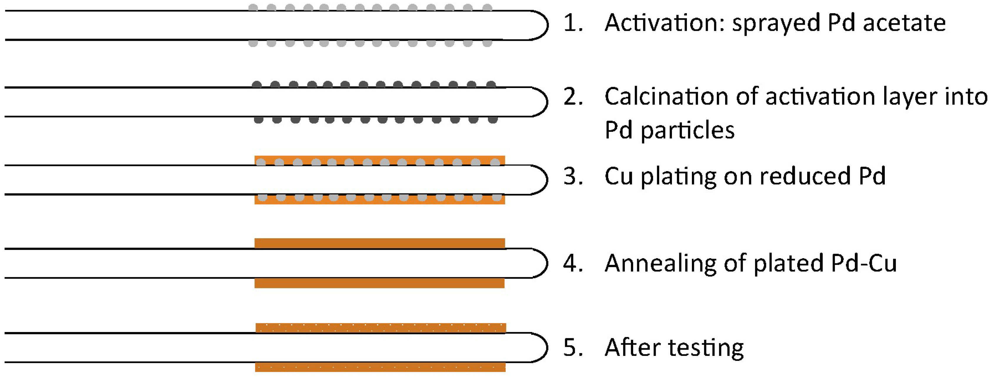
15] with increasing the current density was explained by the history of the BZCY/Ni//BZCY assembly (cerium diffusion from support to electrolyte during sintering) and was not related to the Cu electrode performance. To better understand the role that this electroless copper deposition process plays in the performance, we thoroughly studied the microstructure and composition of the Pd/Cu electrodes at the different stages of the deposition process and after testing (illustrated in Figure 1) using a variety of characterization techniques including: time-of-flight secondary-ion mass spectrometry (TOF-SIMS), transmission electron microscopy (TEM), scanning spreading-resistance microscopy (SSRM), and atom-probe tomography (APT). By using a multitechnique, multiscale characterization approach, we can best assess the reason for the excellent performance observed with the ELP copper electrodes. The TEM can reveal the atomic-scale structure, TOF-SIMS can provide a nanoscale picture of the lateral distribution of dopants and impurities with 100-nm resolution, correspondingly, SSRM can provide local electronic resistivity at the nanoscale, and APT can elucidate the three-dimensional composition of a material with unparalleled, nanometer-scale resolution.

2. Materials and Methods

Tubular substrates (BZCY72/Ni//BZCY72) were obtained from CoorsTek Inc. (Golden, Colorado, CO, USA) and coated with Pd/Cu ELP electrodes as described by Patki et al. [15,16,17]. To better understand the role that this electroless copper deposition process plays in the performance, the microstructure and composition of the Pd/Cu electrodes at the different stages of the deposition process and after testing (illustrated in Figure 1) was thoroughly studied using a variety of characterization techniques outlined in the introduction. Pd acetate in chloroform was sprayed on the tubular substrate (Step 1 in Figure 1). The calcination procedure of the Pd acetate catalyst (Step 2 in Figure 1) was slightly different than that reported by Patki et al. [15,16,17]. The tubes were heated in a dual-atmosphere furnace set-up: dilute hydrogen gas (5% H2 in Ar) was supplied to the inner part of the tube BZCY72-Ni. The gas supplied to the outside of the tube was first nitrogen, while the tube was heated to 800 °C for 15 min then cooled to 400 °C. Subsequently, the gas was switched to air while the temperature was held at 400 °C for 1 h before cooling to room temperature. All the heating and cooling rates were kept at 5 °C∙min−1. The activation layer was then reduced and plated (1 h in a heating bath kept at 55 °C) (Step 3 in Figure 1). The plated sample was then annealed for 4 h at 750 °C in hydrogen (Step 4 in 
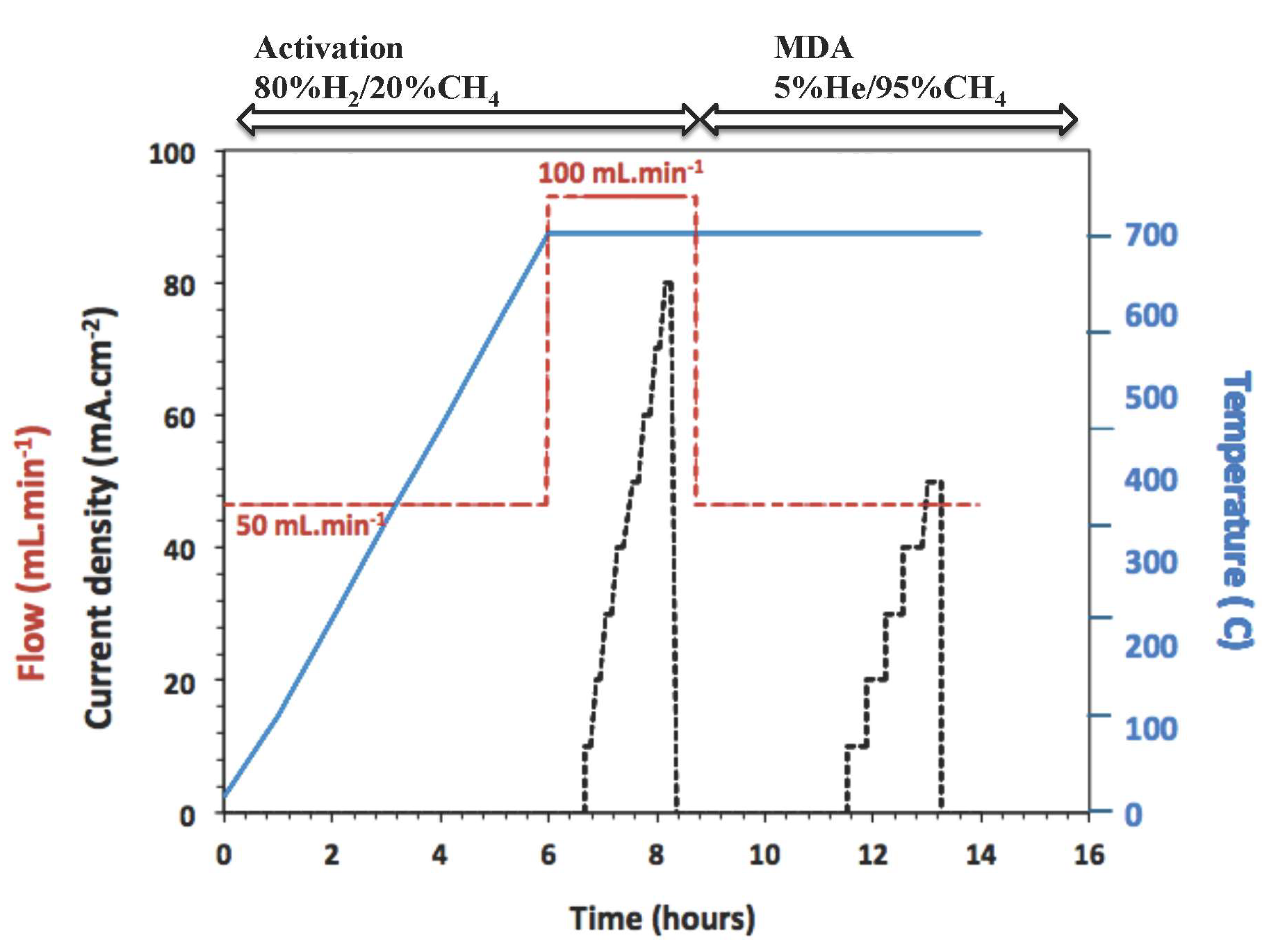
Figure 1) and tested as described in Figure 2; the sample was heated in a catalytic membrane reactor (i.e., with zeolite catalyst on the outer annulus) under 80% hydrogen/20% methane up to 700 °C. The atmosphere was then switched to 95% methane/5% helium at 700 °C and the hydrogen fluxes were measured under MDA conditions at current densities varying from 0 to 80 mA·cm−2. After testing, coking was observed between the BZCY72 membrane and the Pd-Cu electrode, discussed in detail later in the manuscript.
Samples were collected at the various stages of the processing as described in Figure 1 for in-depth characterization. In some cases, the samples were kept as fractured cross-sections; in other cases, the samples were mounted in epoxy and polished down to 1 µm for better finish.
TOF-SIMS measurements were completed using an ION-TOF TOF-SIMS V instrument (Ion-TOF GmbH, Muenster, Germany). SIMS is a powerful analytical technique to determine elemental and isotopic distributions in solids, both organic and inorganic [18,19,20,21]. TOF-SIMS imaging, spectroscopy-mode profiling, and 3-D tomography were used to investigate the role that the palladium activation layer plays in the performance of the membranes which used the electroless plated copper electrode. Secondary ions for analysis were created by a 3-lens 30-keV BiMn ion gun. 3-D tomography was completed using a Bi3++ primary ion-beam cluster (100-ns pulse width, 0.1-pA pulsed beam current); this measurement mode is capable of better than 100-nm lateral-resolution chemical imaging. Standard depth profiling was completed using a Bi+ primary ion beam operated in bunched mode (10-ns pulse width, 1-pA pulsed beam current). An oxygen ion beam with a variable energy from 600 eV to 3 keV was used as the sputtering beam (sputtering current 3–30 nA). After measurements were completed, the sputter craters were measured using an interference light microscope to correlate the sputter time scale to sputter depth.
Secondary-electron micrographs were collected on cross-sections with a JEOL JSM-7000F (JEOL, Tokyo, Japan) scanning electron microscope (SEM). TEM cross-section specimens were prepared using a lift-out technique in an FEI Helios NanoLab 600i. Most of the TEM analyses and energy-dispersive X-ray spectroscopy (EDS) mapping were performed on an FEI Talos F200X instrument (Thermo Fisher Scientific, Hillsboro, Oregon, USA) operated at a 200-kV accelerating voltage. TEM imaging of the APT specimens was performed on a Philips CM200 operated at 200 keV.
SSRM local resistivity imaging is based on the contact-mode atomic force microscope (AFM, Veeco D5000 with Nanoscope V controller). A bias voltage is applied between the probe and sample, and the current flowing through the probe is measured by a logarithm-scale amplifier [22,23]. The probe-sample contact resistance was suppressed by pressing the highly doped diamond-coated tip (Bruker Nano, Santa Barbara, CA, USA) into the sample with a large force (~μN) and applying a high bias voltage (10 V) between the probe and sample. This creates a localized area below the probe that is highly strained and creates dangling bonds, so that the contact resistance is sufficiently lowered. The local spreading resistance just below the probe then dominates the overall measured resistance; the local resistivity of the sample is measured with a resolution comparable to the probe size (~40 nm in this case).
Specimens for APT were milled with a focused ion beam (FIB) in an FEI Helios Nanolab 600i [24]. These specimens were prepared such that consecutive TEM imaging and APT analysis of the tips could be performed [25]. The APT analyses were conducted using laser pulsing in a Cameca LEAP 4000X Si instrument with a 90-mm flight path length at a temperature of 51.4 K, pulse rates of 500–625 kHz, laser energies of 10–55 pJ, a voltage range of 2–8 kV, and detection rate of 5–8 ions per 1000 laser pulses.

3. Results and Discussion

To investigate the root-cause mechanisms for the observed near-doubling of the faradaic efficiency in the ELP coated copper electrode samples compared to standard painted electrodes, samples from all steps of the ELP process outlined in Figure 1 were investigated with a variety of characterization techniques. We focus the discussion on those results which are most revealing to elucidate the mechanism for the observed performance increase.
Figure 3 summarizes a series of SSRM maps taken on a polished cross-section of a membrane ready for testing (Step 4 in Figure 1), as well as some accompanying TEM results of similar areas. The SSRM maps (Figure 3A–C) show areas of high conductivity as bright (Ni phase) and areas of low conductivity as darker (BZCY phase). Figure 3A–C represent the two-phase composite scaffold, the dense BZCY electrolyte, and the BZCY/copper electrode interface, respectively. In Figure 3B, a bright, high-conductivity phase can be seen surrounding a less-conductive BZCY grain. Figure 3D,E are the high-angle annular dark-field (HAADF) scanning TEM image and resulting EDS map for a similar area of the TEM EDS map; results confirm that the high-conductivity phase is nickel-rich at the grain boundaries. These results are consistent with prior observations on samples prepared by solid-state reactive sintering using nickel oxide as a sintering aid: nickel precipitates at the grain-boundaries upon reduction [26,27]. This illustrates the strength of the multitechnique approach taken in this work—that by a combination of techniques, we can obtain nanoscale information about the structure, chemistry, and electrical properties of the material.
TOF-SIMS 3-D tomography is accomplished by collecting a high-resolution chemical image of the sample, then sputtering away some tens to hundreds of nanometers of material, then imaging again. Through these subsequent imaging and sputtering steps, one can build up a 3-D chemical reconstruction of a small area of the sample. As an illustration of the strength of TOF-SIMS tomography in revealing the spatial distribution of impurities, the 3-D dataset in Figure 4A,B shows the distribution of the two phases in the BZCY/NiO scaffold for the dense BZCY membrane. Figure 4C presents the distribution of an impurity (sodium in this case), which shows that the impurity accumulates at the boundaries between the two phases in the two-phase scaffold.
Due to the known propensity for Ni precipitating at the grain boundaries in BZCY [26,27], as illustrated in the SSRM and TEM data in Figure 3, it was unclear if the palladium catalyst layer (Step 1 in 
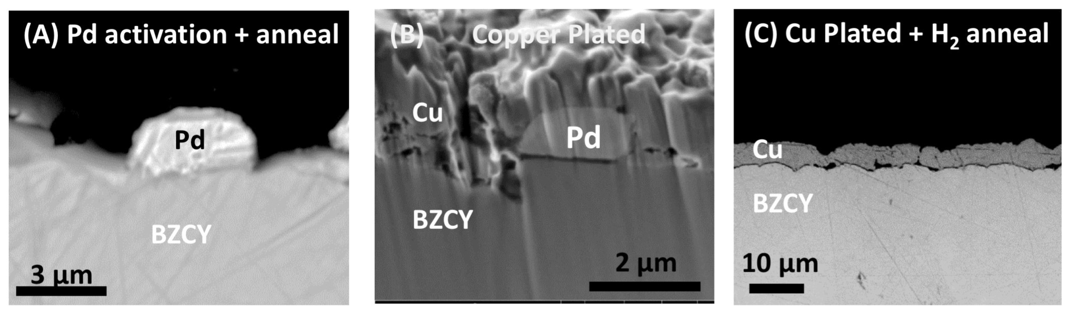
Figure 1) would also migrate to grain boundaries in the BZCY electrolyte after the high-temperature annealing of the copper electrode or during testing. The SEM images in Figure 5 confirm that the Pd particles, which act as a catalyst for the electroless copper deposition, do not remain as discrete Pd particles after the high-temperature anneal to form the Cu electrode. However, the TEM-EDS data (not shown), with detection limits on the order of one atomic percent, are not able to elucidate the spatial distribution of Pd in the material beyond the copper plating step (Step 3 in Figure 1). TOF-SIMS, with detection limits on the order of ppm or better, can thus be used to examine the spatial distribution of the palladium through the entire process of the electroless-deposited copper electrode. TOF-SIMS tomography data for palladium during all steps of the electroless-deposited copper electrode deposition process and after testing are shown in Figure 6A–F. The data in Figure 6 are presented in two rows: the upper and lower rows are the same dataset, the top row is the 3-D reconstruction viewed from the top, and the bottom row is the same reconstruction viewed from the side. Each reconstruction is 25 µm × 25 µm in size, and 2–3 µm in depth. The data in Figure 6, and subsequent TOF-SIMS data, are presented on a blue-to-red intensity scale, as shown in the figure on the right-hand side. While white indicates no counts were detected in that area of the dataset, blue represents low intensity measured, while red would be the highest intensity measured for that dataset. The approximate location of the interface between the copper electrode and the BZCY electrolyte is seen in the bottom row of images where the palladium signal begins to decrease. The discrete palladium particles used to catalyze the electroless copper deposition are visible in the copper electrode after the Pd particle deposition step (Figure 6A,B), and also after the copper electrode deposition (Figure 6C,D). Figure 6E,F show that after the high-temperature anneal in a reducing atmosphere, the palladium appears more evenly distributed through the copper electrode, which indicates that the palladium has alloyed with the copper electrode. The palladium alloying is further illustrated in TOF-SIMS data in Supplementary Figure S1. One potential explanation for the high faradaic efficiency that has been observed with electrodes made via this electroless process is if a Pd-based phase that is proton-conducting but not electronically conductive is formed at the interface BZCY/Cu electrode (preventing potential electronic leakage [28]). However, the data in Figure 6 show a uniform Pd/Cu electrode (alloy). Thus, the observed performance is the result of a different mechanism. The SSRM also showed that the average resistance of the copper electrode increases after testing, consistent with a decrease in conductivity expected with copper–palladium alloying [29].
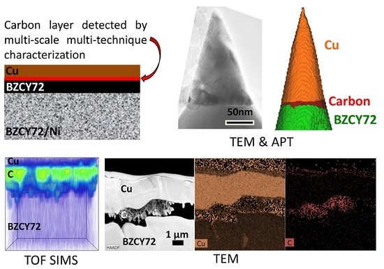
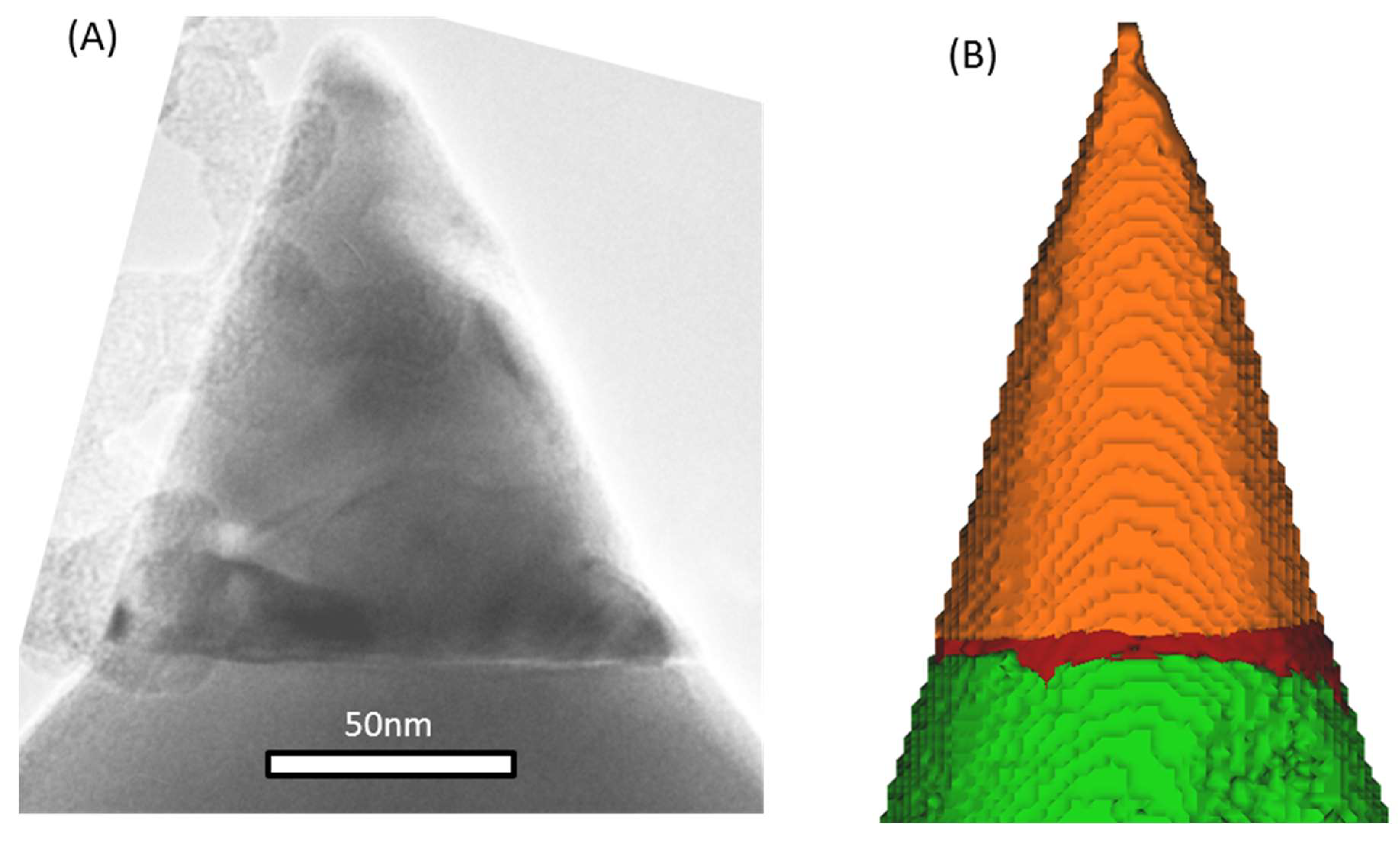
The excellent performance of the electrode is clearly not due to a nonuniform Pd distribution at the Cu/BZCY interface, so the exact mechanism enabling this superior performance required further investigation. The presence of a carbon-rich phase was noted in the samples prepared with the Cu-ELP technique, and we performed additional characterization to investigate this further. APT and TEM data of the sample after the copper plating (Step 3 of Figure 1) in Figure 7 show that a carbon-rich phase is already present at the Cu/BZCY interface immediately after the copper plating step. Additional APT data on a second area of the same sample show identical results, presented in the Supplementary Materials. This suggests that the formation of this interface carbon layer is somehow inherently part of the electrodeposition process. In addition, SSRM did not reveal the presence of a highly electrically conductive phase between the ELP copper electrode and BZCY. This presents another interesting theory for the excellent performance of the observed electrodes: if this carbon-rich phase present at the Cu/BZCY interface blocks electrons but permits proton transport, it could be the reason for the high faradaic efficiency observed experimentally with ELP copper electrode samples.
Using TOF-SIMS tomography, we were able to track the distribution and morphology of this carbon-rich phase throughout processing and after testing. These data are presented in Figure 8, where the carbon-rich phase is detected with TOF-SIMS within the entire copper electrode thickness, as well as at the Cu/BZCY interface. More importantly, as seen in Figure 8D after testing, the phase becomes more concentrated at the Cu/BZCY interface. The TOF-SIMS data were taken under measurement conditions that would not yield good depth resolution; thus, the exact interface between the copper and BZCY as seen in the APT data is difficult to observe in the data. However, the data on the tested sample shown in Figure 8D after testing show an apparent concentration of the carbon-rich phase. From these results, it is unclear if this phase that is concentrated at the Cu/BZCY interface after testing is simply a result of coking from the testing environment. To further investigate this, TOF-SIMS and TEM measurements were performed on BZCY samples with the traditional painted + fired copper electrodes before testing and after testing. The TOF-SIMS 3-D reconstruction of the carbon-rich phase for the painted copper electrode samples is shown in Figure 9, where the data for the electroless plated copper at identical process steps are also shown for direct comparison. It is clear that there is a vastly different distribution of this phase in the electroless plated copper: there is much more carbon throughout the electrode for the electroless copper film prior to testing, and there is a continuous amount of the phase noted at the Cu/BZCY interface after testing in the electroless film compared to the discrete and non-continuous carbon-rich areas at the Cu/BZCY interface noted for the painted copper film tested under similar conditions. TEM results from the same specimen presented in Figure 10 confirm the presence of this carbon-rich phase at the interface between the electrodeposited copper and the BZCY electrolyte after testing. The TEM results and STEM-EDS maps of the carbon-rich phase at the interface between the copper electrode and the BZCY indicate that this phase is mostly carbon and oxygen. The carbon layer in Figure 10 appears noncontinuous due to a preferential milling of the carbon during FIB prep of the TEM specimen. One must keep in mind that Pd is more prone to coking than Cu [30,31,32], and previous analysis reported about 12 wt % of Pd in the Cu electrode, indicating that it would be more prone to coking than a pure copper electrode [16]. However, this increased palladium content is unlikely the explanation for the presence of carbon in the ELP Cu layer. Indeed, the TOF-SIMS data in Figure 8 and the APT results in Figure 7 show that carbon is already present in the electroless plated electrode before testing, and the TOF-SIMS data in Figure 9 show that it is present in much higher amounts than for the copper-paste sample. This is sensible because electroless plating uses organics such as EDTA, glycine, or metal-organic precursors during the deposition process. The TOF-SIMS and TEM data shown in Figure 9 and Figure 10 illustrate that this phase becomes more concentrated at the Cu/BZCY interface during testing in a hydrocarbon-rich atmosphere.
Further study is needed to definitively explain the connection between the observed compositional structure and the near-doubling of the faradaic efficiency seen for the Cu electroless plated electrodes when comparing to standard painted electrodes. However, this study proves the presence of carbon in the plated electrodes before testing. In addition, this develops into a carbon-rich phase at the Cu/BZCY interface, which becomes more concentrated with testing. Far less carbon has been observed for the standard painted copper electrodes, suggesting a key link to performance.

4. Conclusions

A high faradaic efficiency has been observed in BZCY membranes prepared with electroless copper deposited electrodes [15]. Through in-depth characterization, we observed that this performance is not due to a palladium-rich electron-blocking layer at the Cu/BZCY interface. The palladium catalyst layer, required for the electroless copper deposition, alloys with the copper electrode through the subsequent high-temperature processing for electrode formation. Using TOF-SIMS, TEM, and APT, we observed the presence of a carbon-rich phase both in the copper film and at the BZCY/Cu interface that is inherent to the samples with the electroless-deposited copper electrodes but not present in samples with painted copper electrodes. The carbon-rich phase persists after testing and remains present at the Cu/BZCY interface. This suggests that the carbon-rich phase could be related to the observed high faradaic efficiency. These results also illustrate the benefits of using a multitechnique characterization approach to understand the mechanisms underlying changes in performance in proton-conducting membranes.

Supplementary Materials

The following are available online at https://www.mdpi.com/2571-6131/1/2/21/s1. Figure S1: TOF-SIMS 3-D tomography overlay for an ELP copper-plated sample after hydrogen gas anneal (Step 4 of Figure 1). Figure S2: TEM image and APT reconstruction of the interface between the copper electrode (orange) and the dense BZCY electrolyte (green) for a sample after copper plating (Step 3 of Figure 1); second area of analysis.

Author Contributions

S.P.H. contributed to the work by collecting TOF-SIMS data, interpreting the data from TOF-SIMS as well as all the data from the project, in addition to preparing the majority of the manuscript. S.R. contributed by coordinating the research direction and providing membrane samples, as well as partial preparation of the manuscript. D.R.D. performed the TEM and APT measurements and analysis, with assistance and oversight from B.G., C.-S.J. performed the SSRM measurements and analysis. N.S.P. assisted in preparing the ELP copper electrodes and interpreting the results. A.M. provided research direction and assisted in interpreting the results. M.A.-J. also provided research direction and assisted in interpreting the results. All authors contributed to a review of the manuscript before submission.

Funding

This work was supported by the U.S. Department of Energy under Contract No. DE-AC36-08GO28308 with Alliance for Sustainable Energy, LLC, the Manager and Operator of the National Renewable Energy Laboratory. This work was supported by the Laboratory Directed Research and Development (LDRD) Program at the National Renewable Energy Laboratory. NREL is a national laboratory of the U.S. Department of Energy Office of Energy Efficiency and Renewable Energy operated by the Alliance for Sustainable Energy, LLC. The U.S. Government retains and the publisher, by accepting the article for publication, acknowledges that the U.S. Government retains a nonexclusive, paid-up, irrevocable, worldwide license to publish or reproduce the published form of this work, or allow others to do so, for U.S. Government purposes. The authors gratefully acknowledge financial support for this research from CoorsTek Inc., Golden, CO, USA.

Acknowledgments

The authors would also like to thank Christian Kjølseth (CoorsTek Membrane Sciences, Oslo) for sharing the data used in Figure 2 and for proofreading the manuscript.

Conflicts of Interest

The authors declare no conflict of interest.

References

  1. Fabbri, E.; Pergolesi, D.; Traversa, E. Materials challenges toward proton-conducting oxide fuel cells: A critical review. Chem. Soc. Rev. 2010, 39, 4355–4369. [Google Scholar] [CrossRef] [PubMed]
  2. Kreuer, K.D. Proton-Conducting Oxides. Annu. Rev. Mater. Res. 2003, 33, 333–359. [Google Scholar] [CrossRef]
  3. Bi, L.; Boulfrad, S.; Traversa, E. Steam electrolysis by solid oxide electrolysis cells (SOECs) with proton-conducting oxides. Chem. Soc. Rev. 2014, 43, 8255–8270. [Google Scholar] [CrossRef] [PubMed]
  4. Iwahara, H.; Esaka, T.; Uchida, H.; Maeda, N. Proton conduction in sintered oxides and its application to steam electrolysis for hydrogen production. Solid State Ionics 1981, 3, 359–363. [Google Scholar] [CrossRef]
  5. Malavasi, L.; Fisher, C.A.J.; Islam, M.S. Oxide-ion and proton conducting electrolyte materials for clean energy applications: Structural and mechanistic features. Chem. Soc. Rev. 2010, 39, 4370–4387. [Google Scholar] [CrossRef] [PubMed]
  6. Iwahara, H.; Asakura, Y.; Katahira, K.; Tanaka, M. Prospect of Hydrogen Technology Using Proton-Conducting Ceramics. Solid State Ionics 2004, 168, 299–310. [Google Scholar] [CrossRef]
  7. Norby, T.; Larring, Y. Mixed hydrogen ion–electronic conductors for hydrogen permeable membranes. Solid State Ionics 2000, 136, 139–148. [Google Scholar] [CrossRef]
  8. Polfus, J.M.; Wen, X.; Marie-laure, F.; Denonville, C.; Bredesen, R. Oxygen and Hydrogen Separation Membranes Based on Dense Ceramic Conductors, in Membrane Science and Technology; Elsevier: Amsterdam, The Netherlands, 2008; pp. 401–458. [Google Scholar]
  9. Karakaya, C.; Morejudo, S.H.; Zhu, H.; Kee, R.J. Catalytic Chemistry for Methane Dehydroaromatization (MDA) on a Bifunctional Mo/HZSM-5 Catalyst in a Packed Bed. Ind. Eng. Chem. Res. 2016, 55, 9895–9906. [Google Scholar] [CrossRef]
  10. Morejudo, S.H.; Zanón, R.; Escolástico, S.; Yuste-Tirados, Y.; Malerød-Fjeld, H.; Vestre1, P.K.; Coors, W.G.; Martínez, A. Direct conversion of methane to aromatics in a catalytic co-ionic membrane reactor. Science 2016, 353, 563–566. [Google Scholar] [CrossRef] [PubMed] [Green Version]
  11. Malerød-Fjeld, H.; Clark, D.; Yuste-Tirados, I.; Zanón, R.; Catalán-Martinez, D.; Beeaff, D.; Morejudo, S.H.; Vestre, P.K.; Norby, T.; Haugsrud, R.; et al. Thermo-electrochemical production of compressed hydrogen from methane with near-zero energy loss. Nat. Energy 2017, 2, 923–931. [Google Scholar] [CrossRef]
  12. Gao, J.; Zheng, Y.; Jehng, J.M.; Tang, Y.; Wachs, I.E.; Podkolzin, S.G. Identification of molybdenum oxide nanostructures on zeolites for natural gas conversion. Science 2015, 348, 686–690. [Google Scholar] [CrossRef] [PubMed]
  13. Ma, D.; Wang, D.; Su, L.; Shu, Y.; Xu, Y.; Bao, X. Carbonaceous Deposition on Mo/HMCM-22 Catalysts for Methane Aromatization: A TP Technique Investigation. J. Catal. 2002, 208, 260–269. [Google Scholar] [CrossRef]
  14. Xu, Y.; Bao, X.; Lin, L. Direct conversion of methane under nonoxidative conditions. J. Catal. 2003, 216, 386–395. [Google Scholar] [CrossRef] [Green Version]
  15. Patki, N.S.; Manerbino, A.; Way, J.D.; Ricote, S. Galvanic hydrogen pumping performance of copper electrodes fabricated by electroless plating on a BaZr0.9−xCexY0.1O3−δ proton-conducting ceramic membrane. Solid State Ionics 2018, 317, 256–262. [Google Scholar] [CrossRef]
  16. Patki, S.N.; Ricote, S.; Way, J.D. Fabrication of reducing atmosphere electrodes (fuel electrodes) by electroless plating of copper on BaZr0.9−xCexY0.1O3−δ—A proton-conducting ceramic. Int. J. Hydrogen Energy 2017, 42, 16911–16919. [Google Scholar] [CrossRef]
  17. Patki, S.N.; Way, J.D.; Ricote, S. High performance fuel electrodes fabricated by electroless plating of copper on BaZr0.8Ce0.1Y0.1O3-δ proton-conducting ceramic. J. Power Sources 2017, 365, 399–407. [Google Scholar] [CrossRef]
  18. De Souza, R.A.; Martin, M. Secondary Ion Mass Spectrometry (SIMS)—A Powerful Tool for Studying Mass Transport over Various Length Scales. Phys. Status Solid 2007, 4, 1785–1801. [Google Scholar] [CrossRef]
  19. Wilson, G.R.; Stevie, F.A.; Magee, C.W. Secondary Ion Mass Spectrometry: A Practical Handbook for Depth Profiling and Bulk Impurity Analysis; Wiley: Hoboken, NJ, USA, 1989. [Google Scholar]
  20. De Souza, R.A.; Martin, M. Probing Diffusion Kinetics with Secondary Ion Mass Spectrometry. MRS Bull. 2009, 34, 907–914. [Google Scholar] [CrossRef]
  21. Harvey, S.P.; Li, Z.; Christians, J.A.; Zhu, K.; Luther, J.M.; Berry, J.J. Probing Perovskite Inhomogeneity beyond the Surface: TOF-SIMS Analysis of Halide Perovskite Photovoltaic Devices. ACS Appl. Mater. Interfaces 2018, 10, 28541–28552. [Google Scholar] [CrossRef] [PubMed]
  22. Eyben, P.; Clemente, F.; Vanstreels, K.; Pourtois, G.; Clarysse, T.; Duriau, E.; Hantschel, T. Analysis and modeling of the high vacuum scanning spreading resistance microscopy nanocontact on silicon. J. Vac. Sci. Technol. B 2010, 28, 401–406. [Google Scholar] [CrossRef]
  23. Eyben, P.; Denis, S.; Clarysse, T.; Vandervorst, W. Progress towards a physical contact model for scanning spreading resistance microscopy. Mater. Sci. Eng. B 2003, 102, 132–137. [Google Scholar] [CrossRef]
  24. Thompson, K.; Denis, S.; Clarysse, T.; Vandervorst, W. In situ site-specific specimen preparation for atom probe tomography. Ultramicroscopy 2007, 107, 131–139. [Google Scholar] [CrossRef] [PubMed]
  25. Gorman, B.P.; Diercks, D.; Salmon, N.; Stach, E. Hardware and Techniques for Cross-Correlative TEM and Atom Probe Analysis. Microsc. Today 2008, 16, 42–48. [Google Scholar] [CrossRef]
  26. Coors, W.G.; Manerbino, A.; Martinefski, D.; Ricote, S. Fabrication of yttrium-doped barium zirconate for high performance protonic ceramic membranes. In Perovskite Materials—Synthesis, Characterisation, Properties, and Applications; Pan, L., Zhu, G., Eds.; InTech: London, UK, 2016. [Google Scholar]
  27. Ricote, S.; Bonanos, N.; Manerbino, A.; Sullivan, N.P.; Coors, W.G. Effects of the fabrication process on the grain-boundary resistance in BaZr0.9Y0.1O3−δ. J. Mater. Chem. A 2014, 2, 16107–16115. [Google Scholar] [CrossRef]
  28. Dippon, M.; Babiniec, S.M.; Ding, H.; Ricote, S.; Sullivan, N.P. Exploring electronic conduction through BaCexZr0.9−xY0.1O3−d proton-conducting ceramics. Solid State Ionics 2016, 286, 117–121. [Google Scholar] [CrossRef]
  29. Ho, C.Y.; Ackerman, M.W.; Wu, K.Y.; Havill, T.N.; Bogaard, R.H.; Matula, R.A.; Oh, S.G.; James, H.M. Electrical Resistivity of Ten Selected Binary Alloy Systems. J. Phys. Chem. Ref. Data 1983, 12, 183–322. [Google Scholar] [CrossRef] [Green Version]
  30. McLellan, R.B. The solubility of carbon in solid gold, copper, and silver. Scr. Met. 1969, 3, 389–391. [Google Scholar] [CrossRef]
  31. Yokoyama, H.; Numakura, H.; Koiwa, M. The solubility and diffusion of carbon in palladium. Acta Mater. 1998, 46, 2823–2830. [Google Scholar] [CrossRef]
  32. Siller, H.R.; Oates, W.A.; McLellan, R.B. The solubility of carbon in palladium and platinum. J. Less Common. Met. 1968, 16, 71–73. [Google Scholar] [CrossRef]
Figure 1. Stages at which the BZCY72-Pd/Cu electrode interface was investigated with advanced characterization including time-of-flight secondary-ion mass spectrometry (TOF-SIMS), transmission electron microscopy (TEM), scanning spreading-resistance microscopy (SSRM), and atom-probe tomography (APT).
Ceramics 01 00021 g001
Figure 2. Procedure for the catalytic membrane reactor test on the BZCY72/Ni//BZCY72//PdCu tubular sample.
Ceramics 01 00021 g002
Figure 3. SSRM results of a polished cross-section of the completed device before testing (Step 4 in Figure 1) and related TEM results from the same processing step. (A) SSRM map (10 µm × 10 µm) of the two-phase composition scaffold; the high-conductivity Ni phase appears bright. (B) SSRM map (10 µm × 10 µm) of the dense BZCY membrane; a high-conductivity phase is seen at the grain boundaries. (C) SSRM map of the BZCY/copper electrode interface. No evidence for a phase with different electronic conductivity is observed between the BZCY/and copper electrode. (D) STEM high-angle annular dark-field (HAADF) image of several grain boundaries in the dense BZCY/membrane. (E) corresponding STEM EDS map of the image in D, showing a nickel-rich phase at the grain boundaries of the BZCY electrolyte.
Ceramics 01 00021 g003
Figure 4. TOF-SIMS 3-D tomography results investigating a cross-section of the BaZr0.7Ce0.2Y0.1O3-δ (BZCY72)/Ni 2-phase composite support for the dense BZCY electrolyte, illustrating the strength of TOF-SIMS to elucidate the distribution of impurities in the materials. (A) Barium signal (from BZCY ceramic phase); (B) Nickel signal; (C) Impurity signal seen accumulating at the interface between BZCY and Ni in the composite (sodium in this case).
Ceramics 01 00021 g004
Figure 5. Backscattered electron images (A&C), and secondary electron image (B) of the palladium catalyst particles during various steps in the electroless deposition process. (A) discrete palladium particles are observed after activation and calcination (Step 2 in Figure 1); (B) discrete palladium particles are observed under the deposited copper electrode (Step 3 in Figure 1); (C) no discrete palladium particles are observed after the annealing of the copper electrode (Step 4 in Figure 1).
Ceramics 01 00021 g005
Figure 6. TOF-SIMS 3-D tomography results showing the palladium signal at various processing steps. The same dataset is shown in the top and bottom images for (AC), with the top image showing the top view of the dataset, and the bottom images showing the side view. The intensity data is on a blue-to-red colorscale, which is presented at the right. (A,B) After the palladium activation step, discrete palladium particles are observed on the surface (Step 2 in Figure 1). (C,D) After copper plating, discrete palladium particles are still observed under the deposited copper electrode (Step 3 in Figure 1). (E,F) After the annealing of the copper electrode (Step 4 in Figure 1), no discrete palladium particles are observed; the palladium appears to have alloyed with the copper electrode.
Ceramics 01 00021 g006
Figure 7. (A) Transmission electron microscopy image and (B) atom probe tomography reconstruction of the interface between the copper electrode (orange) and the dense BZCY electrolyte (green) for a sample after copper plating (Step 3 of Figure 1). A carbon-rich phase (red) is observed at the interface between the electrode and the electrolyte, consistent with the TOF-SIMS data.
Ceramics 01 00021 g007
Figure 8. TOF-SIMS 3-D tomography results showing the signal from a carbon-rich phase (C2+ secondary ion signal) at various processing steps. The same dataset is shown in the top and bottom images for (AD), with the top image showing the top view of the dataset, and the bottom image showing the side view. The intensity data is on a blue-to-red colorscale, which is presented at the right. (A) After the palladium activation step, the carbon-rich phase is uniformly distributed near the surface palladium layer. (B) After the copper plating step, the carbon-rich phase persists through the electrode thickness. (C) After the anneal in reducing atmosphere, the carbon-rich phase persists as uniformly distributed through the electrode thickness. (D) After testing, the carbon-rich phase is more concentrated at the electrode/BZCY interface.
Ceramics 01 00021 g008
Figure 9. TOF-SIMS 3-D tomography results showing the signal from a carbon-rich phase (C2+ secondary ion signal) at various processing steps for a copper electrode deposited by the electroless method described in this work, as well as the conventional means of painted copper paste. The same dataset is shown in the top and bottom images for (AD), with the top image showing the top view of the dataset, and the bottom image showing the side view. The intensity data is on a blue-to-red colorscale, which is presented at the right. (A) Electroless copper after hydrogen gas anneal (Step 4 of Figure 1); (B) Painted copper after a similar hydrogen gas anneal; the amount and distribution of the carbon-rich phase is vastly different compared to A; (C) Electroless copper after testing; (D) Painted copper after testing; the amount and distribution of the carbon-rich phase is vastly different compared to Figure 9C. These results suggest that the carbon-rich phase observed here is unique to the electroless copper deposition process and is not simply the result of coking during testing.
Ceramics 01 00021 g009
Figure 10. TEM and STEM EDS results of a carbon-rich phase located between the copper electrode and the BZCY electrolyte after testing (Step 5 of Figure 1). The carbon rich phase appears non-continuous due to preferential milling with the FIB during TEM specimen preparation. The HAADF STEM image is in the upper left, and the STEM EDS maps of the same area (each frame labeled with the signal) are shown in the subsequent frames. The apparent low concentration of copper observed in the BZCY layer is the result of a background signal in BZCY.
Ceramics 01 00021 g010

