
In-Process Cutting Temperature Monitoring Method Based on Impedance Model of Dielectric Coating Layer at Tool-Chip Interface


Abstract
:1. Introduction
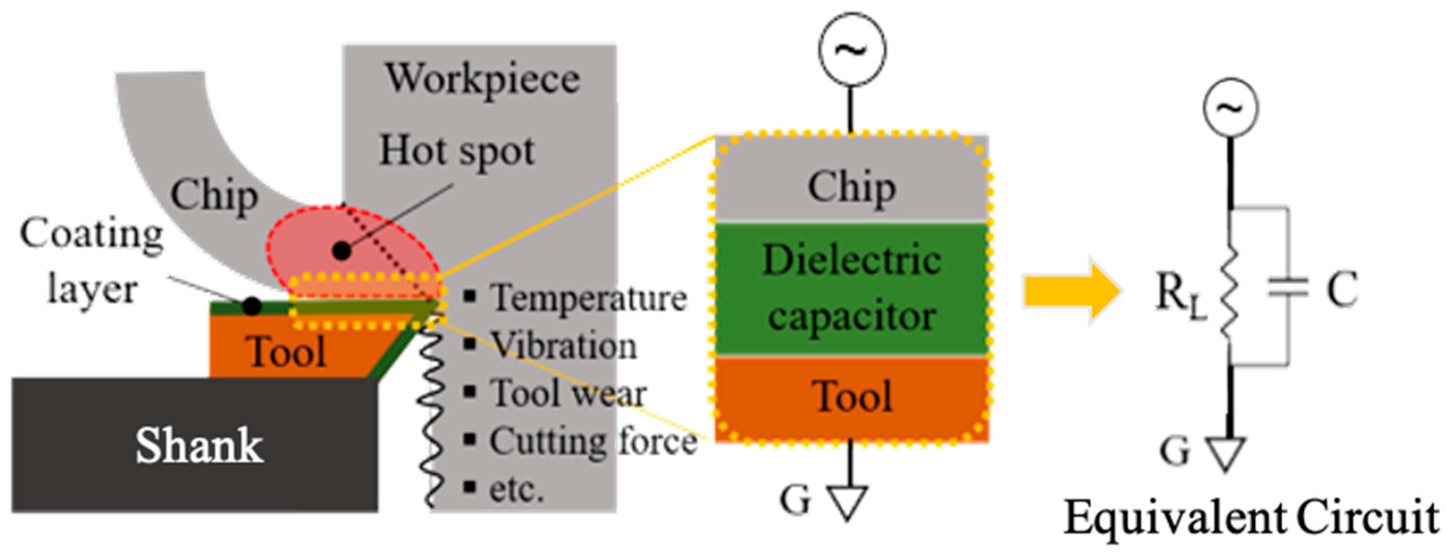
2. Methodology
3. Validation
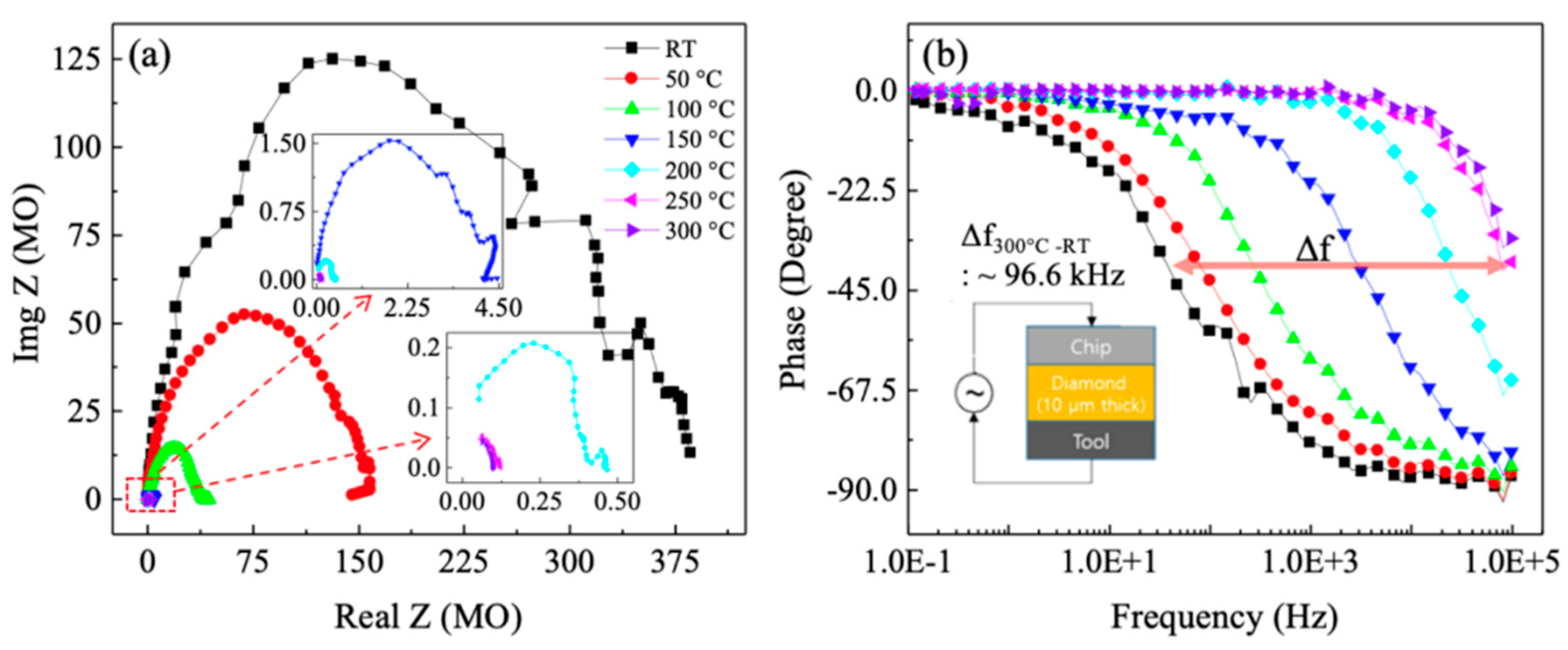
Impedance Spectroscopy
4. Experiments and Results
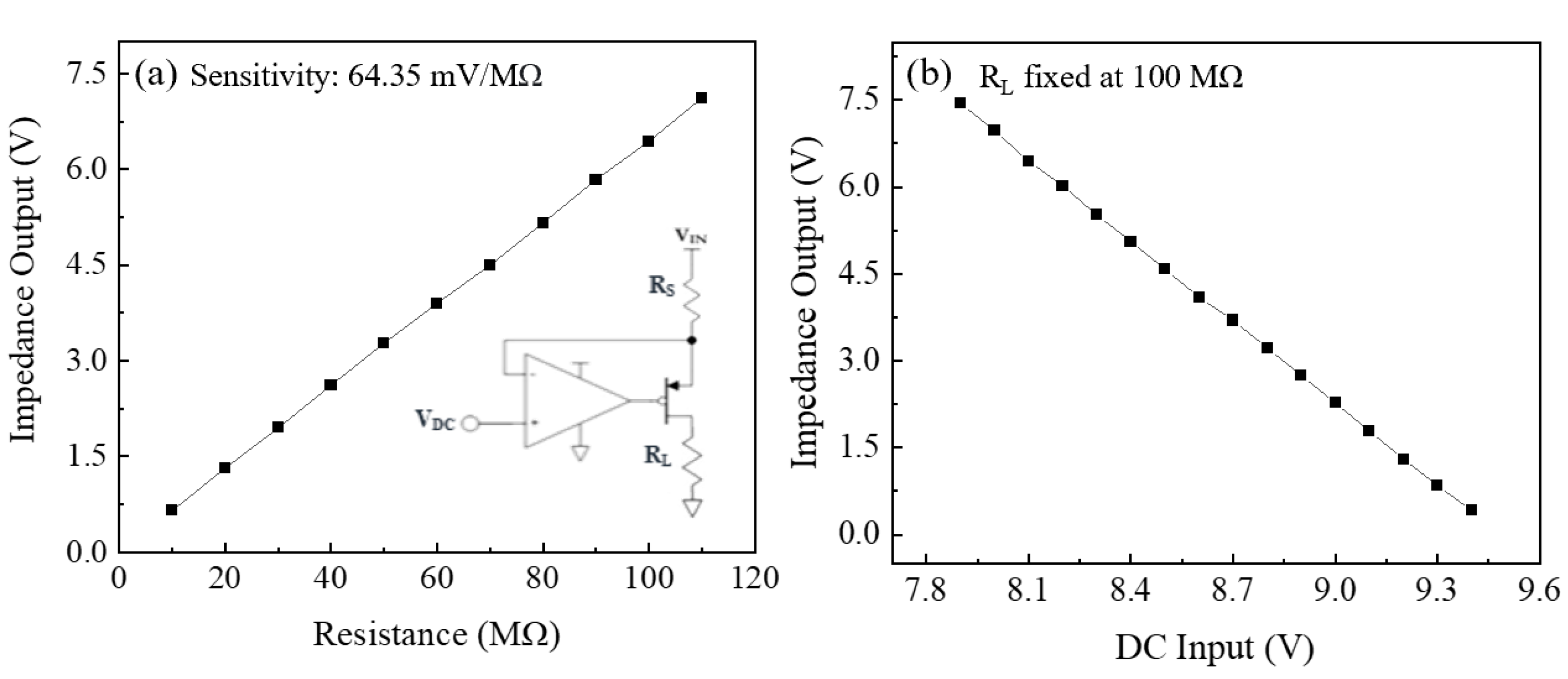
4.1. Voltage Controlled Current Source (VCCS)
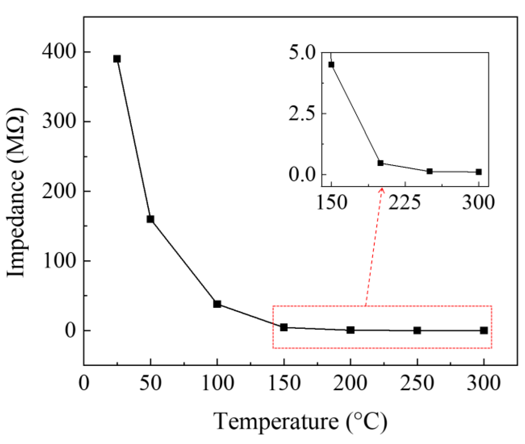
4.2. Impedance vs. Temperature
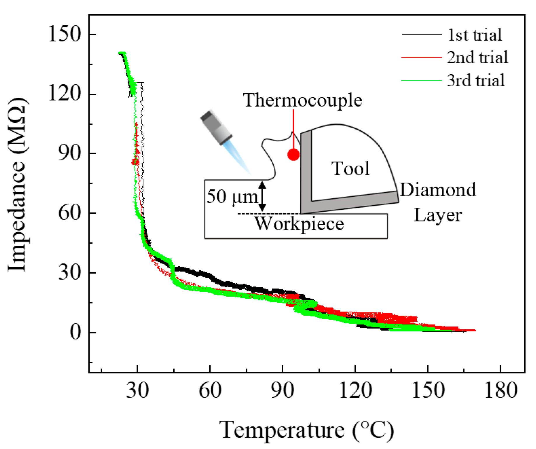
4.3. Stability Test
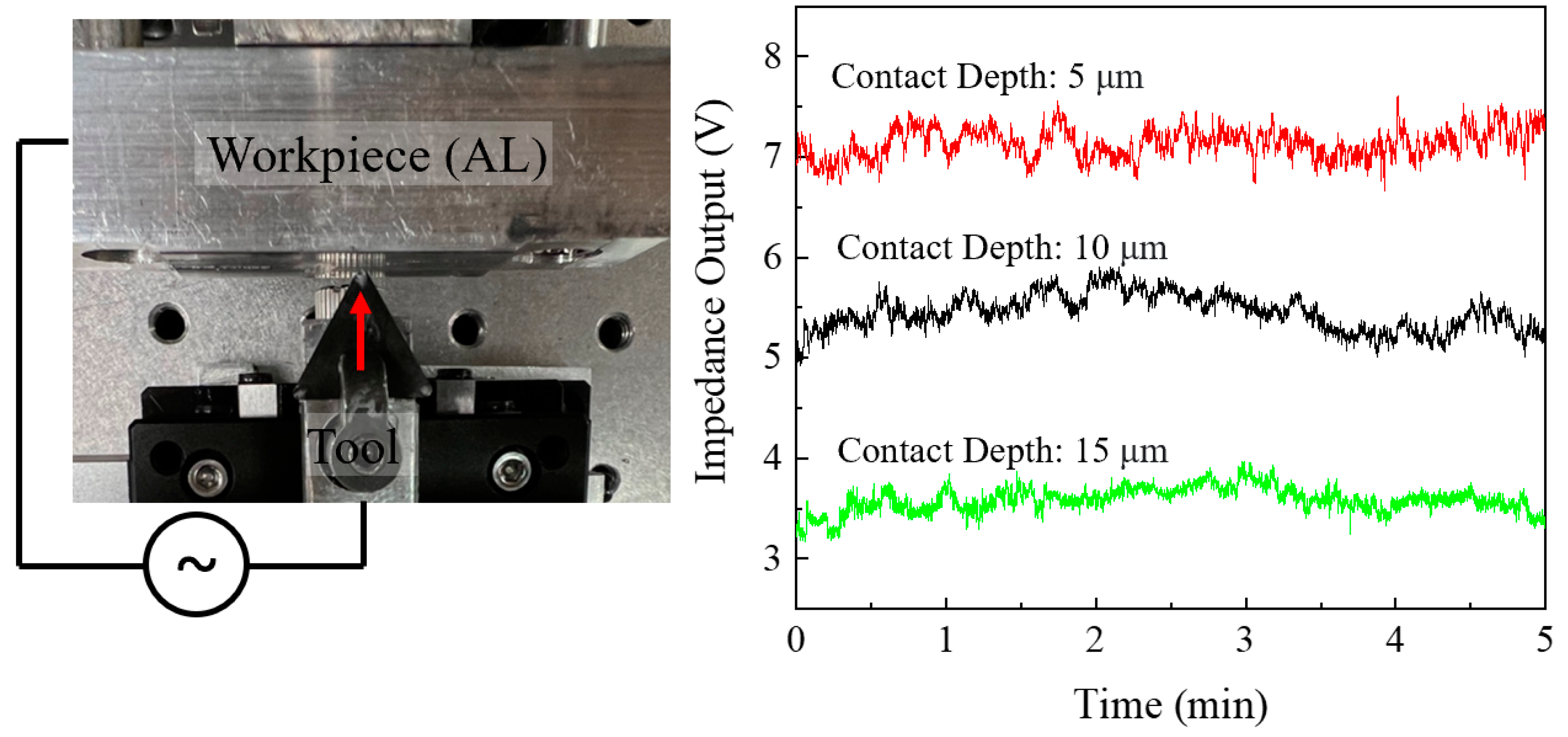
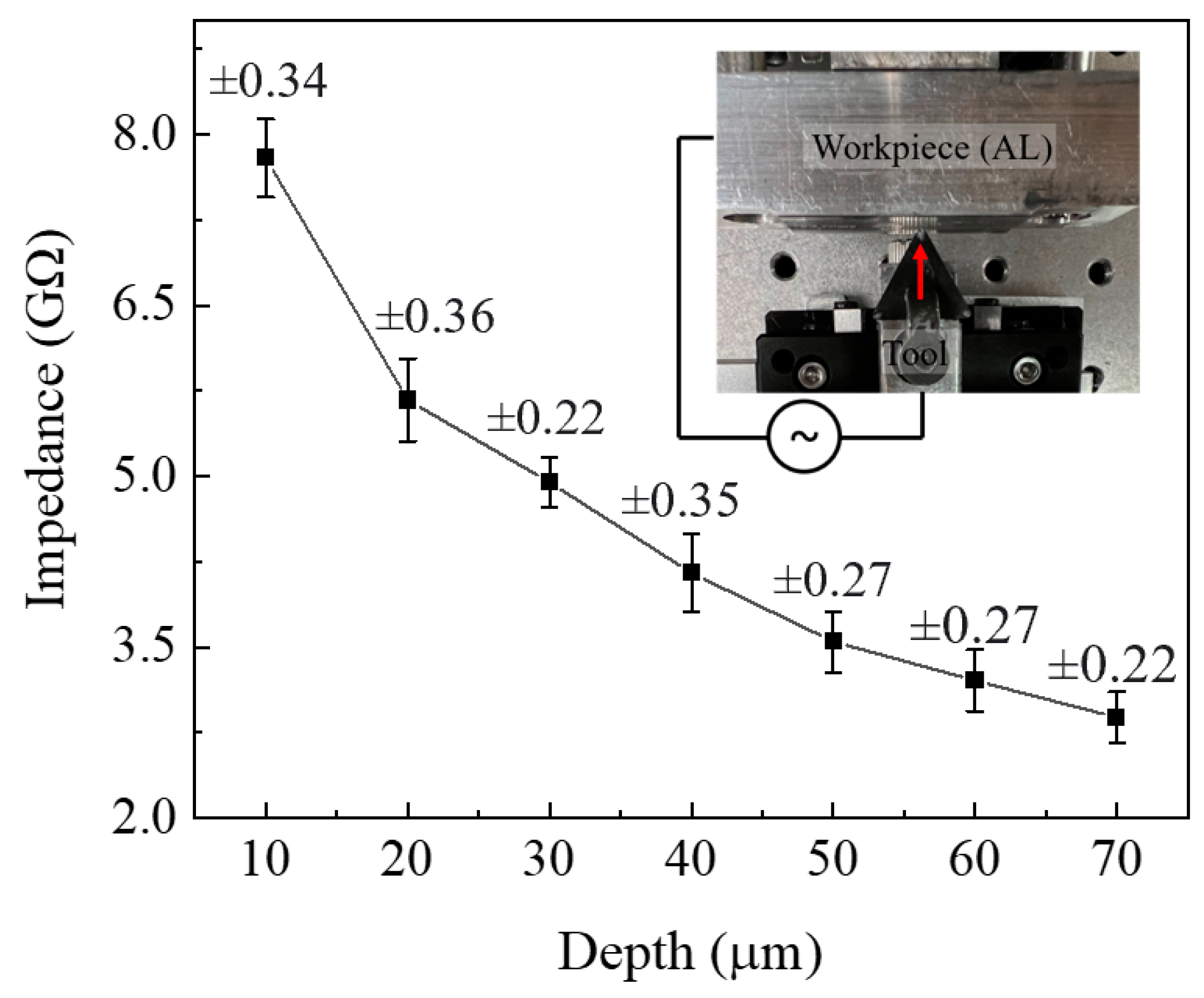
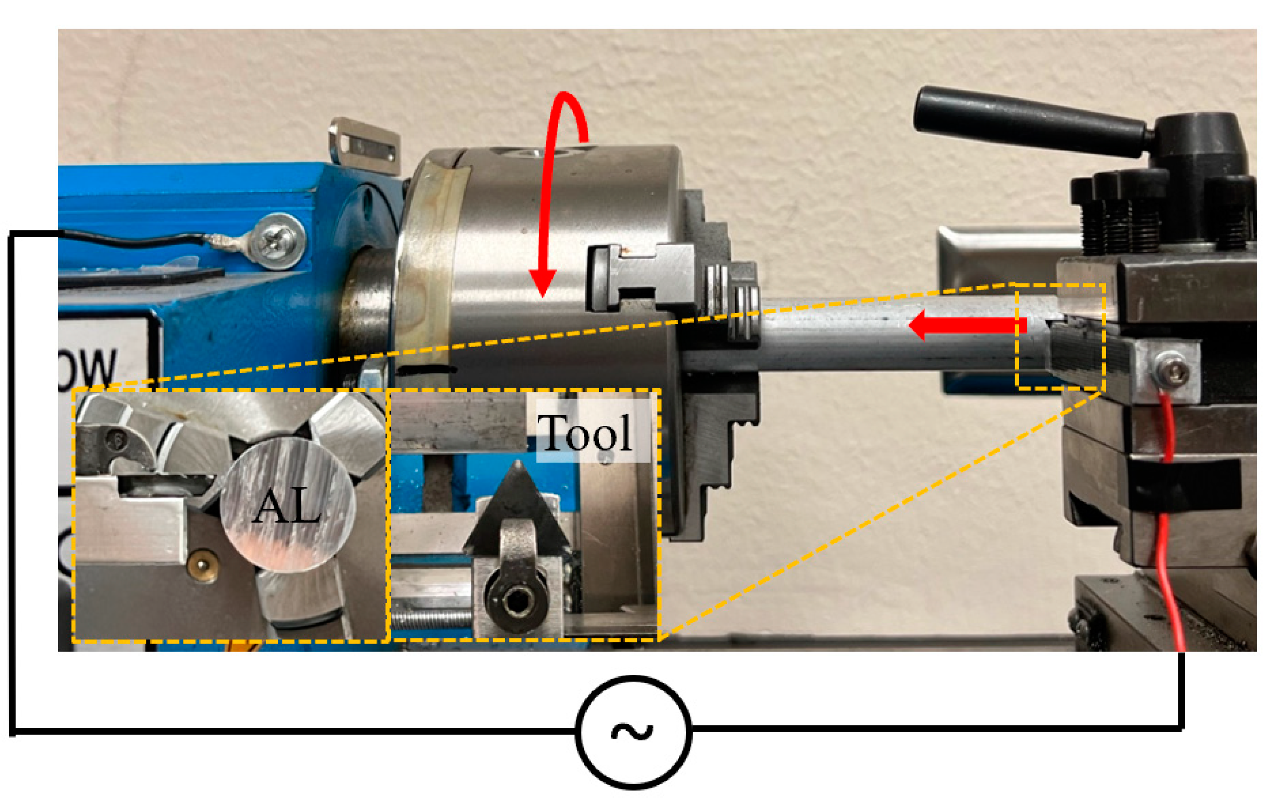
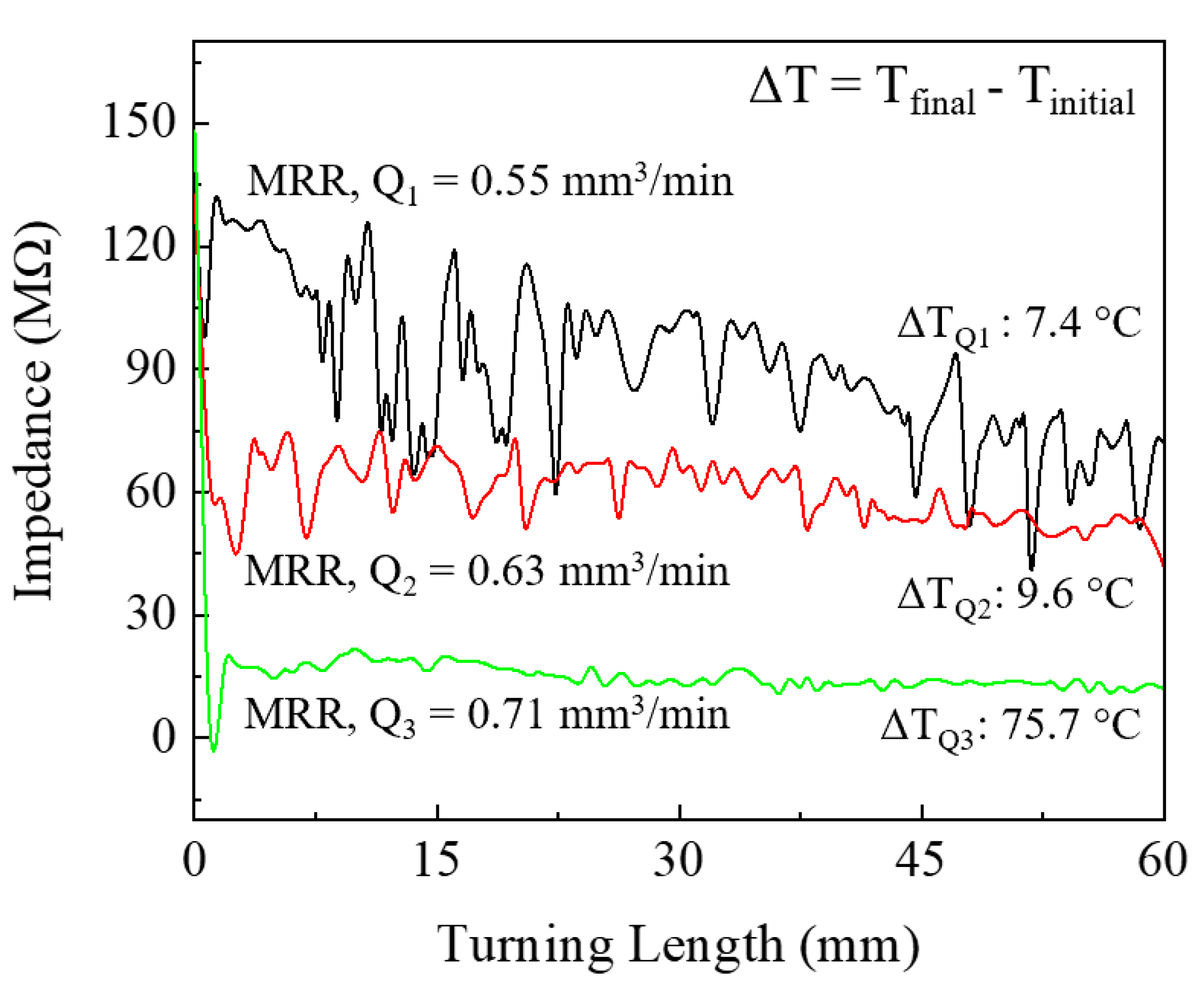
4.4. Machining Experiment
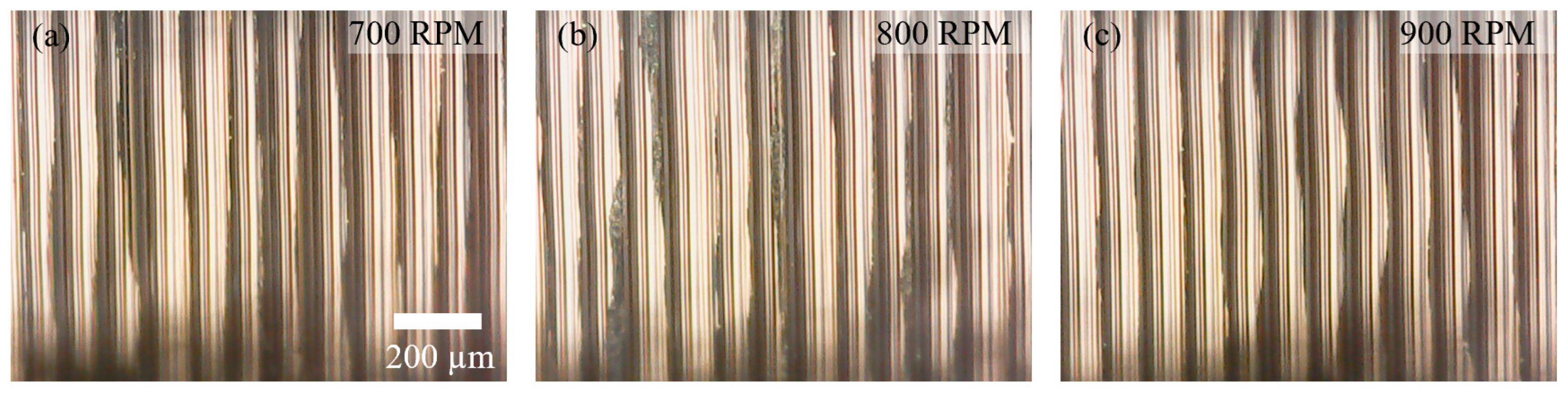
4.5. Potential Application for Indentation
5. Future Works
6. Conclusions
Author Contributions
Funding
Institutional Review Board Statement
Informed Consent Statement
Data Availability Statement
Acknowledgments
Conflicts of Interest
References
- Patel, A.J.; Kilic, G.A. A Review on Advanced Manufacturing Techniques and Their Applications; IntechOpen: Online, 2021. [Google Scholar]
- Gregório, A.V.L.; Silva, T.E.F.; Reis, A.P.; de Jesus, A.M.P.; Rosa, P.A.R. A Methodology for Tribo-Mechanical Characterization of Metallic Alloys under Extreme Loading and Temperature Conditions Typical of Metal Cutting Processes. J. Manuf. Mater. Process. 2022, 6, 46. [Google Scholar] [CrossRef]
- Ito, Y.; Kita, Y.; Fukuhara, Y.; Nomura, M.; Sasahara, H. Development of In-Process Temperature Measurement of Grinding Surface with an Infrared Thermometer. J. Manuf. Mater. Process. 2022, 6, 44. [Google Scholar] [CrossRef]
- Lee, Y.J.; Shen, Y.-K.; Wang, H. Suppression of Polycrystalline Diamond Tool Wear with Mechanochemical Effects in Micromachining of Ferrous Metal. J. Manuf. Mater. Process. 2020, 4, 81. [Google Scholar] [CrossRef]
- Knight, W.A.; Boothroyd, G. Fundamentals of Machining and Machine Tools, 3rd ed.; CRC Press: Boca Raton, FL, USA, 2005. [Google Scholar]
- Grzesik, W. Advanced Machining Processes of Metallic Materials; Elsevier: Amsterdam, The Netherlands, 2008. [Google Scholar]
- Taylor, F.W. On the Art of Cutting Metals; American Society of Mechanical Engineers: New York, NY, USA, 1907. [Google Scholar]
- Trent, E.M.; Wright, P.K. Metal Cutting, 4th ed.; Butterworth–Heinemann: Boston, MA, USA, 2000; 446p. [Google Scholar]
- Carvalho, S.R.; e Silva, S.L.; Machado, A.R.; Guimaraes, G. Temperature determination at the chip–tool interface using an inverse thermal model considering the tool and tool holder. J. Mater. Process. Technol. 2006, 179, 97–104. [Google Scholar] [CrossRef]
- Rodríguez, J.M.; Jonsén, P.; Svoboda, A. Simulation of metal cutting using the particle finite-element method and a physically based plasticity model. Comput. Part. Mech. 2017, 4, 35–51. [Google Scholar] [CrossRef]
- Lazoglu, I.; Altintas, Y. Prediction of tool and chip temperature in continuous and interrupted machining. Int. J. Mach. Tools Manuf. 2002, 42, 1011–1022. [Google Scholar] [CrossRef]
- Kesriklioglu, S.; Arthur, C.; Morrow, J.D.; Pfefferkorn, F.E. Characterization of Tool–Chip Interface Temperature Measurement With Thermocouple Fabricated Directly on the Rake Face. ASME. J. Manuf. Sci. Eng. 2019, 141, 091008. [Google Scholar] [CrossRef]
- Sutter, G.; Fauré, L.; Molinari, A.; Ranc, N.; Pina, V. An experimental technique for the measurement of temperature fields for the orthogonal cutting in high speed machining. Int. J. Mach. Tools Manuf. 2003, 43, 671–678. [Google Scholar] [CrossRef]
- Kesriklioglu, S.; Morrow, J.D.; Pfefferkorn, F.E. Tool–Chip Interface Temperature Measurement in Interrupted and Continuous Oblique Cutting. ASME. J. Manuf. Sci. Eng. 2018, 140, 051013. [Google Scholar] [CrossRef]
- Attia, M.H.; Cameron, A.; Kops, L. Distortion in Thermal Field around Inserted Thermocouples in Experimental Interfacial Studies, Part 4: End Effect. J. Manuf. Sci. Eng. 2002, 124, 135–145. [Google Scholar] [CrossRef]
- Davies, M.A.; Ueda, T.; Saoubi, R.M.; Mullany, B.; Cooke, A.L. On the measurement of temperature in material removal processes. Ann. CIRP 2007, 56, 581–604. [Google Scholar] [CrossRef]
- Woodbury, A. Effect of deterministic thermocouple errors on the solution of the inverse heat conduction problem. In Proceedings of the 5th International Conference on Inverse Problems in Engineering: Theory and Practice, Cambridge, UK, 11–15 July 2005. [Google Scholar]
- Abhang, L.B.; Hameedullah, M. The Measurement of chip-tool interface temperature in the turning of steel. Int. J. Comput. Commun. Inf. Syst. (IJCCIS) 2010, 2, 1–5. [Google Scholar]
- Kus, A.; Isik, Y.; Cakir, M.C.; Coşkun, S.; Özdemir, K. Thermocouple and Infrared Sensor-Based Measurement of Temperature Distribution in Metal Cutting. Sensors 2015, 15, 1274–1291. [Google Scholar] [CrossRef]
- Jeelani, S. Measurement of temperature distribution in machining using IR photography. Wear 1981, 68, 191–202. [Google Scholar] [CrossRef]
- Boothroyd, G. Photographic technique for the determination of metal cutting temperatures. Br. J. Appl. Phys. 1961, 12, 238–242. [Google Scholar] [CrossRef]
- Longbottom, J.M.; Lanham, J.D. Cutting temperature measurement while machining—A review. Aircr. Eng. Aerosp. Technol. 2005, 77, 122–130. [Google Scholar] [CrossRef]
- Lin, J.; Liu, C. Measurement of Cutting Tool Temperature by an Infrared Pyrometer. Meas. Sci. Technol. 2001, 12, 1243–1249. [Google Scholar] [CrossRef]
- Lin, J.; Lee, S.; Weng, C. Estimation of Cutting Temperature in High Speed Machining. ASME. J. Eng. Mater. Technol. 1992, 114, 289–296. [Google Scholar] [CrossRef]
- Storchak, M.; Stehle, T.; Möhring, H.C. Determination of thermal material properties for the numerical simulation of cutting processes. Int. J. Adv. Manuf. Technol. 2022, 118, 1941–1956. [Google Scholar] [CrossRef]
- Akbar, F.; Mativenga, P.T.; Sheikh, M.A. An Investigation of the Tool-Chip Interface Temperature and Heat Partition in High-speed Machining of AISI/SAE 4140 Steel with TiN-coated Tool. In Proceedings of the 35th International MATADOR Conference, Taipei, Taiwan, July 2007; Hinduja, S., Fan, K.C., Eds.; Springer: London, UK, 2007. [Google Scholar]
- Karner, J.; Pedrazzini, M.; Reineck, I.; Sjostrand, M.E.; Bergmann, E. CVD diamond coated cemented carbide cutting tools. Mater. Sci. Eng. A 1996, 209, 405–413. [Google Scholar] [CrossRef]
- Ebert, W.; Adamschik, M.; Gluche, P.; Flöter, A.; Kohn, E. High-temperature diamond capacitor. Diam. Relat. Mater. 1999, 8, 1875–1877. [Google Scholar] [CrossRef]
- Lanfredi, S. Impedance spectroscopy study of the electrical conductivity and dielectric constant of polycrystalline LiNbO3. J. Appl. Phys. 1999, 86, 2215. [Google Scholar] [CrossRef]
- Radtke, M.; Hess, C. Easy-Made Setup for High-Temperature (Up to 1100 °C) Electrochemical Impedance Spectroscopy. J. Mater. Eng. Perform. 2022. [Google Scholar] [CrossRef]
- Bachrathy, D.; Kiss, A.K.; Kossa, A.; Berezvai, S.; Hajdu, D.; Stepan, G. In-Process Monitoring of Changing Dynamics of a Thin-Walled Component During Milling Operation by Ball Shooter Excitation. J. Manuf. Mater. Process. 2020, 4, 78. [Google Scholar] [CrossRef]
- Ganesan, D.; Sellamuthu, P.; Prashanth, K.G. Vacuum Hot Pressing of Oxide Dispersion Strengthened Ferritic Stainless Steels: Effect of Al Addition on the Microstructure and Properties. J. Manuf. Mater. Process. 2020, 4, 93. [Google Scholar] [CrossRef]
- Langenhorst, L.; Sölter, J.; Kuschel, S. Partition of Primary Shear Plane Heat in Orthogonal Metal Cutting. J. Manuf. Mater. Process. 2020, 4, 82. [Google Scholar] [CrossRef]


| Temperature (°C) | RT | 50 | 100 | 150 | 200 | 250 | 300 |
| Capacitance (pF) | 8.8 | 10.2 | 13.4 | 7.7 | 11.1 | 13.5 | 14.5 |
Publisher’s Note: MDPI stays neutral with regard to jurisdictional claims in published maps and institutional affiliations. |
© 2022 by the authors. Licensee MDPI, Basel, Switzerland. This article is an open access article distributed under the terms and conditions of the Creative Commons Attribution (CC BY) license (https://creativecommons.org/licenses/by/4.0/).
Share and Cite
Chun, H.; Park, W.; Kim, J.; Lee, C. In-Process Cutting Temperature Monitoring Method Based on Impedance Model of Dielectric Coating Layer at Tool-Chip Interface. J. Manuf. Mater. Process. 2022, 6, 97. https://doi.org/10.3390/jmmp6050097
Chun H, Park W, Kim J, Lee C. In-Process Cutting Temperature Monitoring Method Based on Impedance Model of Dielectric Coating Layer at Tool-Chip Interface. Journal of Manufacturing and Materials Processing. 2022; 6(5):97. https://doi.org/10.3390/jmmp6050097
Chicago/Turabian StyleChun, Heebum, William Park, Jungsub Kim, and ChaBum Lee. 2022. "In-Process Cutting Temperature Monitoring Method Based on Impedance Model of Dielectric Coating Layer at Tool-Chip Interface" Journal of Manufacturing and Materials Processing 6, no. 5: 97. https://doi.org/10.3390/jmmp6050097
APA StyleChun, H., Park, W., Kim, J., & Lee, C. (2022). In-Process Cutting Temperature Monitoring Method Based on Impedance Model of Dielectric Coating Layer at Tool-Chip Interface. Journal of Manufacturing and Materials Processing, 6(5), 97. https://doi.org/10.3390/jmmp6050097