Abstract
A drastically growing requirement of electronic packages with an increasing level of complexity poses newer challenges for the competitive manufacturing industry. Coupled with harsher operating conditions, these challenges affirm the need for encapsulated board-level (2nd level) packages. To reduce thermo-mechanical loads induced on the electronic components during operating cycles, a conformal type of encapsulation is gaining preference over conventional glob-tops or resin casting types. The availability of technology, the ease of automation, and the uncomplicated storage of raw material intensifies the implementation of thermoset injection molding for the encapsulation process of board-level packages. Reliability case studies of such encapsulated electronic components as a part of board-level packages become, thereupon, necessary. This paper presents the reliability study of exemplary electronic components, surface-mounted on printed circuit boards (PCBs), encapsulated by the means of thermoset injection molding, and subjected to cyclic thermal loading. The characteristic lifetime of the electronic components is statistically calculated after assessing the probability plots and presented consequently. A few points of conclusion are summarized, and the future scope is discussed at the end.
Keywords:
encapsulation; board level package; electronics; epoxy molding compound; flow simulation; injection molding; injection molding simulation; lifetime; manufacturing; PCB; QFN; reliability; resistors; SMD; surface mount technology; thermoset; transfer molding; Weibull; boxplot; capacitor; CTE; material processing; mold trials; scanning acoustic microscopy; temperature shock 1. Introduction
The recently changing trends in the automotive sector towards greener and autonomous mobility and the ever increasing growth in the market of handheld devices (especially towards 5G implementation) coupled with other consumer dominant markets enforce the electronics industry to constantly improve itself in terms of functional integration and miniaturization with minimum compromise on the reliability. To attain a certain level of functional integration and miniaturization, the need of board-level (2nd level) packages crops up. The robustness, namely the ability of the package to protect itself from external harmful media and withstand or overcome adverse environmental conditions, is brought in by means of a board-level encapsulation.
An assessment of thermoset injection molding for the encapsulation of PCBs with surface-mounted electronic components was presented in a previous work [1]. During that assessment, mold trials were carried out as a part of a chalked out design of experiments (DoE) with PCBs of different transition temperatures (125 °C and 170 °C) and different encapsulation thicknesses (0.25 to 1 mm) to evaluate the implementation of thermoset injection molding as an alternative to other dominant methods for the purpose of the encapsulation of board-level packages. An example of such an encapsulated package is shown in Figure 1. The definition of levels of packaging (here, 2nd level package) is taken from [2] and was also summarized in [1]. As mentioned already in [1], extensive literature is not available on this particular topic (encapsulation of 2nd level packages with the help if thermoset injection molding). Extensive research is, however, available in the field of 1st level packaging with encapsulations manufactured by transfer molding [3,4] and as a part of the Cornell injection molding program (CIMP), especially report 16 [5]. Further literature is also available relating to wafer-level encapsulations [6,7,8,9]. An approach for the reliability analysis can be derived according to a standard operating procedure used for microsystem technology in the automotive sector, as also used in [10]. This procedure is explained in the Section 2.4 and Section 2.5. Useful tips and relevant information about board-level reliability of different components (without 2nd level encapsulation) are available in different sources [11,12,13,14,15,16,17,18,19]. These sources lay out the best practices used for defining and testing board-level reliability, involving the reliability analysis of commonly used components like ball grid arrays (BGAs) [13,16], quad-flat no-leads packages (QFN) [11,15], and thin small outline packages [17]. The effect of 2nd level encapsulation, e.g., by means of conformal potting on QFN reliability is presented in [20]. The fundamentals (distribution and probability) and definitions regarding lifetime and reliability are taken from [21], leading to the choice of valid analysis methods dependent on case information. This systematic approach for the reliability analysis is followed in line with a previous work [22], which presents the reliability analysis of different commonly used electronic components (ceramic resistors, BGAs, QFN, and small outline packages) mounted on different substrates relevant for molded interconnect devices (MID).
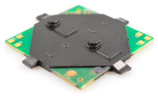
Figure 1.
Example of encapsulated board-level packages as an outcome of earlier mold trials [1].
In the sections to follow, the conception of such a package to be encapsulated is introduced (Section 2.1), a filling process simulation is presented (Section 2.2), the executed mold trials are detailed out (Section 2.3) before the test-setup is exhibited (Section 2.4) and the implementation of the tests is explained (Section 2.5). Furthermore, the mechanisms of the failure of the components are evaluated (Section 3.1) and the statistical analysis of the recorded data is put forth (Section 3.2). In the end, the results are discussed along with the drawn conclusions (Section 4).
2. Materials and Methods
2.1. Conception of the Package
A board-level package with commonly used electronic components was designed. Some of these components and the package with the mounted components are shown in Figure 2. The chosen and mounted components are enlisted in Table 1. A printed circuit board (PCB) of size 55 mm × 55 mm × 1.55 mm was used. To avoid the bending of the PCB during the overmolding process, as noticed in [1], boards made of a material with a high glass transition temperature (170 °C) were procured. A thermo-mechanical analysis (TMA) was carried out on a sample to confirm the transition temperature. The PCBs were subsequently subjected to a 100% inspection process for electrical connectivity of all the mounted components.
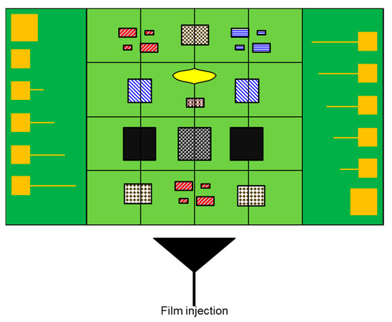
Figure 2.
Conception of the electronic assembly to be encapsulated. It involves a wide range of applied surface-mounted components. See legend in Table 1.

Table 1.
List of mounted electronic components on each printed circuit board (PCB).
The encapsulation was carried out using the thermoset injection molding process. For this purpose, an Arburg Allrounder 375 V with necessary attachments, tooling, and encapsulation material (NU6110V by Duresco) analog to [1] was used. The chosen material is easily available in the European market and, according to the manufacturer, is suitable for this purpose. The fed granulate of the material was heated at a temperature of 70 °C and then injected into a molding tool held at elevated temperatures of 160 to 175 °C, which contained the mounted PCB as a mold insert.
2.2. Process Simulation
To reduce the risks of defects during the injection molding process and to optimize the tempering concept, a simulation study using SIGMASOFT® was carried out beforehand. The geometry model used for these simulations can be seen in Figure A1 (Appendix A). Process parameters such as melt temperature, tool temperature, flow control, etc., are fed to the simulation with reference to material data [23] and based on previous experience. These parameters are listed in Table 2.
Table 2.
Process parameters for the injection molding simulation.
The output of the simulation can be seen in Figure 3. The material manufacturer recommends (which is also confirmed by earlier experience gained during [1]) that a sprue (runner) length of approximately 100 mm is required for the processed material to attain a temperature of around 130 °C. The simulation showed that such a temperature level could be realized in this case successfully. Six filling stages are shown with an indicated percentage of cavity filled. The total cavity volume is defined as the encapsulation and the runner system together. As seen in the stage 50% filled, it can be noted that the runner system contributes to a little more than half of the cavity to be filled to ensure that a higher melt temperature is attained—a temperature level required to achieve the low viscosity of flowing melt and subsequently accelerate the curing after the filling stage is complete. A video of the filling simulation is made available as Supplementary Materials to this article.
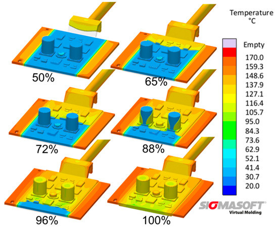
Figure 3.
Series of filling behavior (with the % of cavity filled including the runner system) during the simulated injection molding process. The simulation shows a near to uniform filling behavior with a sufficiently attained melt temperature (~130 °C).
2.3. Mold Trials
The mold trials were carried out in a sequential manner according to the experience gained during the earlier feasibility tests. Regular purging and cleaning of the molding tool, as per the recommendations of the material and machine suppliers, were carried out before, during, and after the mold trials. The process parameters had to be fine-tuned as per the interim molding results. The final parameters are listed out in Appendix A (Table A1 and Table A2).
As a standard practice, a mold filling study was conducted to measure and adjust the injection screw speeds and time intervals. This filling study also serves to observe the filling behavior of the melt in the mold cavity and to compare the same with the process simulation results. After conducting several mold (pilot) trials, an optimized filling pattern was achieved and is presented in Figure 4. The upper row of pictures shows the flow pattern on the (surface)-mounted side of the PCB and the lower row shows the same on the unmounted side. The real flow pattern is similar to the pattern foreseen by means of the process simulation (Figure 3).
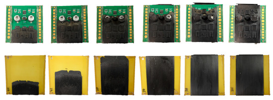
Figure 4.
Results of mold trials. The upper row shows the front (mounted) side, and the lower row shows the hind (unmounted) side.
2.4. Test Setup
Eight packages of each of the two types, namely open and encapsulated, were electrically tested, soldered with connecting cables, and then fixed on two mounting plates (one mounting plate shown in Figure 5). All the mounted components on the PCBs with connecting pads on the left side were connected for inline testing by means of resistance measurement. The components that led to the right side of the PCB were the thermistor and the capacitors which were not tested inline. The capacitors were tested for functionality after definite relevant intervals.
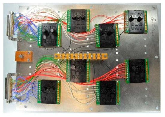
Figure 5.
Eight encapsulated PCBs fixed on the mounting plate to be placed in the climatic chamber for the temperature shock tests.
2.5. Running of Tests
The two mounting plates were placed in the climatic chamber (CTS TSS-70/130) for the thermal shock tests. The test conditions were defined according to current advancements and other standard practices in the automotive industry. The packages were subjected to thermal cyclic loading (shock), involving temperature levels of +150 °C and −40 °C with a holding time of 15 min on each side. Apart from the chamber changing time of 10 s, a waiting time of 60 s was induced before measuring the resistance at each temperature level to allow for the thermal equilibrium of the system. The adequacy of this waiting time was checked by means of thermistor measurements on sample packages. Figure 6 shows the process flow for a systematic approach towards reliability analysis, which was followed and can also be applied to analyze similar parts or components.
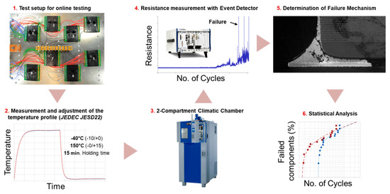
Figure 6.
Systematic approach for the climatic tests for reliability analysis showing the illustrative images of each stage.
3. Results
3.1. Mechanisms of Failure
To investigate the different mechanisms of failure for the packages and the individual mounted components, these were subjected to multiple tests. Firstly, visual inspection was carried out to notice abnormalities on the packages, e.g., missing components from open packages and surface of the encapsulation. Open PCBs witnessed the falling off of failed components due to the failure of the solder joint. In some cases, the encapsulation suffered from cracks due to the thermal shock loading.
The next stage of tests involved the use of a scanning acoustic microscope to investigate the interface between the encapsulation and the PCB. Figure 7 shows a widespread delamination of the encapsulation from the PCB, owing to the thermal cyclic loading and different coefficients of thermal expansion (CTE mismatch). Cracks in the encapsulation can also be noted in this image. In the current example, this crack is positioned in the flow shadow region of the ElKo. This region poses itself as a strong candidate for the building of a weld line during injection molding (Figure 3 and Figure 4).
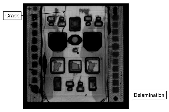
Figure 7.
Image from scanning acoustic microscopy showing widespread delamination after long term thermal cyclic loading.
The packages were then subjected to X-Ray solder joint inspection. The solder joints had failed, not sustaining the extensive thermal shock environment. Figure 8 shows examples of the components under the encapsulation with initiated or complete cracks through the solder joints.
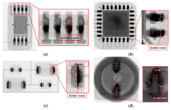
Figure 8.
Images from the X-ray microscopy carried out on the different components on the PCB after the end of the thermal cyclic tests: (a) TSSOP8 and (b) MLF28 show solder cracks, whereas (c) the resistors and (d) ElKo show a combination of solder cracks and pores.
A selection of these components was randomly chosen to be further subjected to a more extensive optical microscopy after the preparation of relevant cross-sections. Figure 9 shows examples of the output of the microscopic analysis.
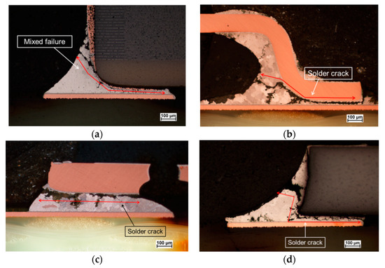
Figure 9.
Images showing the failed solder joints of different components: (a) a mixed mechanism of failure of a ceramic capacitor, and cracks in the solder joints of (b) TSSOP, (c) MLF28, and (d) CR1206.
3.2. Statistical Analysis of Reliability
A boxplot study (Figure 10) was first carried out to identify and rule out statistical outliers based on the number of sustained cycles. A reference censoring (time) was made at 9147 cycles since the tests were ceased at this point (<5% of the components were still running).
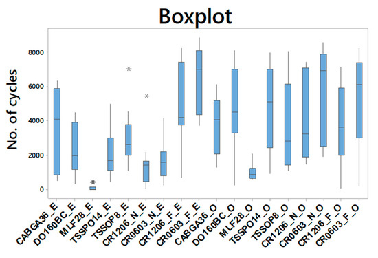
Figure 10.
Boxplot analysis showing statistical outliers marked with asterisks. The outliers were not considered in further analysis. The component nomenclature is defined in Table 1.
The further analysis was based on two main categories of the tested parts, namely open and encapsulated packages. For ease of representation, shorter forms of the component names were used (as mentioned in Table 1). The suffix “E” was used for components on encapsulated probes and the suffix “O” was used for components, which were not encapsulated. Since two sets of chip resistors were mounted on the PCBs, they were identified by means of “N” for near sprue and “F” for far away from sprue.
According to [24], Weibull (3 parameters) was the preferred method of distribution analysis considering the following reasons:
- The correlation coefficient should be greater than for the second-best distribution.
- The data in the Weibull plot indicate a curvature (concave curve).
- A large sample size (n > 20) is available; with previous knowledge of a time without failure, eight to ten must be sufficient.
- A physical explanation of why a failure-free can occur.
The distribution analysis was carried out with the help of probability plots involving different analysis methods. A comparison of the correlation coefficients for the methods was carried out. A comparison of all the correlation coefficients is shown in the Appendix A (Table A3). The Weibull (3 parameter) distribution came out to provide the best fit for most of the plots (15 out of 18) and indicated a concave curvature. Since previous knowledge of the failure of similar components is available through an earlier project [22], a sample size of at least eight was deemed sufficient. The encapsulated parts were subjected to a tempering (curing) process at 160 °C for 3 h, then all the PCBs, open and encapsulated, were electrically tested before being subjected to thermal shock tests. This rules out the existence of weak (defective) specimen in the chosen test samples. The characteristic lifetime (63.2% parts failed) was deduced from this distribution analysis using the least squares estimation method for each constellation according to [21,25].
Looking at Figure 11, it was noticed, in general, that the encapsulation reduces the characteristic lifetime of the mounted components except in the forth-mentioned cases. Encapsulated BGAs witness no significant change (<2%) in the lifetime as compared to the corresponding open BGAs. The resistors in the area far from the sprue also showed a peculiar behavior. The encapsulated CR0603 resistors in this zone (far) showed only a slight fall (<3%) in the lifetime, whereas the encapsulated CR1206 resistors exhibited a gain (22%) in the lifetime as compared to their counterparts on the open PCBs. This can possibly be attributed to the longer flow length that the material in this zone (far) has to undergo, which provides scope for earlier cross-linking of the encapsulation. Moreover, the components in the zone near the sprue are subjected to higher glass fiber concentration in the encapsulation induced during the packing/curing phase.
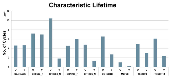
Figure 11.
Histogram showing the deduced characteristic lifetime values for all the combinations. The component nomenclature is defined in Table 1.
Figure 12 shows two chosen cases of comparison, the best and the worst case, as examples with maximum difference in the characteristic lifetime in the positive and negative directions. The diagram on the left (a) shows the case of the resistors CR1206 placed in the zone far away from the injection sprue. This combination experiences a rise in the characteristic lifetime after encapsulation by approximately 22% in comparison to their open counterparts. On the right side (b), the example of MLF28 is shown, which shows, as the worst case, a drop in the characteristic lifetime by approximately 80%. The components MLF are already known to have the least lifetime compared to other components according to [22]. Moreover, they have a very thin gap of less than 100 µm under them till the PCB, which allows only the polymer matrix of the epoxy molding compound (EMC) to enter. This matrix usually has a higher CTE compared to the glass-filled EMC.
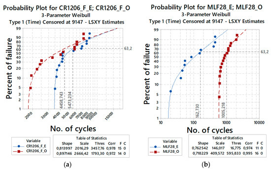
Figure 12.
Probability plots according to the least squares’ estimation method and right censored data at 9147 cycles, showing the combinations with the maximum differences in lifetime. (a) The maximum gain in case of CR1206_F and (b) the maximum reduction in case of MLF28.
The capacitors were not tested online due to the limitation of the measurement equipment to only monitor electric resistance values. These components were present on the PCB as part of a feasibility study only. They were, however, checked for electric contact and capacitance values after 50, 100, 250, 500, and thereafter at regular intervals of 500 cycles though they were not the focus during this reliability study. All the electrolytic capacitors (open and encapsulated) were reported to have failed by 6000 cycles. By 7500 cycles, all the encapsulated capacitors (ceramic and electrolytic) were announced as failed owing to either missing contact or minimal residual capacitance.
4. Discussion and Conclusions
Conclusions were drawn through the various stages in this study. The implementation of the thermoset injection molding on an industry-relevant package was successfully carried out based on earlier feasibility analysis. The filling velocity had to be adjusted in a way that the lower viscosity of the melt was reached in a suitable time that enabled the filling of not only the cavities around the ElKo (e-caps) but also produced a well filled tail end of the encapsulation on the PCB.
After the environmental tests, it was derived through X-Ray analysis that solder joint cracking is the most often occurring mechanism of failure for components encapsulated using thermoset injection molding. This was further confirmed by virtue of cross-sectional analysis. This failure of the components is attributed to various stages of CTE mismatch through the encapsulation material, FR4, metallization, the solder joint, and the component. Delamination also occurs at the interface of the encapsulation and the PCB by virtue of CTE mismatch during the thermal cyclic loading. The encapsulation also experiences cracking subsequently.
The characteristic lifetime of the resistors CR1206 increases in the zone away from sprue with the presence of the 0.5-mm-thick encapsulation. The BGAs witness insignificant change in the characteristic lifetime with thermoset injection molded encapsulation. The characteristic lifetime of the rest of the components reduces with different proportions due to the 0.5-mm-thick encapsulation. The location of a component over the PCB (near or far from the sprue location) is seen to play a vital role in the change of the characteristic lifetime. A strong dependency of the characteristic lifetime on the thickness of the encapsulation and the fiber orientation is also likely and is currently under scrutiny. The factors contributing to the rise and fall of the characteristic lifetime need to be provoked intentionally and investigated further. These dependencies can also be evaluated with the help of coupled simulations based on fiber orientation dependent material properties similar to previous works [22,26]. An article covering the systematic approach of such coupled simulations with detailed modelling of the solder joints is planned in the near future.
Supplementary Materials
The following are available online at https://www.mdpi.com/2504-4494/4/1/26/s1, Video S1.
Author Contributions
For research articles with several authors, a short paragraph specifying their individual contributions must be provided. The following statements should be used “conceptualization, R.K. and T.G. (Tobias Groezinger); methodology, R.K. and P.W.; software, T.G. (Tobias Groezinger); validation, R.K., M.S. and T.G. (Tobias Groezinger); formal analysis, R.K.; investigation, R.K.; resources, T.G. (Tobias Groezinger) and T.G. (Thomas Guenther); data curation, R.K.; writing—original draft preparation, R.K.; writing—review and editing, M.S. and T.G. (Tobias Groezinger); visualization, T.G. (Thomas Guenther); supervision, K.-P.F. and A.Z.; project administration, R.K.; funding acquisition, T.G. (Thomas Guenther), K.-P.F. and A.Z. All authors have read and agreed to the published version of the manuscript.
Funding
This research received no external funding.
Acknowledgments
Authors would like to thank the technical and the scientific staff at Hahn-Schickard, Stuttgart and at the Institute for Microintegration at the University of Stuttgart for their constant support and motivation during the execution of this piece of research.
Conflicts of Interest
The authors declare no conflict of interest.
Appendix A

Figure A1.
Geometry Model used for the process simulation.
Table A1.
Injection molding process parameters.
Table A1.
Injection molding process parameters.
| Phase | Parameter | Unit | Phase 1 | Phase 2 | Phase 3 |
|---|---|---|---|---|---|
| Injection | Feeding volume | cm3 | 12.650 | ||
| Flow flux | cm3/s | 1 | 0.5 | 0.3 | |
| Pressure | bar | 900 | 850 | 800 | |
| Switching volume | cm3 | 6.7 | 4.5 | 1.0 | |
| Packing | Flow flux | cm3/s | 1 | ||
| Pressure | bar | 100 | 50 | 25 | |
| Duration | s | 0.10 | 29.80 | 0.10 | |
Table A2.
Injection molding auxiliary parameters.
Table A2.
Injection molding auxiliary parameters.
| Phase | Parameter | Unit | Phase 1 |
|---|---|---|---|
| Feeding | Pre-heating time | s | 30 |
| Screw speed | RPM | 80 | |
| Pressure | bar | 10 | |
| Volume | cm3 | 12.650 | |
| Decompression | Decompression flux | cm3/s | 2 |
| Decompression volume | cm3 | 0.5 | |
| Tempering | Cylinder temperature | °C | 55 |
| Nozzle temperature | °C | 70 | |
| Tool temperature up | °C | 170 | |
| Tool temperature down | °C | 170 |
Table A3.
Comparison of correlation coefficients for the fitting of the statistical data for all variants.
Table A3.
Comparison of correlation coefficients for the fitting of the statistical data for all variants.
| Distribution | CABGA36_E | DO160BC_E | MLF28_E | TSSOP14_E | TSSOP8_E | CR1206_N_E | CR0603_N_E | CR1206_F_E | CR0603_F_E | CABGA36_O | DO160BC_O | MLF28_O | TSSOP14_O | TSSOP8_O | CR1206_N_O | CR0603_N_O | CR1206_F_O | CR0603_F_O |
|---|---|---|---|---|---|---|---|---|---|---|---|---|---|---|---|---|---|---|
| Weibull | 0.899 | 0.97 | 0.947 | 0.99 | 0.991 | 0.948 | 0.966 | 0.899 | 0.954 | 0.943 | 0.895 | 0.905 | 0.948 | 0.928 | 0.943 | 0.941 | 0.951 | 0.887 |
| Lognormal | 0.936 | 0.945 | 0.967 | 0.986 | 0.985 | 0.881 | 0.941 | 0.936 | 0.942 | 0.911 | 0.843 | 0.962 | 0.901 | 0.964 | 0.965 | 0.936 | 0.958 | 0.831 |
| Loglogistic | 0.925 | 0.945 | 0.961 | 0.989 | 0.982 | 0.885 | 0.942 | 0.925 | 0.934 | 0.91 | 0.858 | 0.957 | 0.902 | 0.953 | 0.957 | 0.936 | 0.948 | 0.848 |
| 3-P Weibull | 0.978 | 0.972 | 0.974 | 0.99 | 0.994 | 0.974 | 0.969 | 0.978 | 0.959 | 0.964 | 0.989 | 0.995 | 0.974 | 0.99 | 0.983 | 0.955 | 0.972 | 0.97 |
| 3-P Lognormal | 0.959 | 0.966 | 0.971 | 0.994 | 0.992 | 0.967 | 0.972 | 0.959 | 0.955 | 0.96 | 0.987 | 0.985 | 0.962 | 0.982 | 0.972 | 0.949 | 0.959 | 0.955 |
| 3-P Loglogistic | 0.952 | 0.963 | 0.967 | 0.996 | 0.988 | 0.962 | 0.973 | 0.952 | 0.945 | 0.96 | 0.99 | 0.979 | 0.959 | 0.98 | 0.969 | 0.938 | 0.949 | 0.958 |
| Smallest Extreme Value | 0.879 | 0.939 | 0.825 | 0.901 | 0.958 | 0.965 | 0.907 | 0.879 | 0.951 | 0.964 | 0.988 | 0.835 | 0.974 | 0.859 | 0.895 | 0.939 | 0.928 | 0.97 |
| Normal | 0.928 | 0.963 | 0.89 | 0.953 | 0.988 | 0.968 | 0.952 | 0.928 | 0.955 | 0.96 | 0.987 | 0.915 | 0.962 | 0.92 | 0.941 | 0.949 | 0.959 | 0.956 |
| Logistic | 0.917 | 0.959 | 0.884 | 0.956 | 0.984 | 0.963 | 0.956 | 0.917 | 0.945 | 0.96 | 0.99 | 0.914 | 0.96 | 0.904 | 0.929 | 0.944 | 0.949 | 0.959 |
References
- Kulkarni, R.; Wappler, P.; Soltani, M.; Haybat, M.; Guenther, T.; Groezinger, T.; Zimmermann, A. An Assessment of Thermoset Injection Molding for Thin-Walled Conformal Encapsulation of Board-Level Electronic Packages. J. Manuf. Mater. Process. 2019, 3, 18. [Google Scholar] [CrossRef]
- Ardebili, H.; Zhang, J.; Pecht, M. Encapsulation Technologies for Electronic Applications; William Andrew: Oxford, UK, 2018. [Google Scholar]
- Baïri, A.; Nithyadevi, N.; Baïri, I.; Martin-Garín, A.; Millán-García, J.A. Thermal design of a sensor for building control equipped with QFN electronic devices subjected to free convection. Effects of the encapsulating resin. Energy Build. 2017, 141, 218–225. [Google Scholar] [CrossRef]
- Sasajima, H.; Watanabe, I.; Takamoto, M.; Dakede, K.; Itoh, S.; Nishitani, Y.; Tabei, J.; Mori, T. New Development Trend of Epoxy Molding Compound for Encapsulating Semiconductor Chips. In Materials for Advanced Packaging; Lu, D., Wong, C.P., Eds.; Springer International Publishing: Cham, Switzerland, 2017; pp. 373–419. ISBN 978-3-319-45098-8. [Google Scholar]
- Wang, K.; Cohen, C.; Koch, D.; Hieber, C.; Yoon, K.; Gupta, M.; Harlen, O. Cornell Injection Molding Program; Progress Report; Cornell University: Ithaca, NY, USA, 1991. [Google Scholar]
- Chih-Chung, H.; Vallury, S.; Vallury, S.; Lin, K.; Yang, A. A study on warpage behavior of EMC in post-mold cure stage using Moldex3D. Addit. Conf. (Device Packag. HiTEC HiTEN CICMT) 2016, 2016, 826–850. [Google Scholar] [CrossRef]
- Kersjes, S.H.M.; Zijl, J.L.J.; de Jong, N.; Wensink, H. Exposed Die Fan-Out Wafer Level Packaging by Transfer Molding. In Proceedings of the 2018 International Wafer Level Packaging Conference (IWLPC), San Jose, CA, USA, 23–25 October 2018; pp. 1–6. [Google Scholar]
- Kim, J.; Kim, J.; Kwon, K.-H.; Yong, Y.-S.; Kim, J.-H.; Lee, D.-H.; Kim, S.-K.; Park, D. Large Area Encapsulation: Solid Type Epoxy Molding Compound. In Proceedings of the 2018 International Wafer Level Packaging Conference (IWLPC), San Jose, CA, USA, 23–25 October 2018; pp. 1–5. [Google Scholar]
- Chiu, T.-C.; Yeh, E.-Y. Warpage simulation for the reconstituted wafer used in fan-out wafer level packaging. Microelectron. Reliab. 2018, 80, 14–23. [Google Scholar] [CrossRef]
- Müller-Fiedler, R.; Knoblauch, V. Reliability aspects of microsensors and micromechatronic actuators for automotive applications. Microelectron. Reliab. 2003, 43, 1085–1097. [Google Scholar] [CrossRef]
- Lall, P.; Deshpande, S.; Kothari, N.; Suhling, J.; Nguyen, L. Effect of Thermal Cycling on Reliability of QFN Packages. In Proceedings of the 2018 17th IEEE Intersociety Conference on Thermal and Thermomechanical Phenomena in Electronic Systems (ITherm), San Diego, CA, USA, 29 May–1 June 2018; pp. 1357–1365. [Google Scholar]
- Caswell, G.; Tulkoff, C.; Solutions, D. The effect of coating and potting on the reliability of QFN devices. In Proceedings of the 2013 SMTA International Conference, Fort Worth, TX, USA, 13–17 October 2013; pp. 41–47. [Google Scholar]
- Lin, P.; Lv, X.; Ding, Y. Study on the solder joint reliability of plastic ball grid array package for high reliability application. In Proceedings of the 2017 18th International Conference on Electronic Packaging Technology (ICEPT), Harbin, China, 16–19 August 2017; pp. 1429–1433. [Google Scholar]
- Qian, Q.; Liu, Y. Board level solder reliability simulation for epoxy mold compound based power package. In Proceedings of the 2017 IEEE 19th Electronics Packaging Technology Conference (EPTC), Singapore, 6–9 December 2017; pp. 1–5. [Google Scholar]
- Syed, A.; Kang, W. Board level assembly and reliability considerations for QFN type packages. In Proceedings of the SMTA International Conference, Chicago, IL, USA, 21–25 September 2003; pp. 181–188. [Google Scholar]
- Tong, L.; Jiang, C.; Ao, G. Research on the Board Level Reliability of High Density CBGA and CCGA under Thermal Cycling. In Proceedings of the 2018 19th International Conference on Electronic Packaging Technology (ICEPT), Shanghai, China, 8–11 August 2018; pp. 1382–1386. [Google Scholar]
- Yoon, S.W.; Hong, J.K.; Kim, H.J.; Byun, K.Y. Board-level reliability of Pb-free solder joints of TSOP and various CSPs. IEEE Trans. Electron. Packag. Manuf. 2005, 28, 168–175. [Google Scholar] [CrossRef]
- Huang, X.; Denprasert, P.M.; Zhou, L.; Vest, A.N.; Kohan, S.; Loeb, G.E. Accelerated life-test methods and results for implantable electronic devices with adhesive encapsulation. BioMed Microdev. 2017, 19, 46. [Google Scholar] [CrossRef] [PubMed]
- Zhang, W.; Feng, G. A Quick PCB Thermal Calculation for Power Electronic Devices with Exposed Pad Packages. In Proceedings of the PCIM Asia 2019; International Exhibition and Conference for Power Electronics, Intelligent Motion, Renewable Energy and Energy Management, Shanghai, China, 26–28 June 2019; pp. 1–8. [Google Scholar]
- Sytsma, S.; Wrightson, M.; Sunstrand, H. Lead-free solder durability testing at accelerated thermal excursions for QFN and DFN package interconnects. In Proceedings of the SMTA Pan Pacific Symposium, Maui, HI, USA, 30 January–1 February 2007. [Google Scholar]
- Bertsche, B. Reliability in Automotive and Mechanical Engineering: Determination of Component and System Reliability; Springer Science & Business Media: Berlin, Germany, 2008. [Google Scholar]
- Grözinger, T. Untersuchungen zu Zuverlässigkeit und Lebensdauermodellen für Gelötete SMD auf Spritzgegossenen Schaltungsträgern. Ph.D. Thesis, Universität Stuttgart, Stuttgart, Germany, 2015. [Google Scholar]
- Technical Datasheet NU 6110V; Duresco GmbH: Witterswill, Switzerland, 2018.
- Abernethy, R.B. The New Weibull Handbook: Reliability and Statistical Analysis for Predicting Life, Safety, Supportability, Risk, Cost and Warranty Claims; The New Weibull Handbook: North Palm Beach, FL, USA, 2004. [Google Scholar]
- JEDEC Solid State Technology Association. Early Life Failure Rate Calculation Procedure for Semiconductor Components; JESD74A; JEDEC Solid State Technology Association: Arlington, VA, USA, 2007. [Google Scholar]
- Soltani, M.; Kulkarni, R.; Scheinost, T.; Groezinger, T.; Zimmermann, A. A Novel Approach for Reliability Investigation of LEDs on Molded Interconnect Devices Based on FE-Analysis Coupled to Injection Molding Simulation. IEEE Access. 2019, 7, 56163–56173. [Google Scholar] [CrossRef]


© 2020 by the authors. Licensee MDPI, Basel, Switzerland. This article is an open access article distributed under the terms and conditions of the Creative Commons Attribution (CC BY) license (http://creativecommons.org/licenses/by/4.0/).