
Modification of SiO2, ZnO, Fe2O3 and TiN Films by Electronic Excitation under High Energy Ion Impact

Abstract
:1. Introduction
- (a).
- Electronic sputtering yields (YSP) are found to be larger by 10–103 than nuclear sputtering yields due to elastic collision cascades, which can be estimated assuming linear dependence on Sn;
- (b).
- YSP super linearly depends on Se and is approximated by the power-law fit: YSP = (BSPSe)Nsp with 1 ≦ NSP ≦ 4 for most cases, with BSP being a material dependent constant.
2. Materials and Methods
3. Results and Discussion
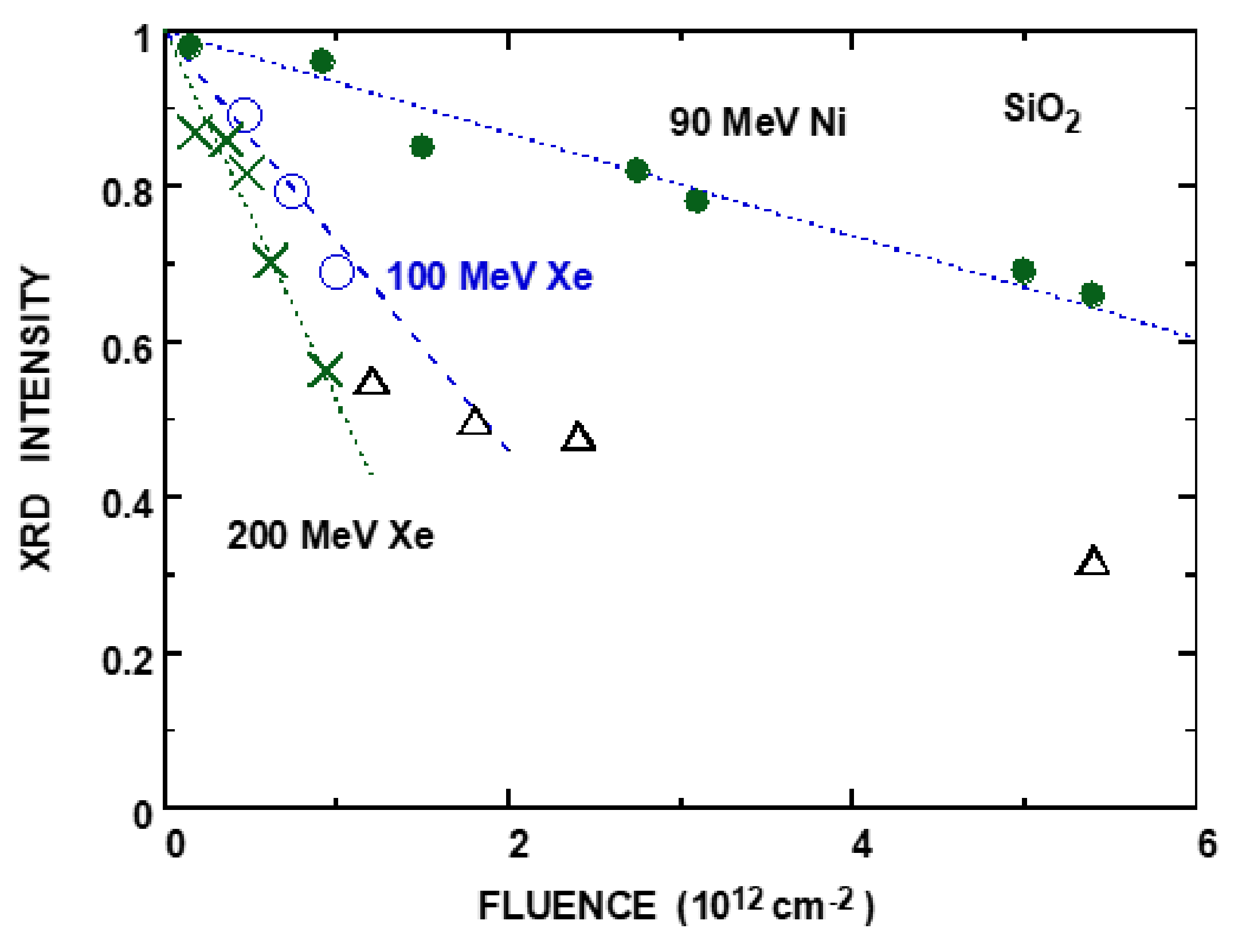
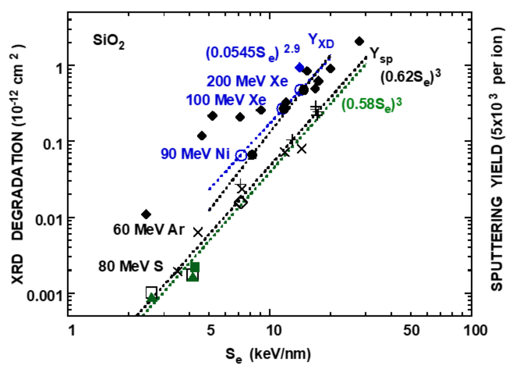
3.1. SiO2
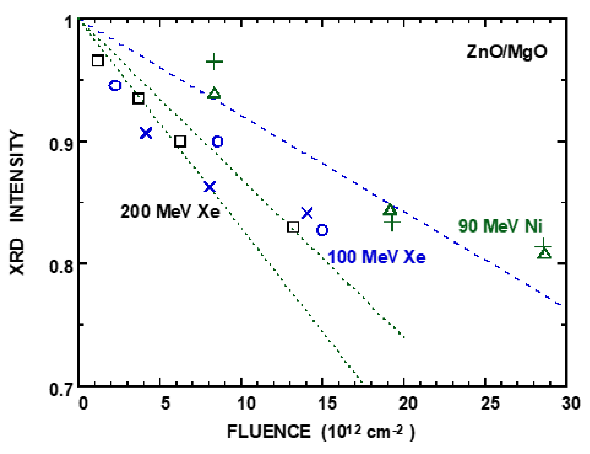
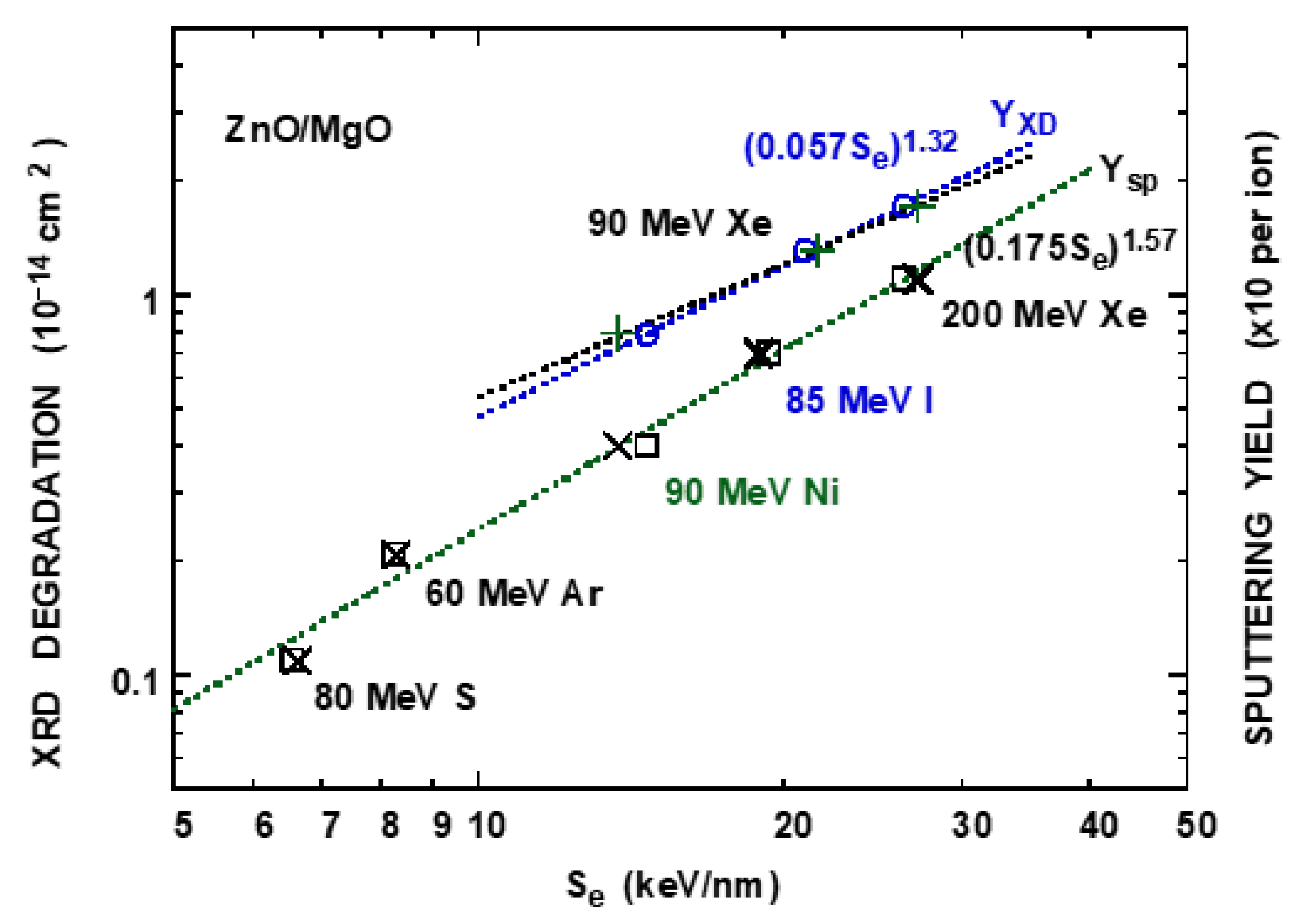
3.2. ZnO
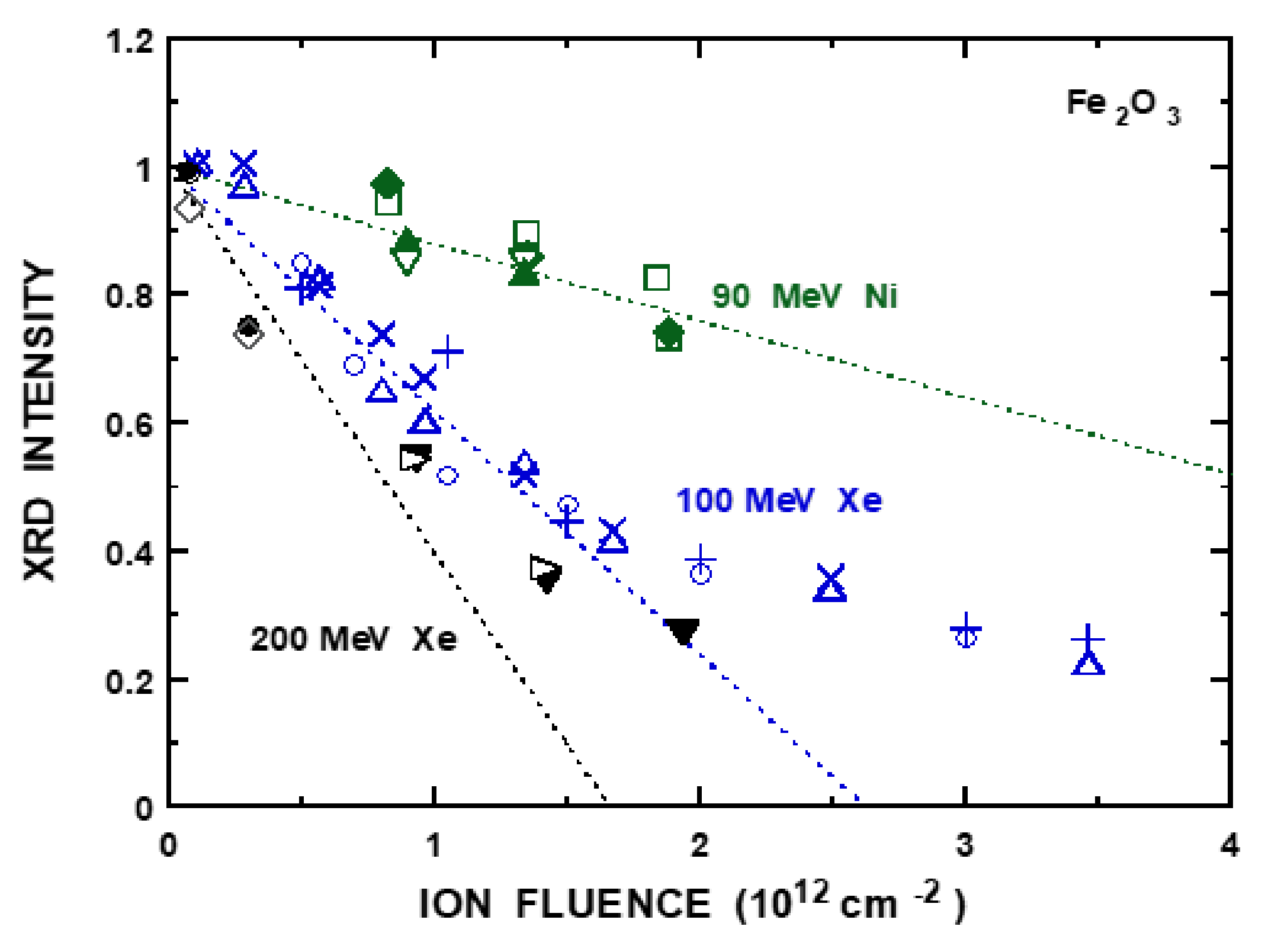
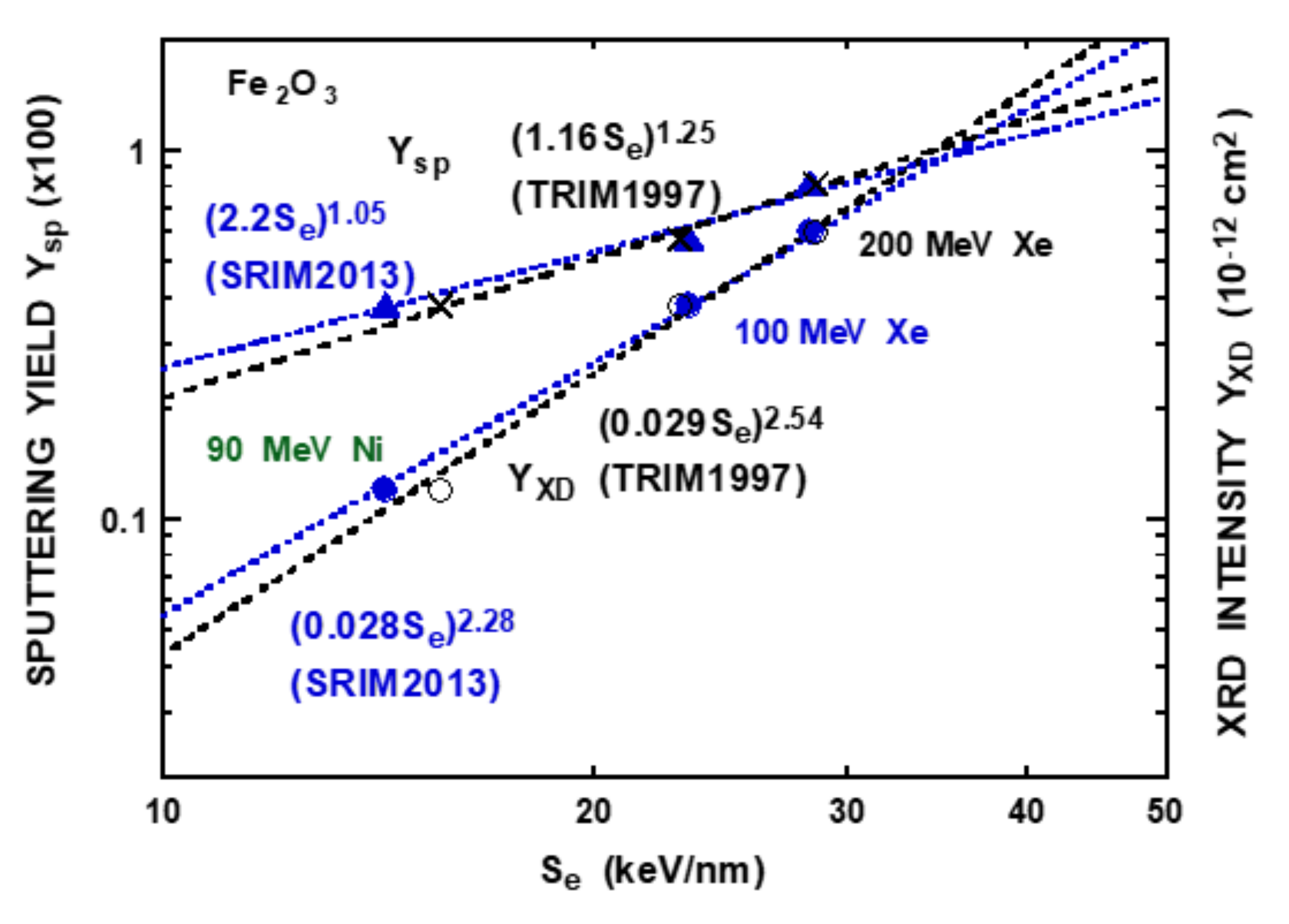
3.3. Fe2O3
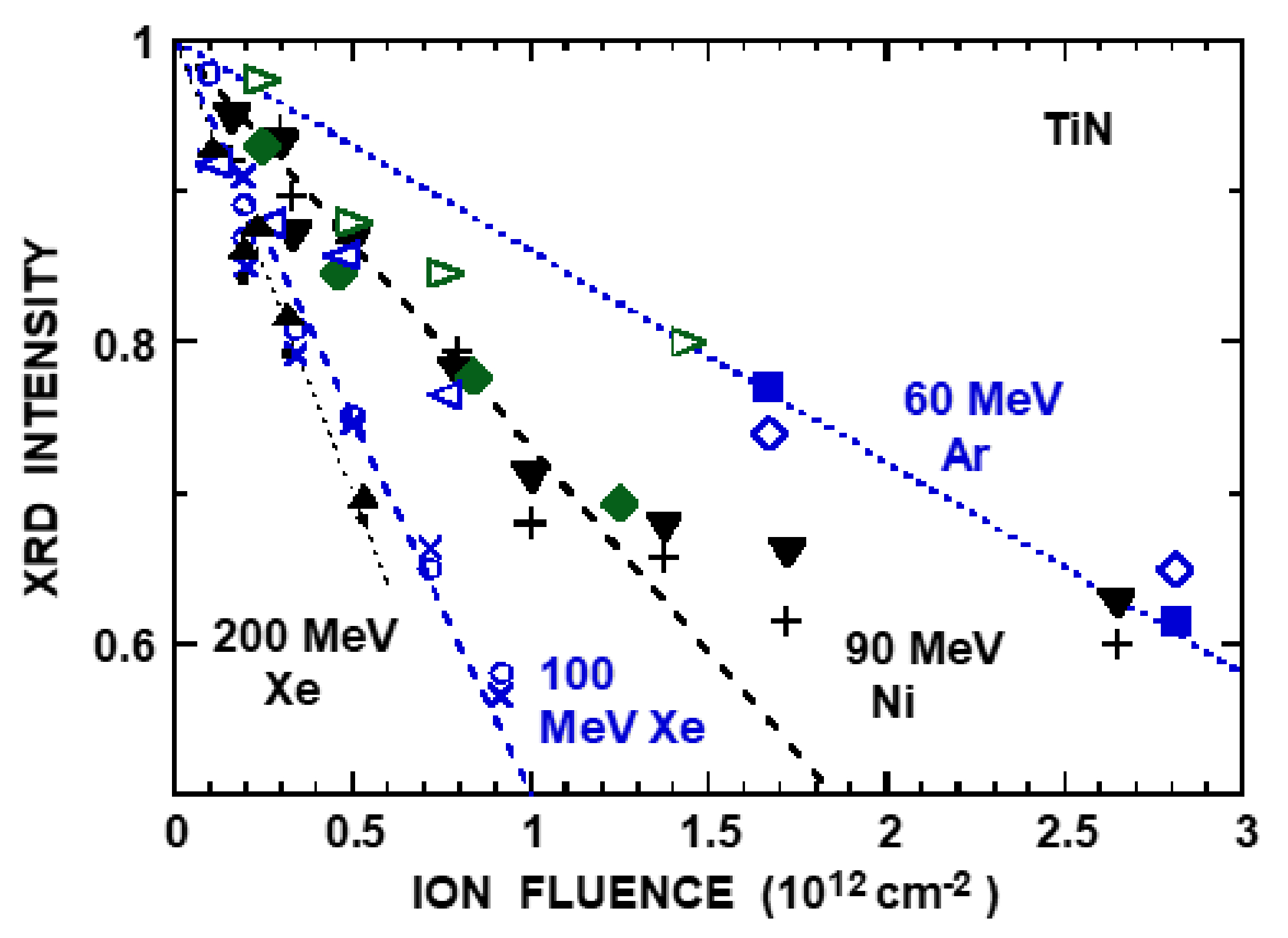
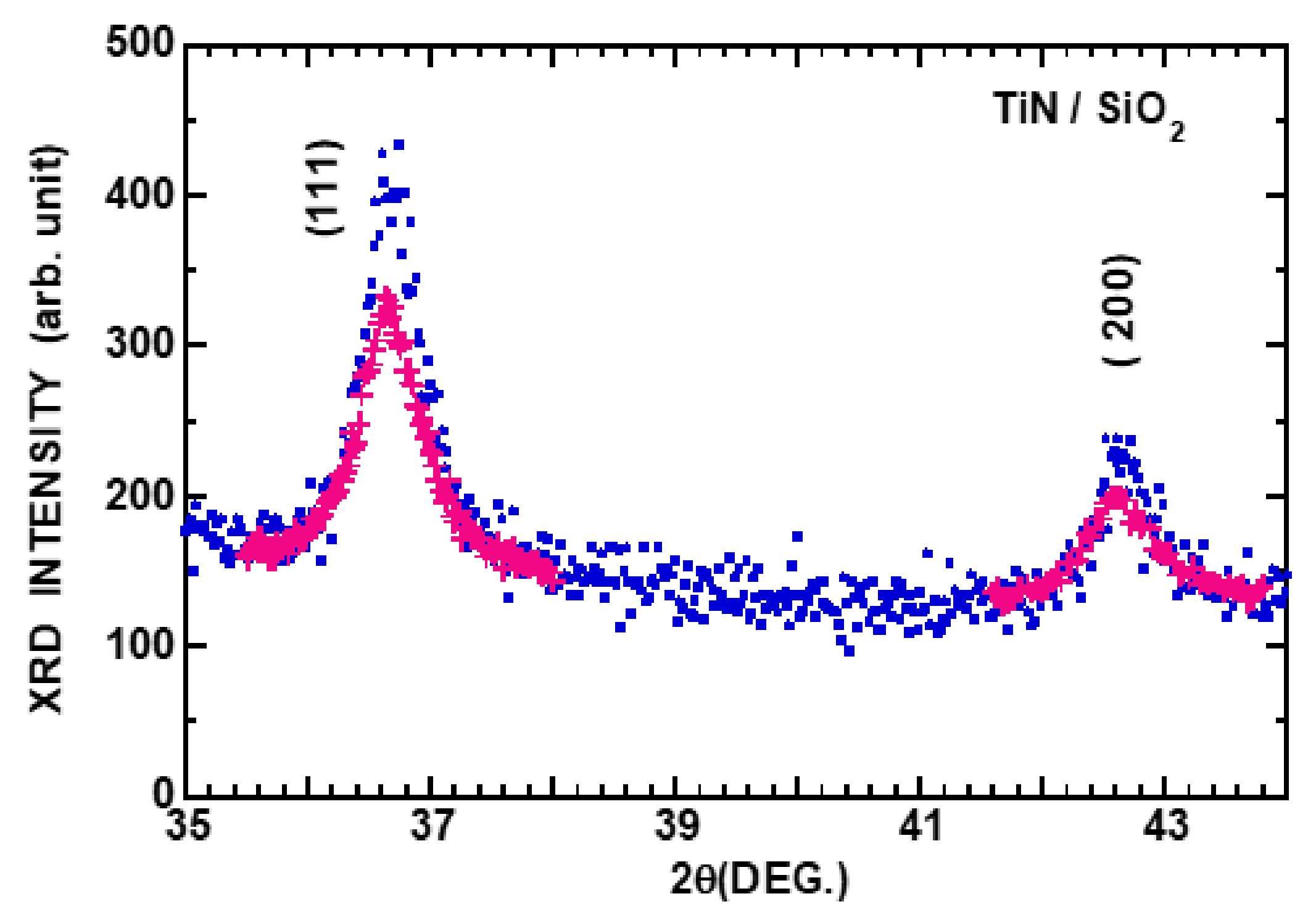
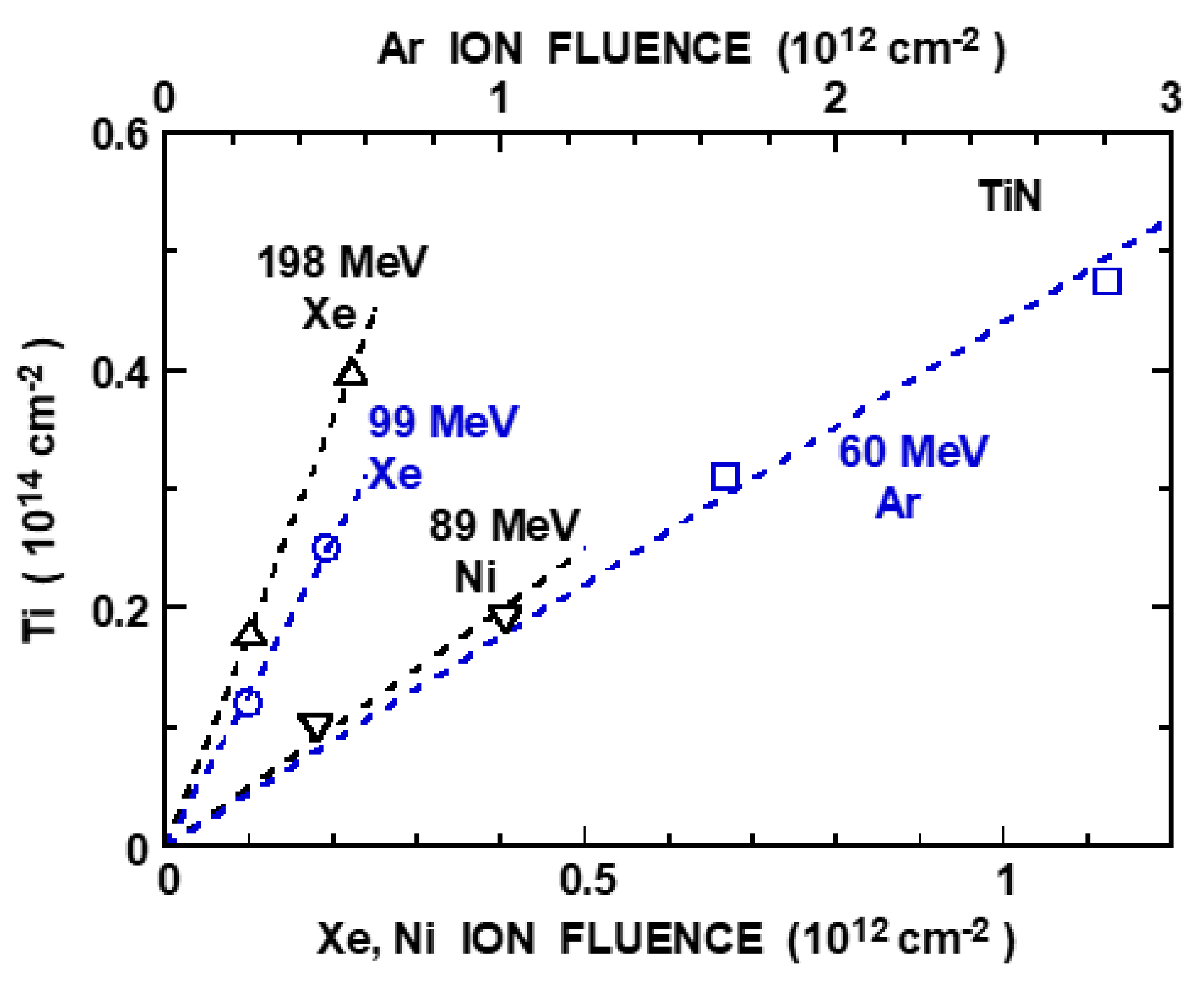
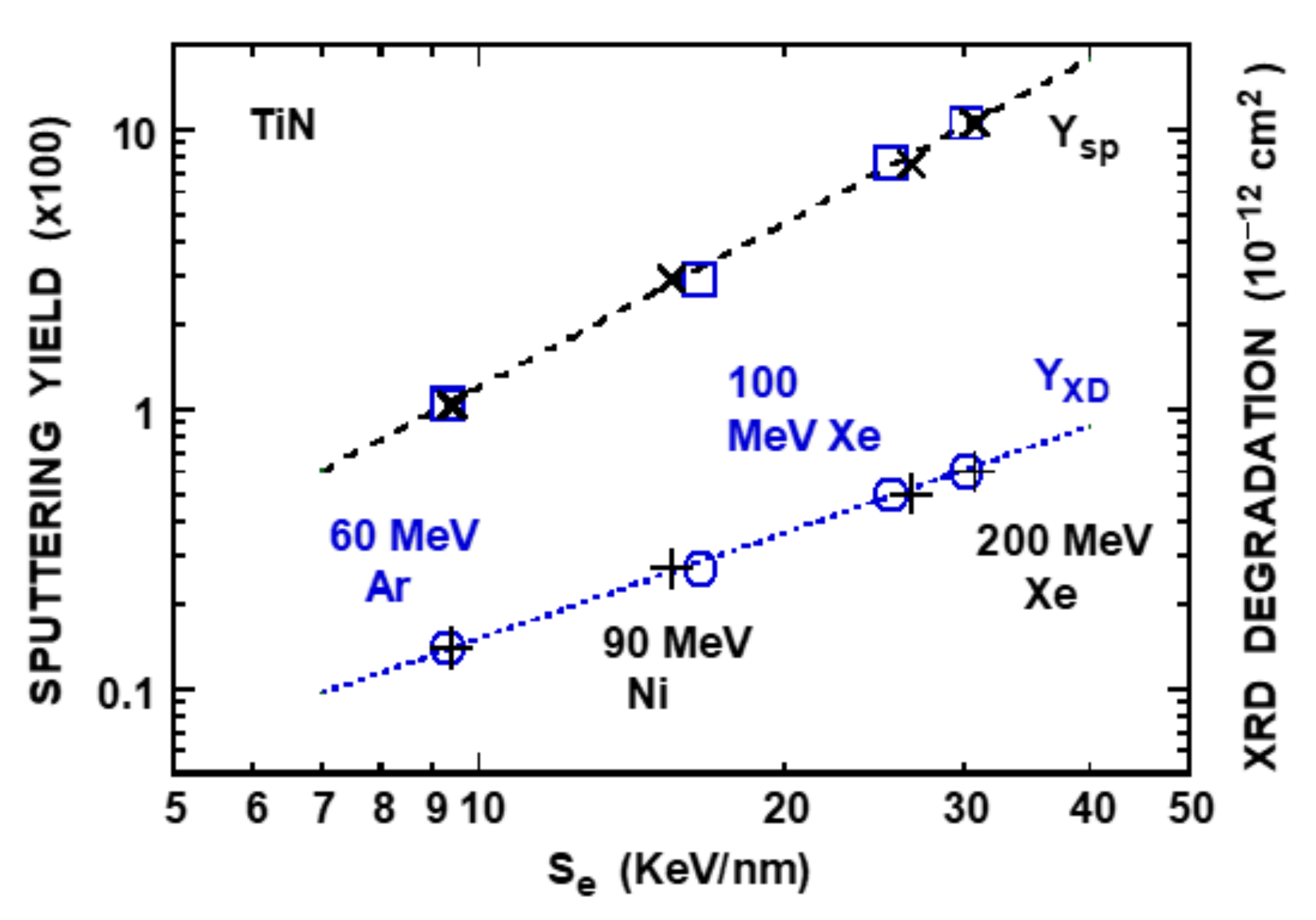
3.4. TiN
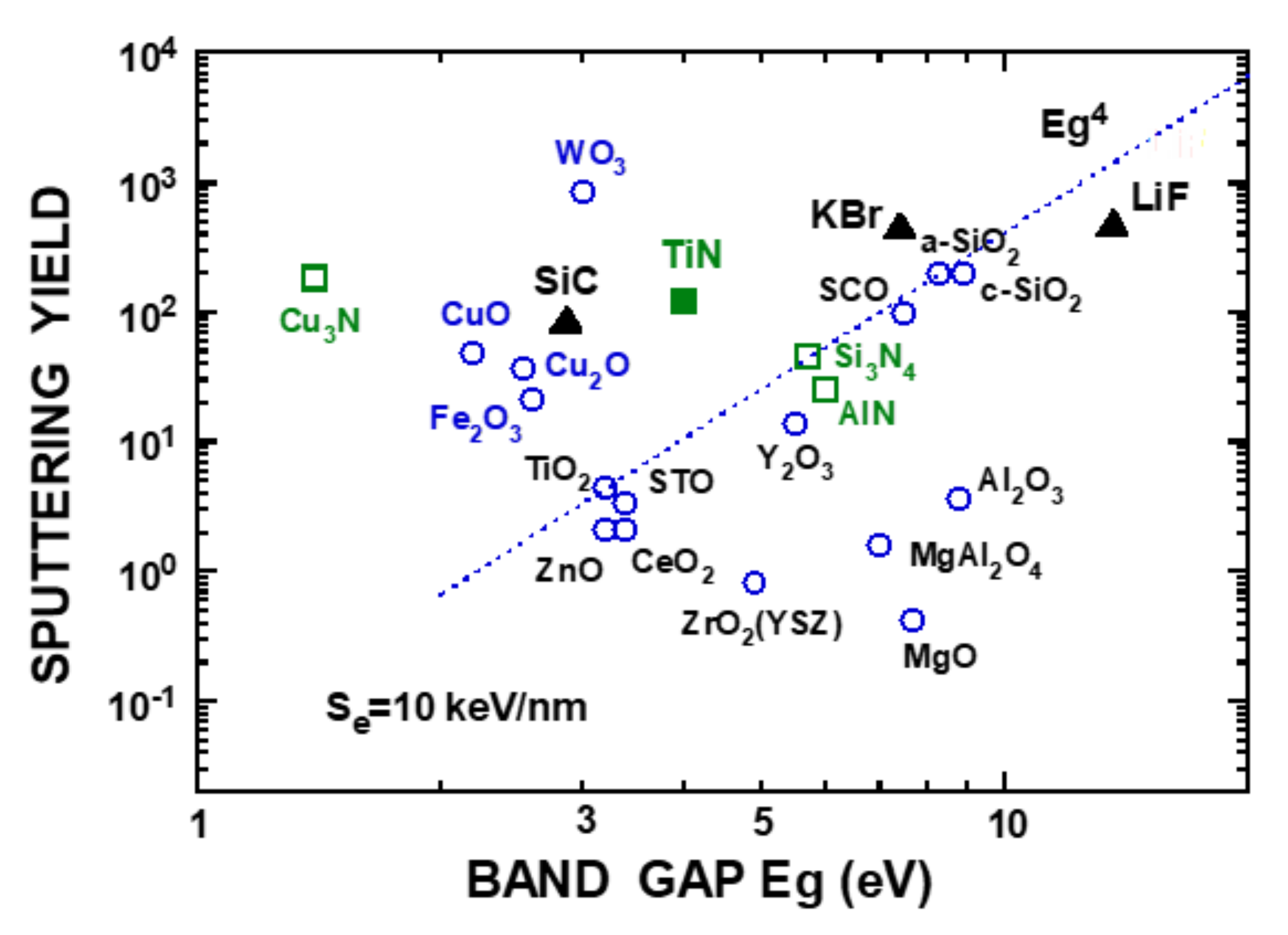
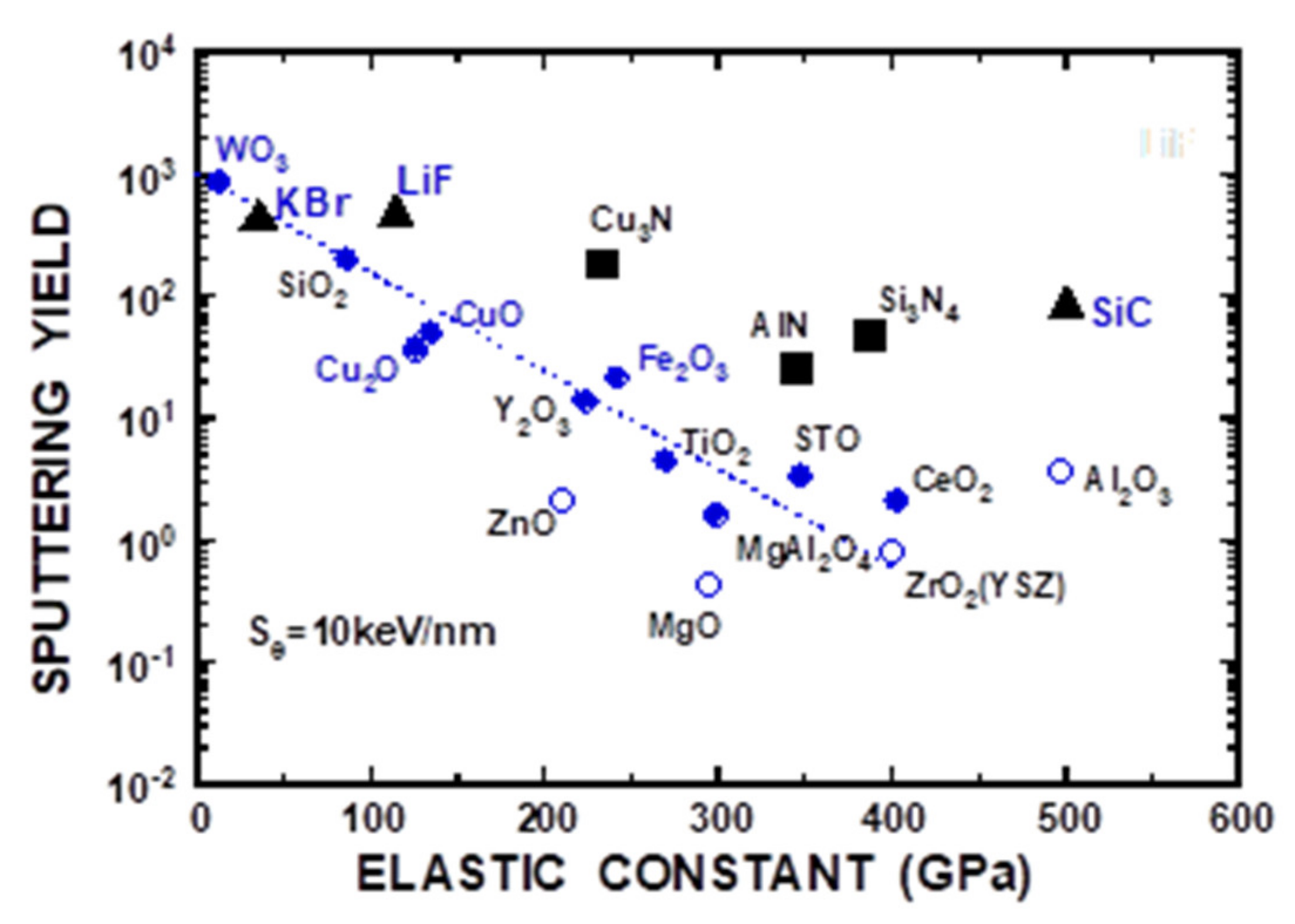
4. Discussion
4.1. Comparison of Lattice Disordering with Sputtering
4.2. Electron–Lattice Coupling
5. Conclusions
Author Contributions
Funding
Institutional Review Board Statement
Informed Consent Statement
Data Availability Statement
Acknowledgments
Conflicts of Interest
References
- Young, D.A. Etching of Radiation Damage in Lithium Fluoride. Nature 1958, 182, 375–377. [Google Scholar] [CrossRef] [PubMed]
- Silk, E.C.H.; Barnes, R.S. Examination of Fission Fragment Tracks with an Electron Microscope. Phil. Mag. 1959, 4, 970–972. [Google Scholar] [CrossRef]
- Fleischer, R.L.; Price, P.B.; Walker, R.M. Ion Explosion Spike Mechanism for Formation of Charged-Particle Tracks in Solids. J. Appl. Phys. 1965, 36, 3645–3652. [Google Scholar] [CrossRef]
- Fleischer, R.L. Tracks to Innovation; Springer: New York, NY, USA, 1998; pp. 1–193. [Google Scholar]
- Meftah, A.; Brisard, F.; Costantini, J.M.; Dooryhee, E.; Hage-Ali, M.; Hervieu, M.; Stoquert, J.P.; Studer, F.; Toulemonde, M. Track formation in SiO2 quartz and the thermal-spike mechanism. Phys. Rev. B 1994, 49, 12457–12463. [Google Scholar] [CrossRef]
- Toulemonde, M.; Bouffard, S.; Studer, F. Swift heavy ions in insulating and conducting oxides: Tracks and physical properties. Nucl. Instr. Meth. B 1994, 91, 108–123. [Google Scholar] [CrossRef]
- Ramos, S.M.M.; Bonardi, N.; Canut, B.; Bouffard, S.; Della-Negra, S. Damage creation in α-Al2O3 by MeV fullerene impacts. Nucl. Instr. Meth. B 1998, 143, 319–332. [Google Scholar] [CrossRef]
- Skuratov, V.A.; Zinkle, S.J.; Efimov, A.E.; Havancsak, K. Surface defects in Al2O3 and MgO irradiated with high-energy heavy ions. Surf. Coat. Technol. 2005, 196, 56–62. [Google Scholar] [CrossRef]
- Khalfaoui, N.; Stoquert, J.P.; Haas, F.; Trautmann, C.; Meftah, A.; Toulemonde, M. Damage creation threshold of Al2O3 under swift heavy ion irradiation. Nucl. Instr. Meth. B 2012, 286, 247–253. [Google Scholar] [CrossRef]
- O’Connell, J.H.; Rymzhanov, R.A.; Skuratov, V.A.; Volkov, A.E.; Kirilkin, N.S. Latent tracks and associated strain in Al2O3 irradiated with swift heavy ions. Nucl. Instr. Meth. B 2016, 374, 97–101. [Google Scholar] [CrossRef]
- Kluth, P.; Pakarinen, O.H.; Djurabekova, F.; Giulian, R.; Ridgway, M.C.; Byrne, A.P. Nanoscale density fluctuations in swift heavy ion irradiated amorphous SiO2. J. Appl. Phys. 2011, 110, 123520. [Google Scholar] [CrossRef] [Green Version]
- Benyagoub, A.; Toulemonde, M. Ion tracks in amorphous silica. J. Mater. Res. 2015, 30, 1529–1543. [Google Scholar] [CrossRef]
- Zinkle, S.J.; Skuratov, V.A.; Hoelzer, D.T. On the conflicting roles of ionizing radiation in ceramics. Nucl. Instr. Meth. B 2002, 191, 758–766. [Google Scholar] [CrossRef]
- Van Vuuren, A.J.; Ibrayeva, A.D.; Skuratov, V.A.; Zdorovets, M.V. Analysis of the microstructural evolution of silicon nitride irradiated with swift Xe ions. Ceram. Int. 2020, 46, 7155–7160. [Google Scholar] [CrossRef]
- Kitayama, T.; Morita, Y.; Nakajima, K.; Narumi, K.; Saitoh, Y.; Matsuda, M.; Sataka, M.; Tsujimoto, M.; Isoda, S.; Toulemonde, M.; et al. Formation of ion tracks in amorphous silicon nitride films with MeV C60 ions. Nucl. Instr. Meth. B 2015, 356–357, 22–27. [Google Scholar] [CrossRef]
- Mota-Santiago, P.; Vazquez, H.; Bierschenk, T.; Kremer, F.; Nadzri, A.; Schauries, D.; Djurabekova, F.; Nordlund, K.; Trautmann, C.; Mudie, S.; et al. Nanoscale density variations induced by high energy heavy ions in amorphous silicon nitride and silicon dioxide. Nanotechnology 2018, 29, 144004. [Google Scholar] [CrossRef] [Green Version]
- Kucheyev, S.O.; Timmers, H.; Zou, J.; Williams, J.S.; Jagadish, C.; Li, G. Lattice damage produced in GaN by swift heavy ions. J. Appl. Phys. 2004, 95, 5360–5365. [Google Scholar] [CrossRef] [Green Version]
- Mansouri, S.; Marie, P.; Dufour, C.; Nouet, G.; Monnet, I.; Lebius, H.; Benamara, Z.; Al-Douri, Y. Swift heavy ion effects in gallium nitride. Int. J. Nanoelectron. Mater. 2008, 1, 101–106. [Google Scholar]
- Sall, M.; Monnet, I.; Moisy, F.; Grygiel, C.; Grygiel, C.; Jubolt-Leclerc, S.; Della-Negra, S.; Toulemonde, M.; Balanzat, E. Track formation in III-N semiconductors irradiated by swift heavy ions and fullerene and re-evaluation of the inelastic thermal spike model. J. Mater Sci. 2015, 50, 5214–5227. [Google Scholar] [CrossRef]
- Moisy, F.; Sall, M.; Grygiel, C.; Ribet, A.; Balanzat, E.; Monnet, I. Optical bandgap and stress variations induced by the formation of latent tracks in GaN under swift heavy ion irradiation. Nucl. Instr. Meth. B 2018, 431, 12–18. [Google Scholar] [CrossRef]
- Kamarou, A.; Wesch, W.; Wendler, E.; Undisz, A.; Rettenmayr, M. Swift heavy ion irradiation of InP: Thermal spike modeling of track formation. Phys. Rev. B 2006, 73, 184107. [Google Scholar] [CrossRef]
- Ochedowski, O.; Osmani, O.; Schade, M.; Bussmann, B.K.; Ban-d’Etat, B.; Lebius, H.; Schleberger, M. Graphitic nanostripes in silicon carbide surfaces created by swift heavy ion irradiation. Nat. Commun. 2014, 5, 3913. [Google Scholar] [CrossRef] [PubMed]
- Alencar, I.; Silva, M.R.; Leal, R.; Grande, P.L.; Papaleo, R.M. Impact Features Induced by Single Fast Ions of Different Charge-State on Muscovite Mica. Atoms 2021, 9, 17. [Google Scholar] [CrossRef]
- Okubo, N.; Ishikawa, N.; Sataka, M.; Jitsukawa, S. Surface amorphization in Al2O3 induced by swift heavy ion irradiation. Nucl. Instr. Meth. B 2013, 314, 208–210. [Google Scholar] [CrossRef]
- Grygiel, C.; Moisy, F.; Sall, M.; Lebius, H.; Balanzat, E.; Madi, T.; Been, T.; Marie, D.; Monnet, I. In-situ kinetics of modifications induced by swift heavy ions in Al2O3: Colour center formation, structural modification and amorphization. Acta Mater. 2017, 140, 157–167. [Google Scholar] [CrossRef]
- Dhar, S.; Bolse, W.; Lieb, K.-P. Ion-beam induced amorphization and dynamic epitaxial recrystallization in α-quartz. J. Appl. Phys. 1999, 85, 3120–3123. [Google Scholar] [CrossRef]
- Rymzhanov, R.A.; Medvedev, N.; O’Connell, J.H.; van Vuuren, A.J.; Skuratov, V.A.; Evolkov, A.E. Recrystallization as the governing mechanism of ion track formation. Sci. Rep. 2019, 9, 3837. [Google Scholar] [CrossRef]
- Williams, J.S. Damage Formation, Amorphization and Crystallization in Semiconductors at Elevated Temperature. Chapter 6. In Ion Beam Modification of Solids; Wesch, W., Wendler, E., Eds.; Springer: Berlin, Germany, 2016; pp. 243–285. [Google Scholar]
- Gupta, S.; Gehrke, H.G.; Krauser, J.; Trautmann, C.; Severin, D.; Bender, M.; Rothard, H.; Hofsass, H. Conducting ion tracks generated by charge-selected swift heavy ions. Nucl. Instr. B 2016, 381, 76–83. [Google Scholar] [CrossRef]
- Itoh, N.; Duffy, D.M.; Khakshouri, S.; Stoneham, A.M. Making tracks: Electronic excitation roles in forming swift heavy ion tracks. J. Phys. Condens. Matter 2009, 21, 474205. [Google Scholar] [CrossRef] [Green Version]
- Rogers, M.D. Mass Transport and Grain Growth induced by Fission Fragments in Thin Films of Uranium Dioxide. J. Nucl. Mater. 1965, 16, 298–305. [Google Scholar] [CrossRef]
- Rogers, M.D. Ejection of Uranium Atoms from Sintered UO2. J. Nucl. Mater. 1967, 22, 103–105. [Google Scholar] [CrossRef]
- Nilsson, G. Ejection of Uranium Atoms from Sintered UO2 by Fission Fragments in Different Gases and at Different Gas Pressures. J. Nucl. Mater. 1966, 20, 215–230. [Google Scholar] [CrossRef]
- Meins, C.K.; Griffith, J.E.; Qiu, Y.; Mendenhall, M.H.; Seiberling, L.E.; Tombrello, T.A. Sputtering of UF4 by High Energy Heavy Ions. Rad. Eff. 1983, 71, 13–33. [Google Scholar] [CrossRef]
- Bouffard, S.; Duraud, J.P.; Mosbah, M.; Schlutig, S. Angular distribution of the sputtered atoms from UO2 under high electronic stopping power irradiation. Nucl. Instr. Meth. B 1998, 141, 372–377. [Google Scholar] [CrossRef]
- Schlutig, S. Contribution a L’etude de la Pulverisation et de L’endommagement du Dioxyde D’uranuim par les Ions Lourds Rapides. Ph.D. Thesis, University of Caen, Caen, France, March 2001. [Google Scholar]
- Brown, W.L.; Lanzerotti, L.J.; Poate, J.M.; Augustyniak, W.M. “Sputtering” of Ice by MeV Light Ions. Phys. Rev. Lett. 1978, 40, 1027–1030. [Google Scholar] [CrossRef]
- Brown, W.L.; Augustyniak, W.M.; Brody, E.; Cooper, B.; Lanzerotti, L.J.; Ramirez, A.; Evatt, R.; Johnson, R.E. Energy Dependence of the Erosion of H2O Ice Films by H and He Ions. Nucl. Instr. Meth. 1980, 170, 321–325. [Google Scholar] [CrossRef]
- Bottiger, J.; Davies, J.A.; L’Ecuyer, J.; Matsunami, N.; Ollerhead, R. Erosion of Frozen-Gas Films by MeV Ions. Rad. Eff. 1980, 49, 119–124. [Google Scholar] [CrossRef]
- Baragiora, R.A.; Vidal, R.A.; Svendsen, W.; Schou, J.; Shi, M.; Bahr, D.A.; Atteberrry, C.L. Sputtering of water ice. Nucl. Instr. Meth. B 2003, 209, 294–303. [Google Scholar] [CrossRef]
- Dartois, E.; Auge, B.; Boduch, P.; Brunetto, R.; Chabot, M.; Domaracka, A.; Ding, J.J.; Kamalou, O.; Lv, X.Y.; Rothard, H.; et al. Heavy ion irradiation of crystalline ice: Cosmic ray amorphisation cross-section and sputtering yield. Astron. Astrophys. 2015, 576, A125. [Google Scholar] [CrossRef] [Green Version]
- Galli, A.; Vorburger, A.; Wurz, P.; Tulej, M. Sputtering of water ice films: A re-assessment with singly and doubly charged oxygen and argon ions, molecular oxygen, and electrons. Icarus 2017, 291, 36–45. [Google Scholar] [CrossRef] [Green Version]
- Brown, W.L.; Lanzerotti, L.J.; Marcantonio, K.J.; Johnson, R.E.; Reimann, C.T. Sputtering of Ices by High Energy Particle Impact. Nucl. Instr. Meth. B 1986, 14, 392–402. [Google Scholar] [CrossRef]
- Mejia, C.; Bender, M.; Severin, D.; Trautmann, C.; Boduch, P.H.; Bordalo, V.; Domaracka, A.; Lv, X.Y.; Martinez, R.; Rothard, H. Radiolysis and sputtering of carbon dioxide ice induced by swift Ti, Ni and Xe ions. Nucl. Instr. Meth. B 2015, 365, 477–481. [Google Scholar] [CrossRef]
- Qiu, Y.; Griffith, J.E.; Meng, W.J.; Tombrello, T.A. Sputtering of Silicon and its Compounds in the Electronic Stopping Region. Rad. Eff. 1983, 70, 231–236. [Google Scholar] [CrossRef]
- Sugden, S.; Sofield, C.J.; Murrell, M.P. Sputtering by MeV ions. Nucl. Instr. Meth. B 1992, 67, 569–573. [Google Scholar] [CrossRef]
- Matsunami, N.; Sataka, M.; Iwase, A. Electronic sputtering of oxides by high energy ion impact. Nucl. Instr. Meth. B 2002, 193, 830–834. [Google Scholar] [CrossRef]
- Matsunami, N.; Fukuoka, O.; Shimura, T.; Sataka, M.; Okayasu, S. A multi-exciton model for the electronic sputtering of oxides. Nucl. Instr. Meth. B 2005, 230, 507–511. [Google Scholar] [CrossRef]
- Arnoldbik, W.M.; Tomozeiu, N.; Habraken, F.H.P.M. Electronic sputtering of thin SiO2 films by MeV heavy ions. Nucl. Instr. Meth. B 2003, 203, 151–157. [Google Scholar] [CrossRef]
- Toulemonde, M.; Assmann, W.; Trautmann, C.; Gruner, F. Jetlike Component in Sputtering of LiF Induced by Swift Heavy Ions. Phys. Rev. Lett. 2002, 88, 057602. [Google Scholar] [CrossRef]
- Toulemonde, M.; Assmann, W.; Trautmann, C. Electronic sputtering of vitreous SiO2: Experimental and modeling results. Nucl. Instr. Meth B 2016, 379, 2–8. [Google Scholar] [CrossRef]
- Griffith, J.E.; Weller, R.A.; Seiberling, L.E.; Tombrello, T.A. Sputtering of Uranium Tetrafluoride in the Electronic Stopping Region. Rad. Eff. 1980, 51, 223–232. [Google Scholar] [CrossRef]
- Toulemonde, M.; Assmann, W.; Muller, D.; Trautmann, C. Electronic sputtering of LiF, CaF2, LaF3 and UF4 with 197 MeV Au ions: Is the stoichiometry of atom emission preserved? Nucl. Instr. Meth. B 2017, 406, 501–507. [Google Scholar] [CrossRef]
- Matsunami, N.; Sataka, M.; Iwase, A.; Okayasu, S. Electronic excitation induced sputtering of insulating and semiconducting oxides by high energy heavy ions. Nucl. Instr. Meth. B 2003, 209, 288–293. [Google Scholar] [CrossRef]
- Matsunami, N.; Sataka, M.; Okayasu, S.; Tazawa, M. Electronic sputtering of nitrides by high-energy ions. Nucl. Instr. B 2007, 256, 333–336. [Google Scholar] [CrossRef]
- Matsunami, N.; Okayasu, S.; Sataka, M.; Tsuchiya, B. Electronic sputtering of SiC and KBr by high energy ions. Nucl. Instr. Meth. B 2020, 478, 80–84. [Google Scholar] [CrossRef]
- Matsunami, N.; Sataka, M.; Okayasu, S.; Ishikawa, N.; Tazawa, M.; Kakiuchida, H. High-energy ion irradiation effects on atomic structures and optical properties of copper oxide and electronic sputtering. Nucl. Instr. Meth. B 2008, 266, 2986–2989. [Google Scholar] [CrossRef]
- Matsunami, N.; Sataka, M.; Okayasu, S.; Kakiuchida, H. Ion irradiation effects on tungsten-oxide films and charge state effect on electronic erosion. Nucl. Instr. Meth. B 2010, 268, 3167–3170. [Google Scholar] [CrossRef]
- Matsunami, N.; Sakuma, Y.; Sataka, M.; Okayasu, S.; Kakiuchida, H. Electronic sputtering of CuO films by high-energy ions. Nucl. Instr. Meth. B 2013, 314, 55–58. [Google Scholar] [CrossRef]
- Matsunami, N.; Okayasu, S.; Sataka, M. Electronic excitation effects on Fe2O3 films by high-energy ions. Nucl. Instr. Meth. B 2018, 435, 142–145. [Google Scholar] [CrossRef]
- Matsunami, N.; Kakiuchida, H.; Tazawa, M.; Sataka, M.; Sugai, H.; Okayasu, S. Electronic and atomic structure modifications of copper nitride films by ion impact and phase separation. Nucl. Instr. Meth. B 2009, 267, 2653–2656. [Google Scholar] [CrossRef]
- Assmann, W.; d’Etat, B.B.; Bender, M.; Boduch, P.; Grande, P.L.; Lebius, H.; Lelievre, D.; Marmitt, G.G.; Rothard, H.; Seidl, T.; et al. Charge-state related effects in sputtering of LiF by swift heavy ions. Nucl. Instr. Meth B 2017, 392, 94–101. [Google Scholar] [CrossRef]
- Toulemonde, M.; Assmann, W.; Ban-d’Etat, B.; Bender, M.; Bergmaier, A.; Boduch, P.; Della-Negra, S.; Duan, J.; El-Said, A.S.; Gruner, F.; et al. Sputtering of LiF and other halide crystals in the electronic energy loss regime. Eur. Phys. J. D 2020, 74, 144. [Google Scholar] [CrossRef]
- Matsunami, N.; Sataka, M.; Okayasu, S.; Tsuchiya, B. Charge State Effect of High Energy Ions on Material Modification in the Electronic Stopping Region. Atoms 2021, 9, 36. [Google Scholar] [CrossRef]
- Ziegler, J.F.; Biersack, J.P.; Littmark, U. The Stopping and Range of Ions in Solids; Pergamon Press: New York, NY, USA, 1985; pp. 1–321. [Google Scholar]
- Ziegler, J.F.; Ziegler, M.D.; Biersack, J.P. SRIM-The stopping and range of ions in matter (2010). Nucl. Instr. Meth. B 2010, 268, 1818–1823. [Google Scholar] [CrossRef] [Green Version]
- Grande, P.L.; Schiwietz, G. Convolution approximation for the energy loss, ionization probability and straggling of fast ions. Nucl. Instr. Meth. B 2009, 267, 859–865. [Google Scholar] [CrossRef] [Green Version]
- Matsunami, N.; Sataka, M.; Iwase, A. Sputtering of high Tc superconductor YBa2Cu3O7-δ by high energy heavy ions. Nucl. Instr. Meth. B 2001, 175-177, 56–61. [Google Scholar] [CrossRef]
- Meftah, A.; Assmann, W.; Khalfaoui, N.; Stoquert, J.P.; Studer, F.; Toulemonde, M.; Trautmann, C.; Voss, K.-O. Electronic sputtering of Gd3Ga5O12 and Y3Fe5O12 garnets: Yield, stoichiometry and comparison to track formation. Nucl. Instr. Meth. B 2011, 269, 955–958. [Google Scholar] [CrossRef]
- Shinde, N.S.; Matsuanmi, N.; Shimura, T.; Sataka, M.; Okayasu, S.; Kato, T.; Tazawa, M. Alignment of grain orientation in polycrystalline-SiO2 films induced by high-energy heavy ions. Nucl. Instr. Meth. B 2006, 245, 231–234. [Google Scholar] [CrossRef]
- Matsunami, N.; Itoh, M.; Kato, M.; Okayasu, S.; Sataka, M.; Kakiuchida, H. Ion induced modifications of Mn-doped ZnO films. Nucl. Instr. Meht. B 2015, 365, 191–195. [Google Scholar] [CrossRef]
- Matsunami, N.; Kato, M.; Sataka, M.; Okayasu, S. Disordering of ultra thin WO3 films by high-energy ions. Nucl. Instr. Meth. B 2017, 409, 272–276. [Google Scholar] [CrossRef]
- Matsunami, N.; Sogawa, T.; Sakuma, Y.; Ohno, N.; Tokitani, M.; Masuzaki, S. Deuterium retention in Fe2O3 under low-energy deuterium-plasma exposure. Phys. Scr. T 2011, 145, 014042. [Google Scholar] [CrossRef]
- Matsunami, N.; Ohno, N.; Tokitani, M.; Tsuchiya, B.; Sataka, M.; Okayasu, S. Modifications of WNOx films by keV D and H ions. Surf. Coat. Technol. 2020, 394, 125798. [Google Scholar] [CrossRef]
- Matsunami, N.; Okayasu, S.; Sataka, M.; Tsuchiya, B. Ion irradiation effects on WNxOy thin films. Nucl. Instr. Meth. B 2018, 435, 146–151. [Google Scholar] [CrossRef]
- Matsunami, N.; Teramoto, T.; Okayasu, S.; Sataka, M.; Tsuchiya, B. Modifications of WNxOy films by ion impact. Surf. Coat. Technol. 2018, 355, 84–89. [Google Scholar] [CrossRef]
- Matsunami, N.; Itoh, M.; Takai, Y.; Tazawa, M.; Sataka, M. Ion beam modification of ZnO thin films on MgO. Nucl. Instr. Meth. B 2003, 206, 282–286. [Google Scholar] [CrossRef]
- Matsunami, N.; Itoh, M.; Kato, M.; Okayasu, S.; Sataka, M.; Kakiuchida, H. Growth of Mn-doped ZnO thin films by rf-sputter deposition and lattice relaxation by energetic ion impact. Appl. Surf. Sci. 2015, 350, 31–37. [Google Scholar] [CrossRef]
- Joint Committee on Powder Diffraction Standards (JCPDS). JCPDS File 381420; International Centre for Diffraction Data (ICDD): Newtown Square, PA, USA.
- Storm, E.; Israel, H.I. Photon Cross Sections from 1 keV to 100 MeV for Elements Z = 1 to Z = 100. Atom. Data Nucl. Data Tables 1970, 7, 565–681. [Google Scholar] [CrossRef]
- Shima, K.; Kuno, N.; Yamanouchi, M.; Tawara, H. Equilibrium Charge Fractions of Ions of Z = 4–92 Emerging from a Carbon Foil. Atom. Data Nucl. Data Tables 1992, 51, 173–241. [Google Scholar] [CrossRef]
- Schiwietz, G.; Grande, P.L. Improved charge-state formulas. Nucl. Instr. Meth B 2001, 175–177, 125–131. [Google Scholar] [CrossRef]
- DuBois, R.D.; Santos, A.C.F.; Olson, R.E. Scaling laws for electron loss from ion beams. Nucl. Instr. Meth. A 2005, 544, 497–501. [Google Scholar] [CrossRef]
- DuBois, R.D.; Santos, A.C.F. Target-Scaling Properties for Electron Loss by Fast Heavy Ions (Chapter 8). In Atomic Processes in Basic and Applied Physics; Shevelko, V., Tawara, H., Eds.; Springer: Berlin, Germany, 2012; pp. 185–209. [Google Scholar]
- Lide, D.R. (Ed.) CRC Handbook of Chemistry and Physics, 84th ed.; CRC Press: Boca Raton, FL, USA, 2003. [Google Scholar]
- Rodrigues, G.C.; Indelicato, P.; Santos, J.P.; Patte, P.; Parente, F. Systematic calculation of total atomic energies of ground state configurations. Atom. Data Nucl. Data Tables 2004, 86, 117–233. [Google Scholar] [CrossRef]
- Sigmund, P. Sputtering by Ion Bombardment: Theoretical Concepts. Chapter 2. In Sputtering by Particle Bombardment; Behrisch, R., Ed.; Springer: Berlin, Germany, 1981; Volume 1, pp. 9–71. [Google Scholar]
- Betz, G.; Wehner, G.K. Sputtering of Multicomponent Materials. Chapter 2. In Sputtering by Particle Bombardment; Behrisch, R., Ed.; Springer: Berlin, Germany, 1983; Volume 2, pp. 11–90. [Google Scholar]
- Paul, H. The Stopping Power of Matter for Positive Ions. Chapter 7. In Modern Practices in Radiation Therapy; Natanasabapathi, G., Ed.; InTech: Rijeka, Croatia, 2012; pp. 113–132. [Google Scholar]
- Besenbacher, F.; Bottiger, J.; Graversen, O.; Hansen, J.L.; Sorensen, H. Stopping power of solid argon for helium ions. Nucl. Instr. Meth. 1981, 188, 657–667. [Google Scholar] [CrossRef]
- Kittel, C. Introduction to Solid State Physics, 6th ed.; John Wiley & Sons Inc.: New York, NY, USA, 1986; pp. 1–646. [Google Scholar]
- ICRU Report 49. Stopping Powers and Ranges for Protons and Alpha Particles; International Commission on Radiation Units and Measurements: Bethesda, MD, USA, 1993; pp. 1–286. [Google Scholar]
- Arnau, A.; Bauer, P.; Kastner, F.; Salin, A.; Ponce, V.H.; Fainstein, P.D.; Echenique, P.M. Phase effect in the energy loss of hydrogen projectiles in zinc targets. Phys. Rev. B 1994, 49, 6470. [Google Scholar] [CrossRef]
- Ranjan, R.; Allain, J.P.; Hendricks, M.R.; Ruzic, D.N. Absolute sputtering yield of Ti/TiN by Ar+/N+ at 400–700 eV. J. Vac. Sci. Tech. A 2001, 19, 1004–1007. [Google Scholar] [CrossRef]
- Itoh, N. Creation of lattice defects by electronic excitation in alkali halides. Adv. Phys. 1982, 31, 491–551. [Google Scholar] [CrossRef]
- Itoh, N.; Stoneham, A.M. Materials Modification by Electronic Excitation; Cambridge University Press: Cambridge, UK, 2001; pp. 1–520. [Google Scholar]
- Duffy, D.M.; Daraszewicz, S.L.; Mulroue, J. Modeling the effects of electronic excitations in ionic-covalent materials. Nucl. Instr. Meth. B 2012, 277, 21–27. [Google Scholar] [CrossRef] [Green Version]
- Matsunami, N.; Sataka, M.; Okayasu, S. Effective depth of electronic sputtering of WO3 films by high-energy ions. Nucl. Instr. Meth. B 2019, 460, 185–188. [Google Scholar] [CrossRef]
- Popovic, M.; Novakovic, M.; Mitric, M.; Zhang, K.; Rakocevic, Z.; Bibic, N. Xenon implantation effects on the structural and optical properties of reactively sputtered titanium nitride thin films. Mat. Res. Bull. 2017, 91, 36–41. [Google Scholar] [CrossRef]
- Solovan, M.; Brus, V.V.; Maistruk, E.V.; Maryanchuk, P.D. Electrical and Optical Properties of TiN Films. Inorgan. Mat. 2014, 50, 40–45. [Google Scholar] [CrossRef]
- Kavitha, A.; Kannan, R.; Reddy, P.S.; Rajashabala, S. The effect of annealing on the structural, optical and electrical properties of Titanium Nitride (TiN) thin films prepared by DC magnetron sputtering with supported discharge. J. Mat. Sci. Mat. Electron. 2016, 27, 10427–10434. [Google Scholar] [CrossRef]
- Martin, P.; Guizard, S.; Daguzan, P.; Petite, G.; D’Oliveira, P.; Meynadier, P.; Perdrix, M. Subpicosecond study of carrier trapping dynamics in wide-band-gap crystals. Phys. Rev. B 1997, 9, 5799–5810. [Google Scholar] [CrossRef]
- Nakajima, A.; Yoshihara, A.; Ishigame, M. Defect-induced Raman spectra in doped CeO2. Phys. Rev. B 1994, 50, 13297–13307. [Google Scholar] [CrossRef]
- Palko, J.W.; Kriven, W.M.; Sinogeikin, S.V.; Bass, J.D.; Sayir, A. Elastic constnts of yttria (Y2O3) monocrystals to high temperatures. J. Appl. Phys. 2001, 89, 7791–7796. [Google Scholar] [CrossRef]
- Kandil, H.M.; Greiner, J.D.; Smith, J.F. Single-Crystal Elastic Constnats of Yttria-Stabilized Ziroconia in the Range 20° to 700 °C. J. Am. Ceram. Soc. 1984, 67, 341–346. [Google Scholar] [CrossRef]
- Arab, M.; Dirany, N.; David, M. BAW resonator as elastic characterization tools of WO3 thin films. Mater. Today Proc. 2016, 3, 152–156. [Google Scholar] [CrossRef]
- Beg, M.M.; Shapiro, S.M. Study of phonon dispersion relations in cuprous oxide by inelastic neutron scattering. Phys. Rev. B 1976, 13, 1728–1734. [Google Scholar] [CrossRef]
- Yao, B.; Zhou, X.; Liu, M.; Yu, J.; Cao, J.; Wang, L. First-principles calculations on phase transformation and elastic properties of CuO under pressure. J. Comp. Electron. 2018, 17, 1450–1456. [Google Scholar] [CrossRef]
- Hay, J.C.; Sun, E.Y.; Pharr, G.M.; Becher, P.F.; Alexander, K.B. Elastic Anisotropy of β–Silicon Nitride Whiskers. J. Am. Ceram. Soc. 1998, 81, 2661–2669. [Google Scholar] [CrossRef]
- Vogelgesang, R.; Grimsditch, M.; Wallace, J.S. The elastic constants of single crystal β–Si3N4. Appl. Phys. Lett. 2000, 76, 982–984. [Google Scholar] [CrossRef]
- Carlotti, G.; Gubbiotti, G.; Hickernell, F.S.; Liaw, H.M.; Socino, G. Comparative study of the elastic properties of polycrystalline aluminum nitride films on silicon by Brillouin light scattering. Thin Solid Films 1997, 310, 34–38. [Google Scholar] [CrossRef]
- McNeil, L.; Grimsditch, M.; French, R.H. Vibrational Spectroscopy of Aluminum Nitride. J. Am. Ceram. Soc. 1993, 76, 1132–1136. [Google Scholar] [CrossRef]
- Hou, Z.F. Effects of Cu, N and Li interaction on the structural stability and electronic structure of cubic Cu3N. Solid State Sci. 2008, 10, 1651–1657. [Google Scholar] [CrossRef]
- Kamitani, K.; Grimsditch, M.; Nipko, J.C.; Loong, C.K.; Okada, M.; Kimura, I. The elastic constants of silicon carbide: A Brillouin-scattering study of 4H and 6H SiC single crystals. J. Appl. Phys. 1997, 82, 3152–3154. [Google Scholar] [CrossRef]
- Kim, J.O.; Achenbach, J.D.; Mirkarimi, P.B.; Shinn, M.; Barnett, S.A. Elastic constants of single-crystal transition-metal nitride films measured by line-focus acoustic microscopy. J. Appl. Phys. 1992, 72, 1805–1811. [Google Scholar] [CrossRef]
- Gemmell, D.S. Determining the Stereochemical Structures of Molecular Ions by “Coulomb-Explosion” Techniques with Fast (MeV) Molecular Ion Beams. Chem. Rev. 1980, 80, 301–311. [Google Scholar] [CrossRef]


| Ion | Energy | YXD | E* | Se* | ∆Se* |
|---|---|---|---|---|---|
| (MeV) | (10−12 cm2) | (MeV) | (keV/nm) | (%) | |
| 58Ni | 90 | 0.066 | 84.5 | 7.246 | −0.32 |
| 136Xe | 100 | 0.27 | 91.0 | 11.56 | −3.2 |
| 136Xe | 200 | 0.475 | 189 | 14.22 | −1.3 |
| Ion | E(E*) | Se(E*) | Sn(E*) | Rp(E*) | YSP | Se(CasP) | YEC |
|---|---|---|---|---|---|---|---|
| (MeV) | (keV/nm) | (keV/nm) | (μm) | (keV/nm) | |||
| Qiu et al. [45] | |||||||
| 35Cl | 5 (4.6) | 2.59 (−4.26) | 0.0426 (6.8) | 3.0 (−4.6) | 5.1 (4.4) | 1.87 | 0.12 |
| 35Cl | 20 (19.4) | 4.15 (−0.35) | 0.0134 (2.7) | 7.0 (−2.0) | 8.77 (8.22) | 3.83 | 0.036 |
| Sugden et al. [46] | |||||||
| 35Cl | 30 (29.9) | 4.24 (−2.4 × 10⁻³) | 9.3 × 10⁻³ (0.3) | 9.5 (−0.25) | 11 | 3.99 | 0.025 |
| Matsunami et al. [47,48] | |||||||
| 58Ni | 90 (89) | 7.265 (−0.055) | 0.0145 (0.84) | 18.3 (−0.60) | 120 | 7.66 | 0.039 |
| 136Xe | 100 (99) | 11.88 (−0.49) | 0.091 (1.2) | 14.4 (−0.83) | 362 | 14.0 | 0.246 |
| 136Xe | 200 (198) | 14.37 (−0.19) | 0.051 (0.73) | 21.9 (−0.51) | 404 | 16.0 | 0.138 |
| 40Ar | 60 (60) | 4.40 | 6.5 × 10⁻³ | 16.3 | 32 | 4.19 | 0.018 |
| 32S | 80 (80) | 3.49 | 3.3 × 10⁻³ | 23 | 9.7 | 3.23 | 0.0089 |
| Arnoldbik et al. [49] | |||||||
| 63Cu | 50 (50) | 7.17 | 0.027 | 11.6 | 80 | 7.55 | 0.073 |
| Toulemonde et al. [51] | |||||||
| 197Au | 190 (190) | 16.9 | 0.143 | 20.5 | 1425 | 20.9 | 0.39 |
| 197Au | 190 (190) | 1320 | |||||
| 197Au | 197 (197) | 17.1 | 0.14 | 20.9 | 1110 | 21.2 | 0.38 |
| 197Au | 210 (210) | 17.4 | 0.13 | 21.7 | 1230 | 21.7 | 0.36 |
| 127I | 148 (148) | 12.9 | 0.06 | 20 | 525 | 15.3 | 0.16 |
| 58Ni | 69 (69) | 7.15 | 0.018 | 15.5 | 135 | 7.75 | 0.049 |
| Ion | Energy | YXD | E* | Se* | Sn* | Rp* | Ysp |
|---|---|---|---|---|---|---|---|
| (MeV) | (10−14 cm2) | (MeV) | (keV/nm) | (keV/nm) | (μm) | ||
| 32S | 80 | 80 | 6.62 | 0.007 | 13 | 1.09 | |
| 40Ar | 60 | 60 | 8.3 | 0.014 | 9.5 | 2.08 | |
| 58Ni | 90 | 0.788 | 89 | 13.72 | 0.031 | 11 | 4.0 |
| 127I | 85 | 84 | 18.92 | 0.205 | 8.8 | 7.0 | |
| 136Xe | 100 | 1.3 | 99 | 21.60 | 0.20 | 8.8 | |
| 136Xe | 200 | 1.7 | 198 | 27.14 | 0.112 | 13 | 11 |
| 20Ne | 0.10 | 0.10 | 0.29 | 0.24 | 0.12 | 0.9 |
| Ion | Energy | YXD | E* | Se* | Sn* | Rp* | Ysp |
|---|---|---|---|---|---|---|---|
| (MeV) | (10−12 cm2) | (MeV) | (keV/nm) | (keV/nm) | (μm) | ||
| 58Ni | 90 | 0.12 | 89 | 14.28 | 0.030 | 9.8 | 38.3 |
| 136Xe | 100 | 0.38 | 99 | 23.25 | 0.19 | 7.9 | 57.9 |
| 136Xe | 200 | 0.60 | 198 | 28.27 | 0.11 | 11.7 | 81.7 |
| 20Ne | 0.10 | 0.10 | 0.354 | 0.258 | 0.12 | 2.3 |
| Ion | Energy | YXD | E* | Se* | Sn* | Rp* | Ysp(Ti) |
|---|---|---|---|---|---|---|---|
| (MeV) | (10−12 cm2) | (MeV) | (keV/nm) | (keV/nm) | (μm) | ||
| 40Ar | 60 | 0.14 | 60 | 9.41 (9.33) | 0.0135 | 7.6 | 51.8 |
| 58Ni | 90 | 0.27 (0.2) | 89 | 15.5 (16.5) | 0.0305 | 8.6 | 147 |
| 136Xe | 100 | 0.50 (0.35) | 99 | 26.7 (25.5) | 0.19 | 6.9 | 380 |
| 136Xe | 200 | 0.60 | 198 | 30.85 (30.25) | 0.11 | 10 | 529 |
| Sample | BXD | NXD | Bsp | Nsp | YXD | YXD/Ysp |
|---|---|---|---|---|---|---|
| (nm/keV) | (nm/keV) | (10−12 cm2) | (10−15 cm2) | |||
| (Se = 10 keV/nm) | ||||||
| SiO2 | 0.055 (0.0545) | 3.4 (2.9) | 0.58 (0.62) | 3.0 (3.0) | 0.13 | 0.67 |
| ZnO | 0.057 (0.0585) | 1.32 (1.16) | 0.175 | 1.57 | 0.476 | 198 |
| Fe2O3 | 0.029 (0.028) | 2.54 (2.28) | 1.16 (2.2) | 1.25 (1.05) | 0.043 | 2.0 |
| TiN | 0.0224 | 1.26 | 1.17 | 1.95 | 0.15 | 1.26 |
| WO3 | 0.07355 | 2.65 | 0.65 | 3.6 | 0.44 | 0.53 |
| KBr | 0.127 | 2.4 | 0.77 | 3.0 | 1.78 | 3.9 |
| SiC | 0.0377 | 1.97 | 1.86 | 1.53 | 0.15 | 1.7 |
Publisher’s Note: MDPI stays neutral with regard to jurisdictional claims in published maps and institutional affiliations. |
© 2021 by the authors. Licensee MDPI, Basel, Switzerland. This article is an open access article distributed under the terms and conditions of the Creative Commons Attribution (CC BY) license (https://creativecommons.org/licenses/by/4.0/).
Share and Cite
Matsunami, N.; Sataka, M.; Okayasu, S.; Tsuchiya, B. Modification of SiO2, ZnO, Fe2O3 and TiN Films by Electronic Excitation under High Energy Ion Impact. Quantum Beam Sci. 2021, 5, 30. https://doi.org/10.3390/qubs5040030
Matsunami N, Sataka M, Okayasu S, Tsuchiya B. Modification of SiO2, ZnO, Fe2O3 and TiN Films by Electronic Excitation under High Energy Ion Impact. Quantum Beam Science. 2021; 5(4):30. https://doi.org/10.3390/qubs5040030
Chicago/Turabian StyleMatsunami, Noriaki, Masao Sataka, Satoru Okayasu, and Bun Tsuchiya. 2021. "Modification of SiO2, ZnO, Fe2O3 and TiN Films by Electronic Excitation under High Energy Ion Impact" Quantum Beam Science 5, no. 4: 30. https://doi.org/10.3390/qubs5040030
APA StyleMatsunami, N., Sataka, M., Okayasu, S., & Tsuchiya, B. (2021). Modification of SiO2, ZnO, Fe2O3 and TiN Films by Electronic Excitation under High Energy Ion Impact. Quantum Beam Science, 5(4), 30. https://doi.org/10.3390/qubs5040030