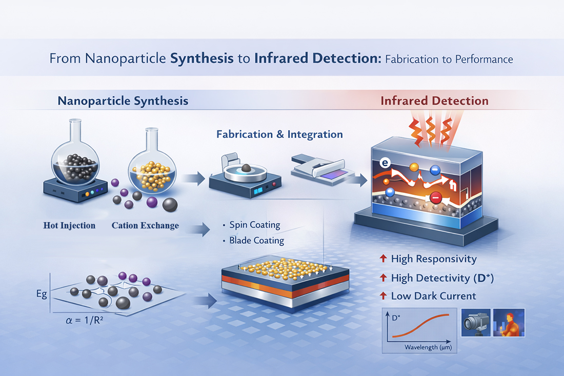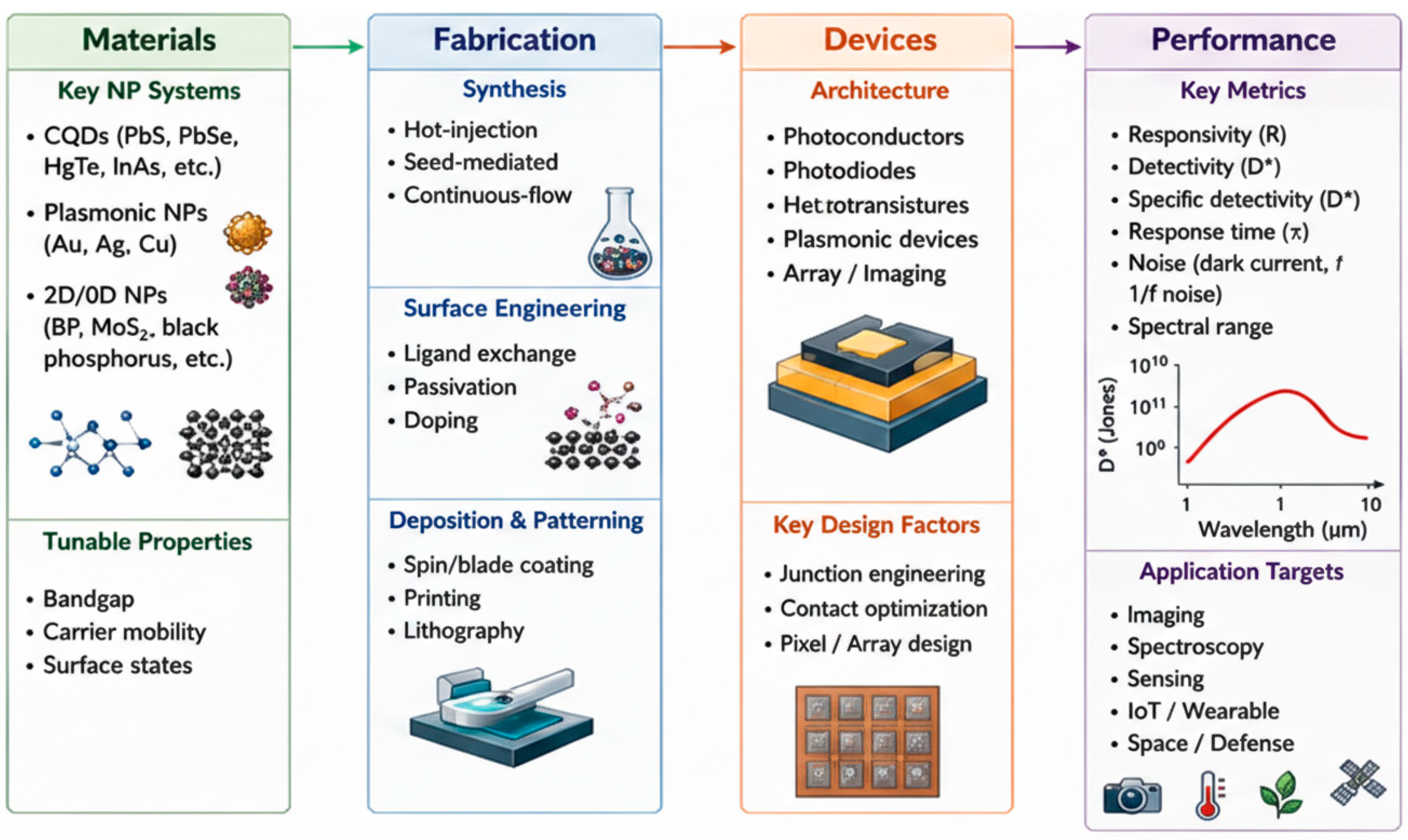




Advances in Nanoparticle-Based Fabrication Techniques for Infrared Detectors: A Comprehensive Review


Abstract
1. Introduction
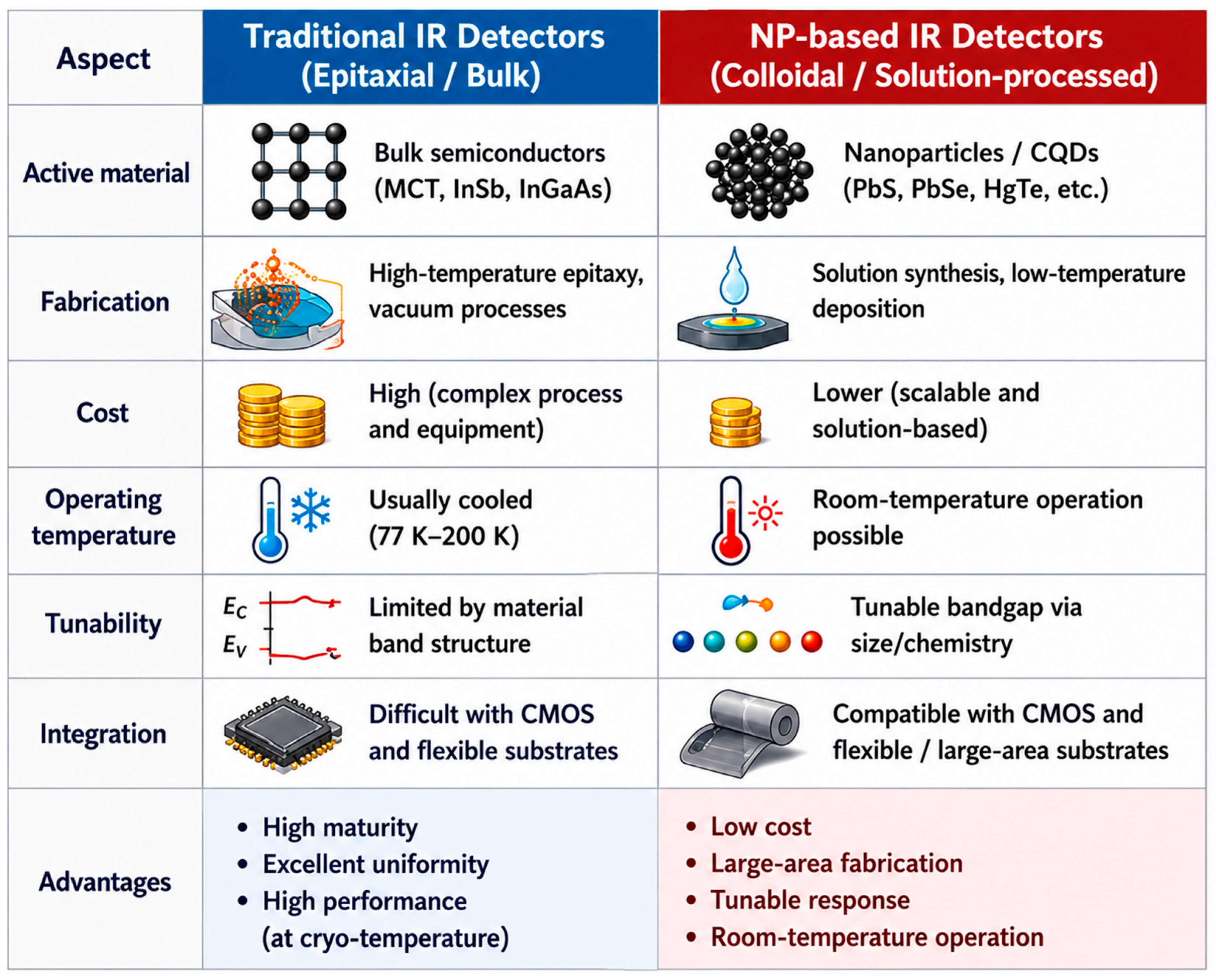
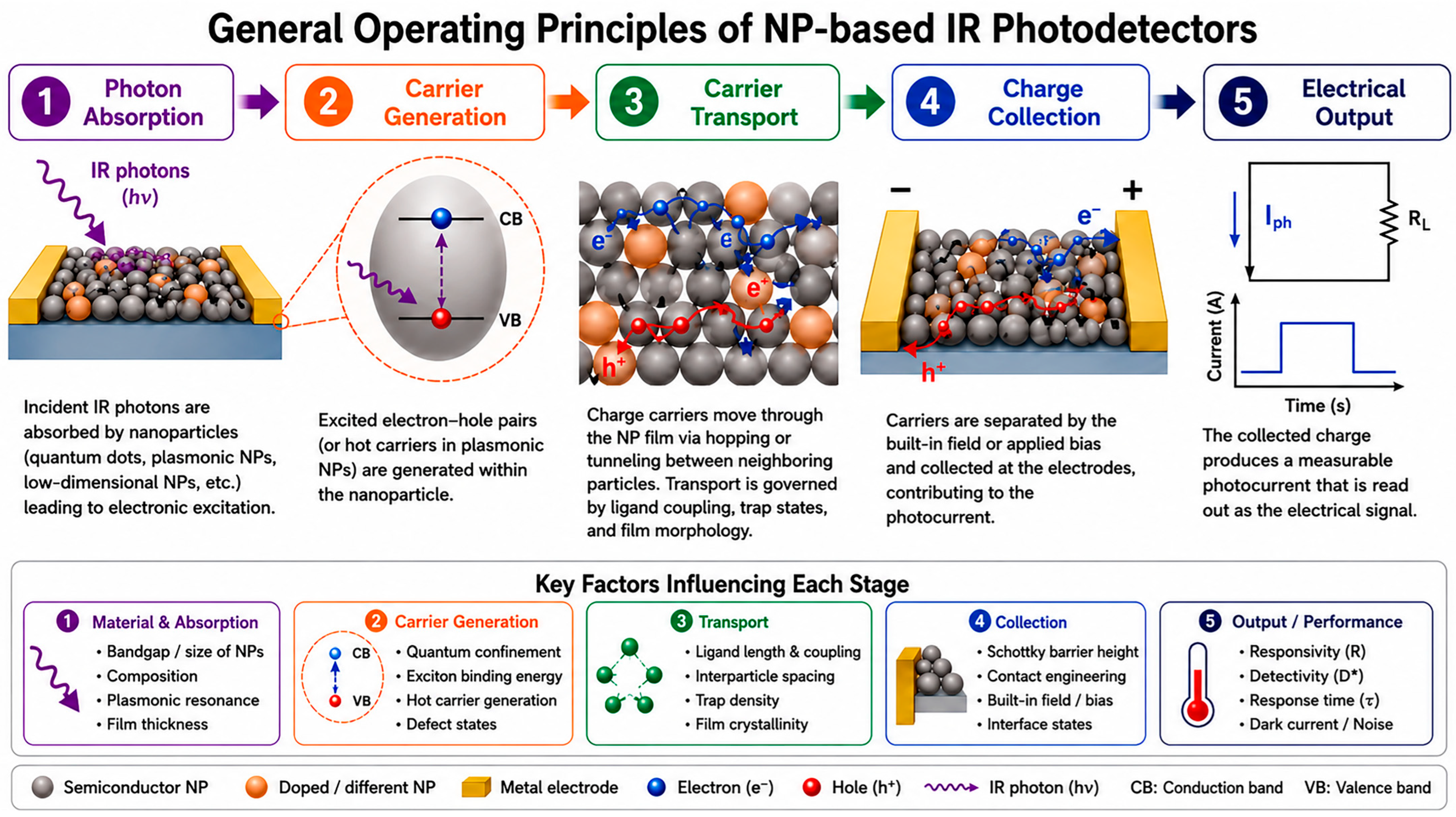
1.1. Overview of Infrared Photodetectors Based on Nanomaterials
1.2. Spectral Selectivity in Nanoparticle-Based IR Photodetectors
1.3. Literature Search and Selection Methodology
2. Key NP Materials Systems: Synthesis, Properties, and Metrics
2.1. Colloidal Quantum Dots (CQDs): Beyond Size Tunability
2.2. Plasmonic Metal NPs: Engineering the Local Field
2.3. Emerging Low-Dimensional and Hybrid Nanostructures
3. Advances in Fabrication and Integration Techniques
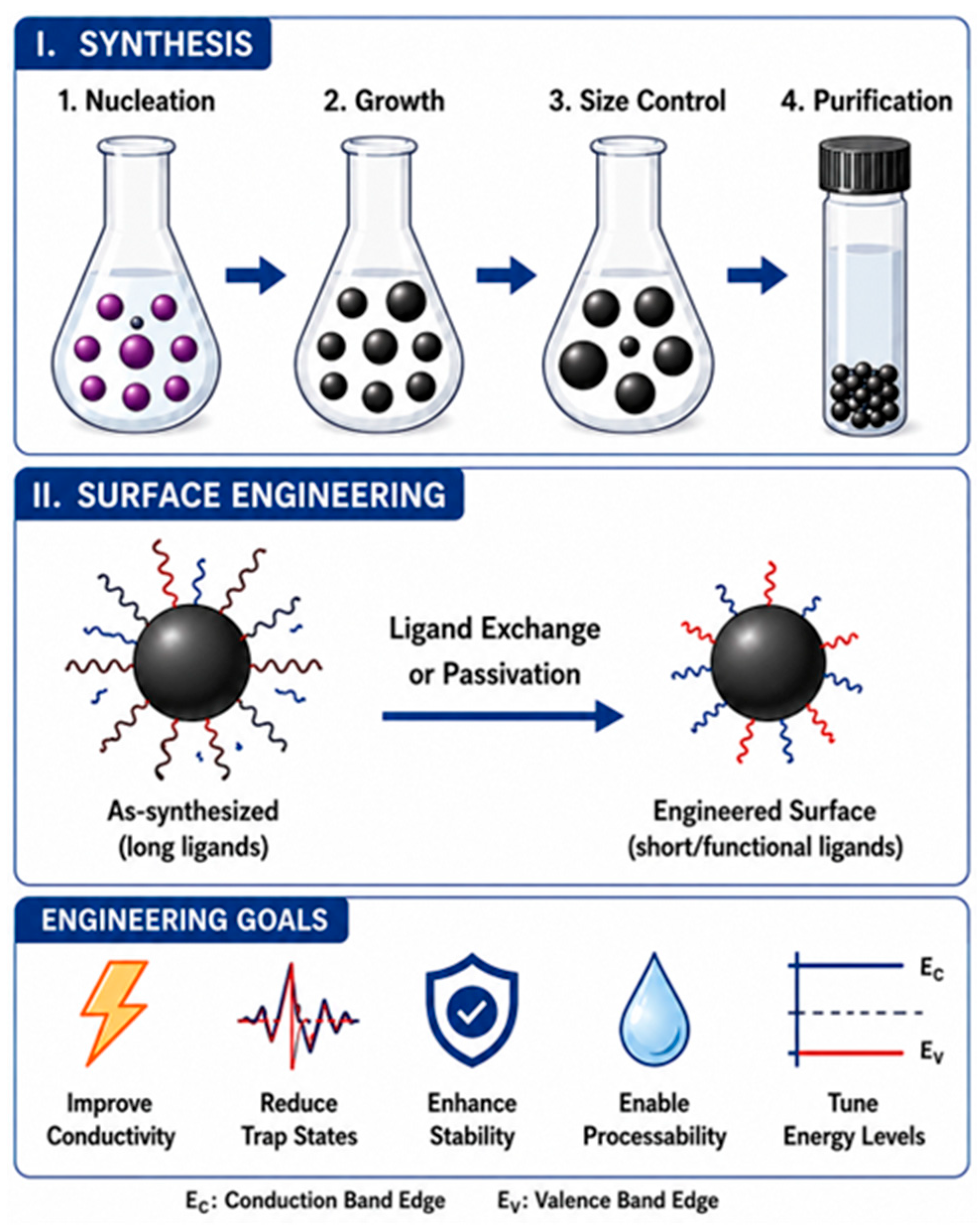
3.1. Synthesis and Surface Engineering: From Lab to Fab
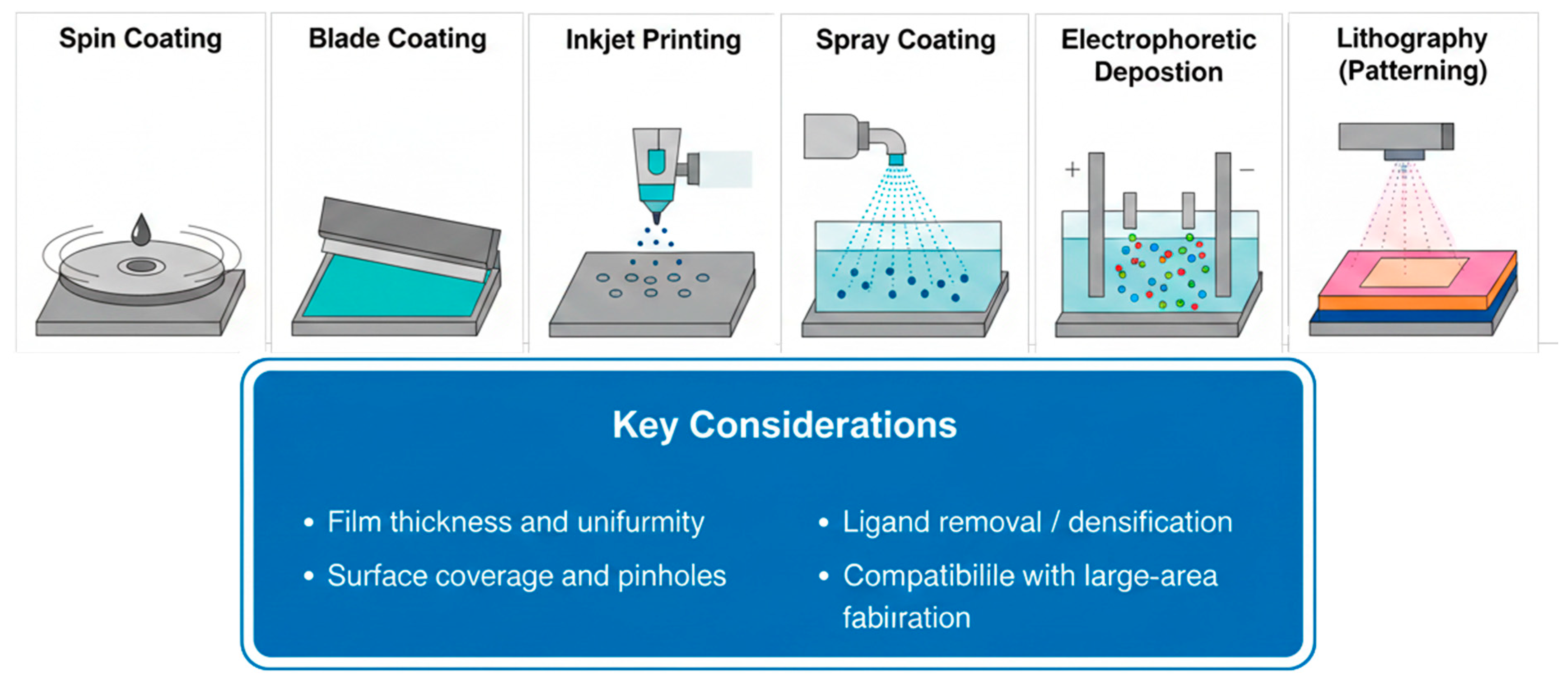
3.2. Deposition and Patterning Techniques: Enabling Large-Area Electronics
- Spin-coating and blade-coating: Remain the conventional techniques for laboratory-scale and proof-of-concept devices. Recent research highlights the importance of solvent engineering and meniscus-guided coating methods to produce more uniform and thicker films [68,69]. For IR absorbers that necessitate thick films (> 500 nm), blade-coating with solvent mixtures (such as octane:butyronitrile) that create a “stick-slip” motion can yield highly uniform, pinhole-free CQD layers, thereby decreasing pixel non-uniformity in arrays to below 5% [70].
- Inkjet printing and 3D aerosol jet printing: Enable digital and additive patterning of NP-based inks, facilitating the monolithic integration of multispectral pixel arrays onto flexible substrates or readout circuits. This marks a significant progress towards the creation of low-cost focal plane arrays (FPAs) [71,72,73]. The capability of aerosol jet printing to concentrate NP aerosol stream allows for the direct writing of CQD patterns with approximately 10 µm linewidth onto pre-patterned Complementary Metal-Oxide-Semiconductor (CMOS) readout integrated circuits (ROICs), which is a crucial advancement towards heterogeneous integration [74].
- Layer-by-Layer (LbL) assembly & electrophoretic deposition (EPD): Provide exceptional control over the thickness and composition of films. EPD, which employs an applied electric field to propel charged NPs to an electrode, is especially effective in forming dense, tightly packed films of large HgTe CQDs for LWIR detection, enhancing packing density by around 30% compared to spin-coating [29,30,75,76,77].
- Spray pyrolysis & electrospray deposition: These are innovative techniques for large-area, conformal coatings. Ultrasonic spray pyrolysis, in which a precursor mist is pyrolyzed on a heated substrate, can deposit high-quality, doped CQD films in a single step, paving the way for direct in situ doping during deposition [78].
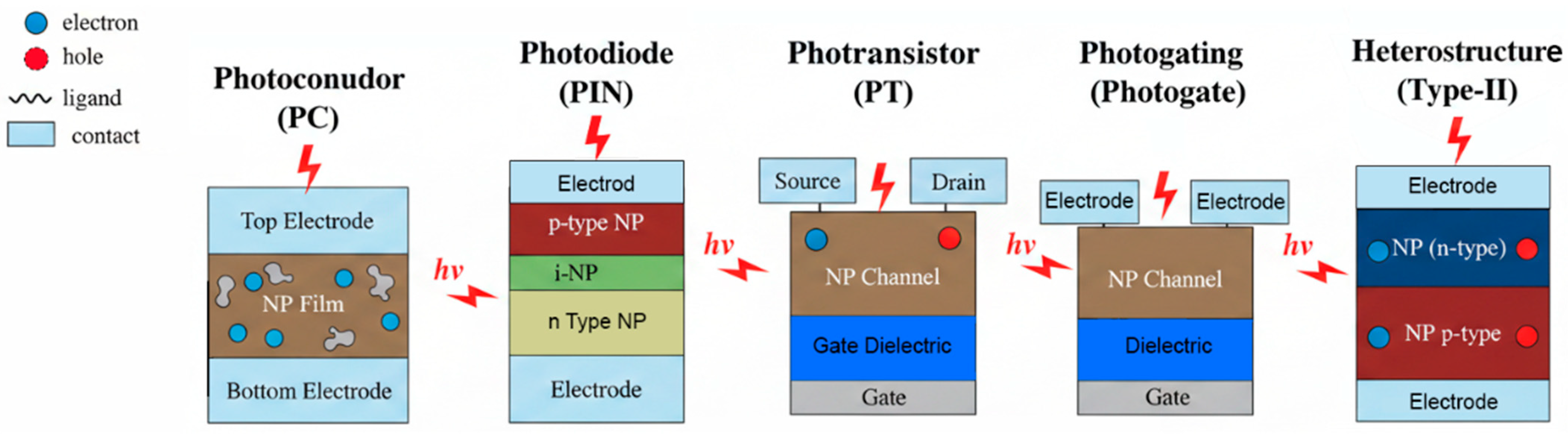
3.3. Device Architecture Innovations: Engineering the Charge Pathway
- Photoconductors: This represents the fundamental architecture. The gain (G) in a photoconductor is expressed as G = τ/τt, where τ denotes the carrier lifetime, and τt signifies the transit time. In films composed of NPs, τ is notably influenced by trap states. By incorporating a minor proportion of reduced graphene oxide (rGO) into a PbS CQD film, percolation pathways for holes can be established, which enhances τ and enables gains exceeding 104, albeit with a reduction in response speed [83].
- Photodiodes: The incorporation of CQD films into p–n or p–i–n junctions leads to a significant decrease in Idark. A key advancement is the implementation of graded heterojunctions, where the size of the CQD (bandgap) is progressively altered throughout the depletion region. This configuration generates a built-in quasi-electric field that facilitates carrier separation, thereby minimizing the reverse bias required for complete depletion and consequently reducing tunneling Idark [84]. Heterojunctions that utilize materials such as graphene or ZnO are the subject of extensive research [85,86,87].
- Plasmon-enhanced and metamaterial detectors: The integration of shaped Au nanorods or nanoantennae with CQD channels leads to significant enhancements in the local field. Metasurfaces, which are periodic arrangements of resonant elements, can be engineered to achieve perfect absorption at a designated IR wavelength within an ultra-thin (< λ/10) CQD layer, significantly improving quantum efficiency without elevating noise levels [88].
- Phototransistors and gate-modulated devices: The use of an NP-based film as the channel material in a field-effect transistor (FET) configuration permits direct control of gain through the gate voltage. PbSe CQD FET photodetectors have shown ultrahigh gain (> 105) and low noise-equivalent power (NEP) by functioning in the subthreshold regime, where the conductivity of the channel is exponentially responsive to changes in photo-induced gate potential [25,26,89,90].
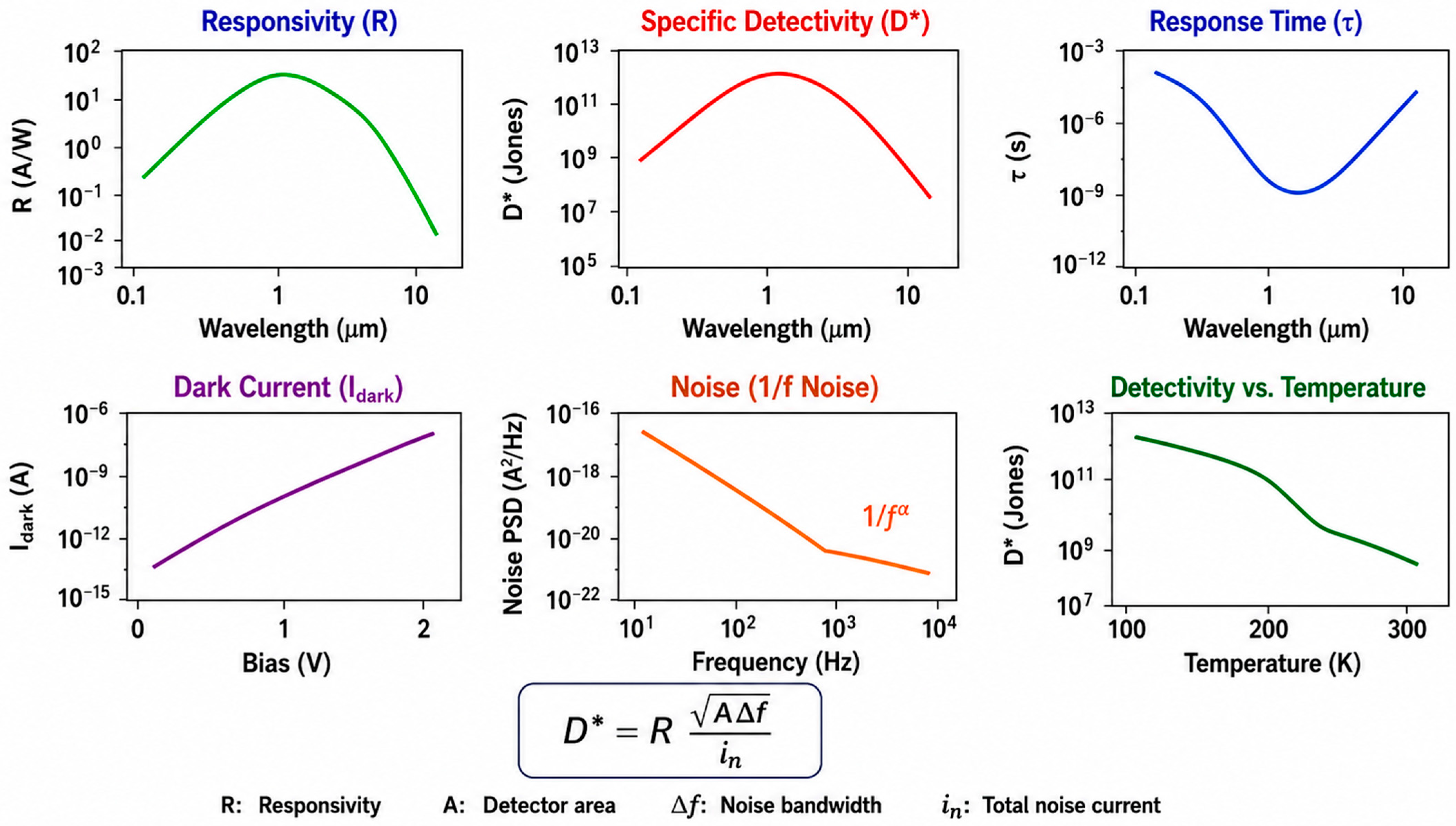
4. Performance Benchmarks, Noise Analysis, and System Integration
5. Critical Challenges, Foundational Limits, and Emerging Frontiers
5.1. Material Stability Beyond Surface Passivation
5.2. Dark Current (Idark) and Noise: Probing the Microscopic Origins
5.3. Charge Transport and Mobility
5.4. Scalability and Uniformity: From Wafers to Webs
5.5. Emerging Frontiers: New Materials and Novel Concepts
5.6. Critical Analysis of Performance Trade-Offs in NP-Based IR Detectors
5.6.1. Gain–Bandwidth Trade-Off in Photoconductive Architectures
5.6.2. Plasmonic Enhancement: Responsivity (R) Versus Detectivity (D*)
5.6.3. Limitations of Hot-Electron Internal Quantum Efficiency
5.6.4. Practical Challenges in Neuromorphic NP-Based IR Detectors
5.7. Environmental, Stability, and Manufacturability Considerations for NP-Based IR Detectors
6. Conclusions and Outlook
Funding
Data Availability Statement
Acknowledgments
Conflicts of Interest
References
- Argirusisyap, N.; Achilleos, A.; Alizadeh, N.; Argirusis, C.; Sourkouni, G. IR Sensors, Related Materials, and Applications. Sensors 2025, 25, 673. [Google Scholar] [CrossRef] [Scilit] [PubMed]
- Bansal, S.; Jain, A.; Kumar, S.; Kumar, P.R.; Prakash, K.; Soliman, M.S.; Islam, M.S.; Islam, M.T. Optoelectronic performance prediction of HgCdTe homojunction photodetector in long wave infrared spectral region using traditional simulations and machine learning models. Sci. Rep. 2024, 14, 28230. [Google Scholar] [CrossRef] [Scilit]
- Sharma, R.; Henderson, L.N.; Sankar, P.; Tresa, M.M.; Oyeku, O.P.; Perez, E.; Thomas, J. Recent Advancements in Nanomaterials for Near-Infrared to Long-Wave Infrared Photodetectors. Adv. Opt. Mater. 2024, 12, 2401821. [Google Scholar] [CrossRef] [Scilit]
- Lim, J.W. Advances in Polymeric Semiconductors for Next-Generation Electronic Devices. Polymers 2025, 17, 3174. [Google Scholar] [CrossRef] [Scilit]
- Kant, K.; Beeram, R.; Cao, Y.; dos Santos, P.S.S.; González-Cabaleiro, L.; García-Lojo, D.; Guo, H.; Joung, Y.; Kothadiya, S.; Lafuente, M.; et al. Plasmonic nanoparticle sensors: Current progress, challenges, and future prospects. Nanoscale Horiz. 2024, 9, 2085–2166. [Google Scholar] [CrossRef] [Scilit] [PubMed]
- Kumar, M.; Seo, H. Ultrafast Photodetectors for Secure Communication, Logic Processing, and Machine Learning-Assisted Optical Material Classification. Adv. Opt. Mater. 2025, 13, e01088. [Google Scholar] [CrossRef] [Scilit]
- Rostami, A.; Dolatyari, M.; Amini, E.; Rasooli, H.; Baghban, H.; Miri, S. Sensitive, Fast, Solution-Processed Ultraviolet Detectors Based on Passivated Zinc Oxide Nanorods. ChemPhysChem 2013, 14, 554–559. [Google Scholar] [CrossRef] [Scilit]
- Robinson, S.; Jia, Y. A Novel Design of MSM Photodetector and the Investigation of Two-Top Contacts Spacing Effects on Detection Speed and Transient Response. Adv. Eng. Intell. Syst. 2022, 1, 82–88. [Google Scholar] [CrossRef]
- Sang, L.; Liao, M.; Sumiya, M. A Comprehensive Review of Semiconductor Ultraviolet Photodetectors: From Thin Film to One-Dimensional Nanostructures. Sensors 2013, 13, 10482–10518. [Google Scholar] [CrossRef] [Scilit]
- Ganesh, K.M.; Bhaskar, S.; Cheerala, V.S.K.; Battampara, P.; Reddy, R.; Neelakantan, S.C.; Reddy, N.; Ramamurthy, S.S. Review of Gold Nanoparticles in Surface Plasmon-Coupled Emission Technology: Effect of Shape, Hollow Nanostructures, Nano-Assembly, Metal–Dielectric and Heterometallic Nanohybrids. Nanomaterials 2024, 14, 111. [Google Scholar] [CrossRef] [Scilit]
- Yan, N.; Qiu, Y.; He, X.; Tang, X.; Hao, Q.; Chen, M. Plasmonic Enhanced Nanocrystal Infrared Photodetectors. Materials 2023, 16, 3216. [Google Scholar] [CrossRef] [Scilit] [PubMed]
- Ilyas, N.; Li, D.; Song, Y.; Zhong, H.; Jiang, Y.; Li, W. Low-Dimensional Materials and State-of-the-Art Architectures for Infrared Photodetection. Sensors 2018, 18, 4163. [Google Scholar] [CrossRef] [Scilit] [PubMed]
- Sargent, E.H. Infrared Quantum Dots. Adv. Mater. 2005, 17, 515. [Google Scholar] [CrossRef] [Scilit]
- Kim, G.; Choi, D.; Eom, S.Y.; Jung, E.D.; Lee, J.H.; Rehl, B.; Kim, S.Y.; Hoogland, S.; Sargent, E.H.; Jeong, K.S. Extended Short-Wavelength Infrared Ink by Surface-Tuned Silver Telluride Colloidal Quantum Dots and Their Infrared Photodetection. ACS Mater. Lett. 2024, 6, 4988–4996. [Google Scholar] [CrossRef] [Scilit]
- Lee, H.K.; Park, T.; Yoo, H. Device Applications Enabled by Bandgap Engineering Through Quantum Dot Tuning: A Review. Materials 2024, 17, 5335. [Google Scholar] [CrossRef] [Scilit] [PubMed]
- Alzakia, F.I.; Tan, S.C. Liquid-Exfoliated 2D Materials for Optoelectronic Applications. Adv. Sci. 2021, 8, 2003864. [Google Scholar] [CrossRef] [Scilit]
- Dolatyari, M.; Rostami, A.; Mathur, S.; Klein, A. UV/IR Dual-Wavelength Photodetector Design Based on ZnO/PMMA/PbSe Nanocomposites. IEEE Trans. Nanotechnol. 2018, 17, 574–581. [Google Scholar] [CrossRef] [Scilit]
- Xiao, B.; Rutherford, G.N.; Sharma, A.P.; Pradhan, S.K.; Bonner, C.E.; Bahoura, M.J. Surface Modification and Charge Injection in a Nanocomposite of Metal Nanoparticles and Semiconductor Oxide Nanostructures. Sci. Rep. 2020, 10, 4743. [Google Scholar] [CrossRef] [Scilit]
- Comanescu, C. Recent Advances in Surface Functionalization of Magnetic Nanoparticles. Coatings 2023, 13, 1772. [Google Scholar] [CrossRef] [Scilit]
- Bae, W.K.; Joo, J.; Padilha, L.A.; Won, J.; Lee, D.C.; Lin, Q.; Koh, W.K.; Luo, H.; Klimov, V.I.; Pietryga, J.M. Highly effective surface passivation of PbSe quantum dots through reaction with molecular chlorine. J. Am. Chem. Soc. 2012, 134, 20160–20168. [Google Scholar] [CrossRef] [Scilit]
- Gurbandurdyyev, B.; Annamuradov, B.; Er, S.B.; Gross, B.; Er, A.O. Advances in Pulsed Liquid-Based Nanoparticles: From Synthesis Mechanism to Application and Machine Learning Integration. Quantum Beam Sci. 2025, 9, 32. [Google Scholar] [CrossRef] [Scilit]
- Gundepudi, K.; Neelamraju, P.M.; Sangaraju, S.; Dalapati, G.K.; Ball, W.B.; Ghosh, S.; Chakrabortty, S. A review on the role of nanotechnology in the development of near-infrared photodetectors: Materials, performance metrics, and potential applications. J. Mater. Sci. 2023, 58, 13889–13924. [Google Scholar] [CrossRef] [Scilit]
- Kinch, M.A. Fundamental physics of infrared detector materials. J. Electron. Mater. 2000, 29, 809–817. [Google Scholar] [CrossRef] [Scilit]
- Bianconi, S.; Mohseni, H. Recent advances in infrared imagers: Toward thermodynamic and quantum limits of photon sensitivity. Rep. Prog. Phys. 2020, 83, 044101. [Google Scholar] [CrossRef] [Scilit]
- Dolatyari, M.; Rostami, A.; Mathur, S.; Klein, A. Trap engineering in solution-processed PbSe quantum dots for high-speed MID-infrared photodetectors. J. Mater. Chem. C 2019, 7, 5658–5669. [Google Scholar] [CrossRef] [Scilit]
- Zhao, X.; Ma, H.; Cai, H.; Wei, Z.; Bi, Y.; Tang, X.; Qin, T. Lead Chalcogenide Colloidal Quantum Dots for Infrared Photodetectors. Materials 2023, 16, 5790. [Google Scholar] [CrossRef] [Scilit]
- Palosz, W.; Trivedi, S.; Jensen, J.L.; Jensen, J. Infrared photoconductive detectors based on PbSe colloidal quantum dots responsive up to 3.3 μm. Opt. Mater. Express 2025, 15, 1214–1223. [Google Scholar] [CrossRef] [Scilit]
- Bugay, C.A.; Caballas, M.C.; Mercado, S.B.; Rubio, J.F.; Serote, P.K.; Villarte, P.N.; Rubi, R.V.C. A Review of Microreactors for Process Intensification. Eng. Proc. 2024, 67, 21. [Google Scholar] [CrossRef] [Scilit]
- Qin, Y.; Guo, T.; Liu, J.; Lin, T.; Wang, J.; Chu, J. Colloidal Quantum Dots in Very-Long-Wave Infrared Detection: Progress, Challenges, and Opportunities. ACS Omega 2023, 8, 19137–19144. [Google Scholar] [CrossRef] [Scilit]
- Yang, J.; Caillas, A.; Feng, J.; Zhang, H.; Shen, X.; Saha, S.; Guyot-Sionnest, P. Long-Wave Infrared HgTe Quantum Dot Photoconductors with Optical Enhancement. ACS Nano 2025, 19, 17874–17883. [Google Scholar] [CrossRef] [Scilit]
- Liu, Z.; Wang, P.; Dong, R.; Gong, W.; Li, J.; Dai, D.; Yan, H.; Zhang, Y. Mid-Infrared HgTe Colloidal Quantum Dots In-Situ Passivated by Iodide. Coatings 2022, 12, 1033. [Google Scholar] [CrossRef] [Scilit]
- Dortaj, H.; Dolatyari, M.; Zarghami, A.; Alidoust, F.; Rostami, A.; Matloub, S.; Yadipour, R. High-speed and high-precision PbSe/PbI2 solution process mid-infrared camera. Sci. Rep. 2021, 11, 1533. [Google Scholar] [CrossRef] [Scilit]
- Siahsar, M.; Jabbarzadeh, F.; Dolatyari, M.; Rostami, G.; Rostami, A. Fabrication of highly sensitive and fast response MIR photodetector based on a new hybrid graphene structure. Sens. Actuators A Phys. 2016, 238, 150–157. [Google Scholar] [CrossRef] [Scilit]
- Safdari, S.; Soltani, M.; Rashedi, G. The effect of inter-dot Coulomb interaction on the charge and energy transport properties of a five-terminal system consisting of three Coulomb-coupled quantum dots. Nanotechnology 2023, 34, 465001. [Google Scholar] [CrossRef] [Scilit]
- Shakhgildyan, G.; Avakyan, L.; Atroshchenko, G.; Vetchinnikov, M.; Zolikova, A.; Ignat’eva, E.; Ziyatdinova, M.; Subcheva, E.; Bugaev, L.; Sigaev, V. Ultra-Broadband Plasmon Resonance in Gold Nanoparticles Precipitated in ZnO-Al2O3-SiO2 Glass. Ceramics 2024, 7, 562–578. [Google Scholar] [CrossRef] [Scilit]
- Mcoyi, M.P.; Mpofu, K.T.; Sekhwama, M.; Mthunzi-Kufa, P. Developments in Localized Surface Plasmon Resonance. Plasmonics 2025, 20, 5481–5520. [Google Scholar] [CrossRef] [Scilit]
- Gu, X.; Timchenko, V.; Heng Yeoh, G.; Dombrovsky, L.; Taylor, R. The Effect of Gold Nanorods Clustering on Near-Infrared Radiation Absorption. Appl. Sci. 2018, 8, 1132. [Google Scholar] [CrossRef] [Scilit]
- Li, Y.; Chen, H.; Zhang, J. Carrier Blocking Layer Materials and Application in Organic Photodetectors. Nanomaterials 2021, 11, 1404. [Google Scholar] [CrossRef] [Scilit]
- Phengdaam, A.; Phetsang, S.; Jonai, S.; Shinbo, K.; Kato, K.; Baba, A. Gold nanostructures/quantum dots for the enhanced efficiency of organic solar cells. Nanoscale Adv. 2024, 6, 3494–3512. [Google Scholar] [CrossRef] [Scilit]
- Xiao, L.; Yan, S.; Chen, T.; Wang, J.; Shi, Y. Enhancing Hot Electron Injection in Plasmonic Photodetectors through Roughened Interfaces. Symmetry 2022, 14, 1628. [Google Scholar] [CrossRef] [Scilit]
- Schuler, S.; Muench, J.E.; Ruocco, A.; Balci, O.; Thourhout, D.V.; Sorianello, V.; Romagnoli, M.; Watanabe, K.; Taniguchi, T.; Goykhman, I.; et al. High-responsivity graphene photodetectors integrated on silicon microring resonators. Nat. Commun. 2021, 12, 3733. [Google Scholar] [CrossRef] [Scilit]
- Jabbarzadeh, F.; Siahsar, M.; Dolatyari, M.; Rostami, G.; Rostami, A. Modification of graphene oxide for applying as mid-infrared photodetector. Appl. Phys. B 2015, 120, 637–643. [Google Scholar] [CrossRef] [Scilit]
- Smith, L.S.; Haidari, H.; Amsalu, A.; Howarth, G.S.; Bryant, S.J.; Walia, S.; Elbourne, A.; Kopecki, Z. Black Phosphorus Nanoflakes: An Emerging Nanomaterial for Clinical Wound Management and Biomedical Applications. Int. J. Mol. Sci. 2024, 25, 12824. [Google Scholar] [CrossRef] [Scilit]
- Alemi, A.; Babalou, A.; Dolatyari, M.; Klein, A.; Meyer, G. Hydrothermal Synthesis of NdIII Doped Bi2Se3 Nanoflowers and their Physical Properties. Z. Anorg. Allg. Chem. 2009, 635, 2053–2057. [Google Scholar] [CrossRef] [Scilit]
- Zhang, M.; Yang, L.; Wu, X.; Wang, J. Black Phosphorus for Photonic Integrated Circuits. Research 2023, 6, 0206. [Google Scholar] [CrossRef] [Scilit]
- Hu, L.; Zhao, Q.; Huang, S.; Zheng, J.; Guan, X.; Patterson, R.; Kim, J.; Shi, L.; Lin, C.H.; Lei, Q.; et al. Flexible and efficient perovskite quantum dot solar cells via hybrid interfacial architecture. Nat. Commun. 2021, 12, 466. [Google Scholar] [CrossRef] [Scilit]
- Wang, Y.P.; Li, H.C.; Huang, Y.C.; Tan, C.S. Synthesis and Applications of Halide Perovskite Nanocrystals in Optoelectronics. Inorganics 2023, 11, 39. [Google Scholar] [CrossRef] [Scilit]
- Bojang, A.A.; Wu, H.-S. Design, Fundamental Principles of Fabrication and Applications of Microreactors. Processes 2020, 8, 891. [Google Scholar] [CrossRef] [Scilit]
- Gariano, G.; Lesnyak, V.; Brescia, R.; Bertoni, G.; Dang, Z.; Gaspari, R.; De Trizio, L.; Manna, L. Role of the Crystal Structure in Cation Exchange Reactions Involving Colloidal Cu2Se Nanocrystals. J. Am. Chem. Soc. 2017, 139, 9583–9590. [Google Scholar] [CrossRef] [Scilit]
- De Trizio, L.; Manna, L. Forging Colloidal Nanostructures via Cation Exchange Reactions. Chem. Rev. 2016, 116, 10852–10887. [Google Scholar] [CrossRef] [Scilit]
- Sajanlal, P.R.; Sreeprasad, T.S.; Samal, A.K.; Pradeep, T. Anisotropic nanomaterials: Structure, growth, assembly, and functions. Nano Rev. 2011, 2, 5883. [Google Scholar] [CrossRef] [Scilit]
- Nath, P.; Ray, A. One-step synthesis of highly fluorescent perovskite nanocrystals in antisolvent for bioimaging. Nano Express 2024, 5, 015016. [Google Scholar] [CrossRef] [Scilit]
- Brutchey, R.L. Diorganyl Dichalcogenides as Useful Synthons for Colloidal Semiconductor Nanocrystals. Acc. Chem. Res. 2015, 48, 2918–2926. [Google Scholar] [CrossRef] [Scilit]
- Deshmukh, S.D.; Ellis, R.G.; Sutandar, D.S.; Rokke, D.J.; Agrawal, R. Versatile Colloidal Syntheses of Metal Chalcogenide Nanoparticles from Elemental Precursors using Amine-Thiol Chemistry. Chem. Mater. 2019, 31, 9087–9097. [Google Scholar] [CrossRef] [Scilit]
- Aqua, J.-N.; Berbezier, I.; Favre, L.; Frisch, T.; Ronda, A. Growth and Self-Organization of SiGe Nanostructures. Phys. Rep. 2013, 522, 59–189. [Google Scholar] [CrossRef] [Scilit]
- Zhang, C.; Han, D.; Zhang, X. PbS Colloidal Quantum Dots: Ligand Exchange in Solution. Coatings 2024, 14, 761. [Google Scholar] [CrossRef] [Scilit]
- Kalluri, A.; Dharmadhikari, B.; Debnath, D.; Patra, P.; Kumar, C.V. Advances in Structural Modifications and Properties of Graphene Quantum Dots for Biomedical Applications. ACS Omega 2023, 8, 21358–21376. [Google Scholar] [CrossRef] [Scilit]
- Belec, B.; Kostevšek, N.; Pelle, G.D.; Nemec, S.; Kralj, S.; Bergant Marušič, M.; Gardonio, S.; Fanetti, M.; Valant, M. Silica Coated Bi2Se3 Topological Insulator Nanoparticles: An Alternative Route to Retain Their Optical Properties and Make Them Biocompatible. Nanomaterials 2023, 13, 809. [Google Scholar] [CrossRef] [Scilit]
- He, H.; Deng, S.; Liu, Y. Environmentally friendly synthesis of quantum dots and their applications in diverse fields from the perspective of environmental compliance: A review. Discov. Nano 2025, 20, 132. [Google Scholar] [CrossRef] [Scilit]
- Hao, Q.; Ma, H.; Xing, X.; Tang, X.; Wei, Z.; Zhao, X.; Chen, M. Mercury Chalcogenide Colloidal Quantum Dots for Infrared Photodetectors. Materials 2023, 16, 7321. [Google Scholar] [CrossRef] [Scilit]
- Sukharevska, N.; Bederak, D.; Goossens, V.M.; Momand, J.; Duim, H.; Dirin, D.N.; Kovalenko, M.V.; Kooi, B.J.; Loi, M.A. Scalable PbS Quantum Dot Solar Cell Production by Blade Coating from Stable Inks. ACS Appl. Mater. Interfaces 2021, 13, 5195–5207. [Google Scholar] [CrossRef] [Scilit]
- Hills-Kimball, K.; Yang, H.; Cai, T.; Wang, J.; Chen, O. Recent Advances in Ligand Design and Engineering in Lead Halide Perovskite Nanocrystals. Adv. Sci. 2021, 8, 2100214. [Google Scholar] [CrossRef] [Scilit]
- Deng, C.; Huang, Q.; Fu, Z.; Lu, Y. Ligand Engineering of Inorganic Lead Halide Perovskite Quantum Dots toward High and Stable Photoluminescence. Nanomaterials 2024, 14, 1201. [Google Scholar] [CrossRef] [Scilit]
- Peng, J.; Chen, Y.; Zhang, X.; Dong, A.; Liang, Z. Solid-State Ligand-Exchange Fabrication of CH3NH3PbI3 Capped PbS Quantum Dot Solar Cells. Adv. Sci. 2016, 3, 1500432. [Google Scholar] [CrossRef] [Scilit]
- You, H.R.; Park, J.Y.; Lee, D.H.; Kim, Y.; Choi, J. Recent Research Progress in Surface Ligand Exchange of PbS Quantum Dots for Solar Cell Application. Appl. Sci. 2020, 10, 975. [Google Scholar] [CrossRef] [Scilit]
- Kloprogge, J.T. X-Ray Photoelectron Spectroscopy (XPS) Study of Layered Double Hydroxides with Different Exchangeable Anions. Appl. Sci. 2025, 15, 1318. [Google Scholar] [CrossRef] [Scilit]
- Al-Amin, K.; Kawsar, M.; Mamun, M.T.R.B.; Sahadat Hossain, M. Fourier transform infrared spectroscopic technique for analysis of inorganic materials: A review. Nanoscale Adv. 2025, 7, 6677–6702. [Google Scholar] [CrossRef] [Scilit]
- Gu, X.; Shaw, L.; Gu, K.; Toney, M.F.; Bao, Z. The meniscus-guided deposition of semiconducting polymers. Nat. Commun. 2018, 9, 534. [Google Scholar] [CrossRef] [Scilit]
- Butt, M.A. Thin-Film Coating Methods: A Successful Marriage of High-Quality and Cost-Effectiveness—A Brief Exploration. Coatings 2022, 12, 1115. [Google Scholar] [CrossRef] [Scilit]
- Fan, J.Z.; Vafaie, M.; Bertens, K.; Sytnyk, M.; Pina, J.M.; Sagar, L.K.; Ouellette, O.; Proppe, A.H.; Rasouli, A.S.; Gao, Y.; et al. Micron Thick Colloidal Quantum Dot Solids. Nano Lett. 2020, 20, 5284–5291. [Google Scholar] [CrossRef] [Scilit]
- Valayil Varghese, T.; Eixenberger, J.; Rajabi-Fakoor, F.; Lazouskaya, M.; Francis, C.; Burgoyne, H.; Wada, K.; Subbaraman, H.; Estrada, D. Multijet Gold Nanoparticle Inks for Additive Manufacturing of Printed and Wearable Electronics. ACS Mater. Au 2023, 4, 65–73. [Google Scholar] [CrossRef] [Scilit]
- Werum, K.; Mueller, E.; Keck, J.; Jaeger, J.; Horter, T.; Glaeser, K.; Buschkamp, S.; Barth, M.; Eberhardt, W.; Zimmermann, A. Aerosol Jet Printing and Interconnection Technologies on Additive Manufactured Substrates. J. Manuf. Mater. Process. 2022, 6, 119. [Google Scholar] [CrossRef] [Scilit]
- Gohel, A.; Gratuze, M.; Ketabi, M.; Izquierdo, R. Direct-Write Printing for Flexible and 3D Electronics: Aerosol Jet vs. Micro Dispensing. Micromachines 2025, 16, 931. [Google Scholar] [CrossRef] [Scilit]
- Ma, T.; Li, Y.; Cheng, H.; Niu, Y.; Xiong, Z.; Li, A.; Jiang, X.; Park, D.; Zhang, K.; Yi, C. Enhanced aerosol-jet printing using annular acoustic field for high resolution and minimal overspray. Nat. Commun. 2024, 15, 6317. [Google Scholar] [CrossRef] [Scilit]
- Punde, A.L.; Shah, S.P.; Hase, Y.V.; Waghmare, A.D.; Shinde, P.S.; Bade, B.R.; Pathan, H.M.; Prasad, M.; Patole, S.P.; Jadkar, S. Self-Biased Photodetector Using 2D Layered Bismuth Triiodide (BiI3) Prepared Using the Spin Coating Method. RSC Adv. 2022, 12, 30157–30166. [Google Scholar] [CrossRef] [Scilit]
- Walker, J.; Koutsos, V. Spin Coating of Silica Nanocolloids on Mica: Self-Assembly of Two-Dimensional Colloid Crystal Structures and Thin Films. Coatings 2023, 13, 1488. [Google Scholar] [CrossRef] [Scilit]
- Falcony, C.; Aguilar-Frutis, M.A.; García-Hipólito, M. Spray Pyrolysis Technique; High-K Dielectric Films and Luminescent Materials: A Review. Micromachines 2018, 9, 414. [Google Scholar] [CrossRef] [Scilit]
- Kim, Y.Y.; Yang, T.Y.; Suhonen, R.; Kemppainen, A.; Hwang, K.; Jeon, N.J.; Seo, J. Roll-to-roll gravure-printed flexible perovskite solar cells using eco-friendly antisolvent bathing with wide processing window. Nat. Commun. 2020, 11, 5146. [Google Scholar] [CrossRef] [Scilit]
- Acosta, C.; Flynn, W.P.; Santillan, L.; Garnsey, S.; Bhalla, A.S.; Guo, R. The Performance Characterization of a Drop-on-Demand Inkjet-Printed Gold Film Under the Temperature Conditions for Airborne Equipment. J. Compos. Sci. 2025, 9, 231. [Google Scholar] [CrossRef] [Scilit]
- Vlnieska, V.; Gilshtein, E.; Kunka, D.; Heier, J.; Romanyuk, Y.E. Aerosol Jet Printing of 3D Pillar Arrays from Photopolymer Ink. Polymers 2022, 14, 3411. [Google Scholar] [CrossRef] [Scilit]
- Boccaccini, A.R.; Keim, S.; Ma, R.; Li, Y.; Zhitomirsky, I. Electrophoretic deposition of biomaterials. J. R. Soc. Interface 2010, 7, S581–S613. [Google Scholar] [CrossRef] [Scilit]
- Saleem, A.; Zhang, Y.; Usman, M.; Haris, M.; Li, P. Tailored architectures of mesoporous carbon nanostructures: From synthesis to applications. Nano Today 2022, 46, 101607. [Google Scholar] [CrossRef] [Scilit]
- Maulu, A.; Navarro-Arenas, J.; Rodríguez-Cantó, P.J.; Sánchez-Royo, J.F.; Abargues, R.; Suárez, I.; Martínez-Pastor, J.P. Charge Transport in Trap-Sensitized Infrared PbS Quantum-Dot-Based Photoconductors: Pros and Cons. Nanomaterials 2018, 8, 677. [Google Scholar] [CrossRef] [Scilit]
- Wang, Y.; Hu, H.; Yuan, M.; Xia, H.; Zhang, X.; Liu, J.; Yang, J.; Xu, S.; Shi, Z.; He, J.; et al. Colloidal PbS Quantum Dot Photodiode Imager with Suppressed Dark Current. ACS Appl. Mater. Interfaces 2023, 15, 58573–58582. [Google Scholar] [CrossRef] [Scilit]
- Haghighatzadeh, A. Z-scheme reduced graphene oxide-ZnO/AgBr nano/hetero-junctions: Modeling of charge transfer mechanism and synergistically improved third-order nonlinear optical responses. Appl. Phys. A 2025, 131, 566. [Google Scholar] [CrossRef] [Scilit]
- Bansal, S.; Kumar, S.; Jain, A.; Rohilla, V.; Prakash, K.; Gupta, A.; Ali, T.; Alenezi, A.M.; Islam, M.S.; Soliman, M.S.; et al. Design and TCAD analysis of few-layer graphene/ZnO nanowires heterojunction-based photodetector in UV spectral region. Sci. Rep. 2025, 15, 7762. [Google Scholar] [CrossRef] [Scilit]
- Jing, C.; Deng, Z.; Cui, H. A Graphene–Molybdenum Disulfide Heterojunction Phototransistor. Crystals 2026, 16, 105. [Google Scholar] [CrossRef] [Scilit]
- Swett, D.W. Near Zero Index Perfect Metasurface Absorber using Inverted Conformal Mapping. Sci. Rep. 2020, 10, 9731. [Google Scholar] [CrossRef] [Scilit]
- Han, J.; Huang, K.; Su, X.; Xiao, X.; Gong, X.; Wang, H.; Cao, J. Carbon Nanotube Transistor with Colloidal Quantum Dot Photosensitive Gate for Ultrahigh External Quantum Efficiency Photodetector. ACS Nano 2023, 17, 9510–9520. [Google Scholar] [CrossRef] [Scilit]
- Adinolfi, V.; Kramer, I.J.; Labelle, A.J.; Sutherland, B.R.; Hoogland, S.; Sargent, E.H. Photojunction field-effect transistor based on a colloidal quantum dot absorber channel layer. ACS Nano 2015, 9, 356–362. [Google Scholar] [CrossRef] [Scilit]
- Yan, N.; Shi, F.; Xue, X.; Zhang, K.; Huo, C.; Chen, M. Cavity-Enhanced Infrared Quantum Dot Homojunction Arrays. Photonics Res. 2025, 13, 1497–1509. [Google Scholar] [CrossRef] [Scilit]
- Zhang, Y.; Hellebusch, D.J.; Bronstein, N.D.; Ko, C.; Ogletree, D.F.; Salmeron, M.; Alivisatos, A.P. Ultrasensitive photodetectors exploiting electrostatic trapping and percolation transport. Nat. Commun. 2016, 7, 11924. [Google Scholar] [CrossRef] [Scilit]
- Wang, H.; Zhou, C.; Li, P.; Yang, L.; Ma, J.; Akaike, R.; Miyake, H.; Xu, H.; Liu, Y. High-sensitivity and fast-response solar-blind photodetectors via band offset engineering for motion tracking. Nat. Commun. 2025, 16, 8175. [Google Scholar] [CrossRef] [Scilit]
- Wei, Y.; Lan, C.; Zhou, S.; Li, C. Recent Advances in Photodetectors Based on Two-Dimensional Material/Si Heterojunctions. Appl. Sci. 2023, 13, 11037. [Google Scholar] [CrossRef] [Scilit]
- Lei, D.; Su, D.; Maier, S.A. New insights into plasmonic hot-electron dynamics. Light Sci. Appl. 2024, 13, 243. [Google Scholar] [CrossRef] [Scilit]
- Zhai, A.; Zhao, C.; Pan, D.; Zhu, S.; Wang, W.; Ji, T.; Li, G.; Wen, R.; Zhang, Y.; Hao, Y.; et al. Organic Photodetectors with Extended Spectral Response Range Assisted by Plasmonic Hot-Electron Injection. Nanomaterials 2022, 12, 3084. [Google Scholar] [CrossRef] [Scilit]
- Li, T.; Wu, H.; Hao, Y.; Ma, F.; Zhu, P.; Li, Z.; Li, F.; Yu, J.; Liu, M.; Lei, C.; et al. High-Performance Broadband Photodetectors Combining Perovskite and Organic Bulk Heterojunction Bifunctional Layers. Crystals 2024, 14, 868. [Google Scholar] [CrossRef] [Scilit]
- Shin, J.; Yoo, H. Photogating Effect-Driven Photodetectors and Their Emerging Applications. Nanomaterials 2023, 13, 882. [Google Scholar] [CrossRef] [Scilit]
- Chen, Y.-T.; Sarangadharan, I.; Sukesan, R.; Hseih, C.-Y.; Lee, G.-Y.; Chyi, J.-I.; Wang, Y.-L. High-field modulated ion-selective field-effect-transistor (FET) sensors with sensitivity higher than the ideal Nernst sensitivity. Sci. Rep. 2018, 8, 8300. [Google Scholar] [CrossRef] [Scilit]
- Bhattarai, K.; Silva, S.; Song, K.; Urbas, A.; Lee, S.J.; Ku, Z.; Zhou, J. Metamaterial Perfect Absorber Analyzed by a Meta-cavity Model Consisting of Multilayer Metasurfaces. Sci. Rep. 2017, 7, 10569. [Google Scholar] [CrossRef] [Scilit]
- Wang, J.; Lang, T.; Hong, Z.; Xiao, M.; Yu, J. Design and Fabrication of a Triple-Band Terahertz Metamaterial Absorber. Nanomaterials 2021, 11, 1110. [Google Scholar] [CrossRef] [Scilit]
- Jin, X.; Zhou, W.; Zhao, Y.; Tian, Q.; Yi, X.; Tao, X.; Craig, A.; Modak, M.; Marshall, A.; Xu, Y.; et al. A Study of the Avalanche Multiplication and Excess Noise in AlxIn1–xAsγSb1–γ Avalanche Photodiodes Lattice-Matched to GaSb. ACS Photonics 2026, 13, 1275–1283. [Google Scholar] [CrossRef] [Scilit]
- Jiang, J.; Jia, J.; Zhao, T.; Liang, K.; Yang, R.; Han, D. Recovery Time of Silicon Photomultiplier with Epitaxial Quenching Resistors. Instruments 2017, 1, 5. [Google Scholar] [CrossRef] [Scilit]
- Pecunia, V.; Anthopoulos, T.D.; Armin, A.; Bouthinon, B.; Caironi, M.; Castellanos-Gomez, A.; Chen, Y.; Cho, K.; Clegg, C.; Fang, X.; et al. Guidelines for Accurate Evaluation of Photodetectors Based on Emerging Semiconductor Technologies. Nat. Photonics 2025, 19, 1178–1188. [Google Scholar] [CrossRef] [Scilit]
- Xia, K.; Gao, X.D.; Fei, G.T.; Xu, S.H.; Liang, Y.F.; Qu, X.X. High-Performance Visible to Mid-Infrared Photodetectors Based on HgTe Colloidal Quantum Dots under Room Temperature. ACS Appl. Mater. Interfaces 2024, 16, 23717–23723. [Google Scholar] [CrossRef] [Scilit]
- Zhang, S.; Hu, Y.; Hao, Q. Advances of Sensitive Infrared Detectors with HgTe Colloidal Quantum Dots. Coatings 2020, 10, 760. [Google Scholar] [CrossRef] [Scilit]
- Xu, Y.; Xue, X.; Wu, L.; Gan, Z.; Chen, M.; Hao, Q. Multiband Infrared Photodetection Based on Colloidal Quantum Dot. Photonics 2026, 13, 89. [Google Scholar] [CrossRef] [Scilit]
- Barthold, P.; Hohls, F.; Maire, N.; Pierz, K.; Haug, R.J. Enhanced shot noise in tunneling through a stack of coupled quantum dots. Phys. Rev. Lett. 2006, 96, 246804. [Google Scholar] [CrossRef] [Scilit]
- Liu, J.; Liu, P.; Shi, T.; Ke, M.; Xiong, K.; Liu, Y.; Chen, L.; Zhang, L.; Liang, X.; Li, H.; et al. Flexible and broadband colloidal quantum dots photodiode array for pixel-level X-ray to near-infrared image fusion. Nat. Commun. 2023, 14, 5352. [Google Scholar] [CrossRef] [Scilit]
- Kwon, J.; Ha, Y.; Choi, S.; Jung, D. Development of a Highly Reliable PbS QDs-Based SWIR Photodetector Based on Metal Oxide Electron/Hole Extraction Layer Formation Conditions. Nanomaterials 2025, 15, 1107. [Google Scholar] [CrossRef] [Scilit]
- Zhou, L.; Huang, Q.; Xia, Y. Plasmon-Induced Hot Electrons in Nanostructured Materials: Generation, Collection, and Application to Photochemistry. Chem. Rev. 2024, 124, 8597–8619. [Google Scholar] [CrossRef] [Scilit]
- Tian, W.; Wang, Y.; Dang, H.; Hou, H.; Xi, Y. Photonic Integrated Circuits: Research Advances and Challenges in Interconnection and Packaging Technologies. Photonics 2025, 12, 821. [Google Scholar] [CrossRef] [Scilit]
- Kazanskiy, N.L.; Khonina, S.N.; Butt, M.A. Advancement in Silicon Integrated Photonics Technologies for Sensing Applications in Near-Infrared and Mid-Infrared Region: A Review. Photonics 2022, 9, 331. [Google Scholar] [CrossRef] [Scilit]
- Mekawey, H.; Elsayed, M.; Ismail, Y.; Swillam, M.A. Optical Interconnects Finally Seeing the Light in Silicon Photonics: Past the Hype. Nanomaterials 2022, 12, 485. [Google Scholar] [CrossRef] [Scilit]
- Du, J.; Zhao, X.; Su, J.; Li, B.; Duan, X.; Dong, T.; Lin, H.; Ren, Y.; Miao, Y.; Radamson, H.H. Review of Short-Wavelength Infrared Flip-Chip Bump Bonding Process Technology. Sensors 2025, 25, 263. [Google Scholar] [CrossRef] [Scilit]
- Xu, K.; Xiao, X.; Zhou, W.; Jiang, X.; Wei, Q.; Chen, H.; Deng, Z.; Huang, J.; Chen, B.; Ning, Z. Inverted Si: PbS Colloidal Quantum Dot Heterojunction-Based Infrared Photodetector. ACS Appl. Mater. Interfaces 2020, 12, 15414–15421. [Google Scholar] [CrossRef] [Scilit]
- Qian, L.; Zhao, X.; Zhang, K.; Huo, C.; Li, Y.; Yan, N.; Shi, F.; Peng, X.; Chen, M. Si-HgTe Quantum Dot Visible-Infrared Photodetector. Nanomaterials 2025, 15, 262. [Google Scholar] [CrossRef] [Scilit]
- Wang, L.; He, S.J.; Wang, K.Y.; Luo, H.H.; Hu, J.G.; Yu, Y.Q.; Xie, C.; Wu, C.Y.; Luo, L.B. Dual-plasmonic Au/graphene/Au-enhanced ultrafast, broadband, self-driven silicon Schottky photodetector. Nanotechnology 2018, 29, 505203. [Google Scholar] [CrossRef] [Scilit]
- Sun, Z.; Liu, Z.; Li, J.; Tai, G.A.; Lau, S.P.; Yan, F. Infrared photodetectors based on CVD-grown graphene and PbS quantum dots with ultrahigh responsivity. Adv. Mater. 2012, 24, 5878–5883. [Google Scholar] [CrossRef] [Scilit]
- Saleem, M.I.; Yang, S.; Batool, A.; Sulaman, M.; Veeramalai, C.P.; Jiang, Y.; Tang, Y.; Cui, Y.; Tang, L.; Zou, B. CsPbI3 Nanorods as the Interfacial Layer for High-Performance, All-Solution-Processed Self-Powered Photodetectors. J. Mater. Sci. Technol. 2021, 75, 196–204. [Google Scholar] [CrossRef] [Scilit]
- Xue, X.; Hao, Q.; Chen, M. Very Long Wave Infrared Quantum Dot Photodetector up to 18 μm. Light Sci. Appl. 2024, 13, 89. [Google Scholar] [CrossRef] [Scilit]
- Kundu, B.; Özdemir, O.; Dalmases, M.; Kumar, G.; Konstantatos, G. Hybrid 2D-QD MoS2-PbSe Quantum Dot Broadband Photodetectors with High-Sensitivity and Room-Temperature Operation at 2.5 μm. Adv. Opt. Mater. 2021, 9, 2101378. [Google Scholar] [CrossRef] [Scilit]
- Vale, B.R.C.; Silva, F.O.; Carvalho, M.S.; Raphael, E.; Ferrari, J.L.; Schiavon, M.A. Water-Soluble CdTe/CdS Core/Shell Semiconductor Nanocrystals: How Their Optical Properties Depend on the Synthesis Methods. Crystals 2016, 6, 133. [Google Scholar] [CrossRef] [Scilit]
- Xue, X.; Chen, M.; Luo, Y.; Qin, T.; Tang, X.; Hao, Q. High-Operating-Temperature Mid-Infrared Photodetectors via Quantum Dot Gradient Homojunction. Light Sci. Appl. 2023, 12, 2. [Google Scholar] [CrossRef] [Scilit]
- Mazzaro, R.; Piccioni, A.; Salvi, M.; Vecchi, P.; Mazzanti, M.; Caramori, S.; Boscherini, F.; Pasquini, L. Operando x-ray absorption spectroscopy unveils light-driven redox dynamics at the semiconductor/cocatalyst interface. Sci. Adv. 2025, 11, eadx8089. [Google Scholar] [CrossRef] [Scilit]
- Racko, J.; Mikolášek, M.; Granzner, R.; Breza, J.; Donoval, D.; Grmanová, A.; Harmatha, L.; Schwierz, F.; Fröhlich, K. Trap-assisted tunnelling current in MIM structures. Cent. Eur. J. Phys. 2011, 9, 230–241. [Google Scholar] [CrossRef] [Scilit]
- Li, W.G.; Wang, X.D.; Feng, L.J.; Wei, Z.F.; Xu, Y.F.; Chen, H.Y.; Kuang, D.B. A Laminar MAPbBr3/MAPbBr3−xIx Graded Heterojunction Single Crystal for Enhancing Charge Extraction and Optoelectronic Performance. J. Mater. Chem. C 2019, 7, 5670–5676. [Google Scholar] [CrossRef] [Scilit]
- Tamersit, K.; Ramezani, Z.; Amiri, I.S. Improved performance of sub-10-nm band-to-band tunneling n-i-n graphene nanoribbon field-effect transistors using underlap engineering: A quantum simulation study. J. Phys. Chem. Solids 2022, 160, 110312. [Google Scholar] [CrossRef] [Scilit]
- Kumar, J.; Shrivastava, M. Role of Chalcogen Defect Introducing Metal-Induced Gap States and Its Implications for Metal-TMDs’ Interface Chemistry. ACS Omega 2023, 8, 10176–10184. [Google Scholar] [CrossRef] [Scilit]
- Cuadra, L.; Salcedo-Sanz, S.; Nieto-Borge, J.C. Carrier Transport in Colloidal Quantum Dot Intermediate Band Solar Cell Materials Using Network Science. Int. J. Mol. Sci. 2023, 24, 3797. [Google Scholar] [CrossRef] [Scilit]
- Heyne, B.; Arlt, K.; Geßner, A.; Richter, A.F.; Döblinger, M.; Feldmann, J.; Taubert, A.; Wedel, A. Mixed Mercaptocarboxylic Acid Shells Provide Stable Dispersions of InPZnS/ZnSe/ZnS Multishell Quantum Dots in Aqueous Media. Nanomaterials 2020, 10, 1858. [Google Scholar] [CrossRef] [Scilit]
- Liang, X.; Liu, H.; Fujinami, S.; Ito, M.; Nakajima, K. Simultaneous Visualization of Microscopic Conductivity and Deformation in Conductive Elastomers. ACS Nano 2024, 18, 3438–3446. [Google Scholar] [CrossRef] [Scilit]
- Duarte, V.C.M.; Andrade, L. Recent Advancements on Slot-Die Coating of Perovskite Solar Cells: The Lab-to-Fab Optimisation Process. Energies 2024, 17, 3896. [Google Scholar] [CrossRef] [Scilit]
- Khayal, A.; Dawane, V.; Amin, M.A.; Tirth, V.; Yadav, V.K.; Algahtani, A.; Khan, S.H.; Islam, S.; Yadav, K.K.; Jeon, B.-H. Advances in the Methods for the Synthesis of Carbon Dots and Their Emerging Applications. Polymers 2021, 13, 3190. [Google Scholar] [CrossRef] [Scilit]
- Bi, S.; Wang, R.; Han, X.; Wang, Y.; Tan, D.; Shi, B.; Jiang, C.; He, Z.; Asare-Yeboah, K. Recent Progress in Electrohydrodynamic Jet Printing for Printed Electronics: From 0D to 3D Materials. Coatings 2023, 13, 1150. [Google Scholar] [CrossRef] [Scilit]
- Mishra, A.; Aghaee, M.; Tamer, I.M.; Budman, H. Spectroscopic Advances in Real Time Monitoring of Pharmaceutical Bioprocesses: A Review of Vibrational and Fluorescence Techniques. Spectrosc. J. 2025, 3, 12. [Google Scholar] [CrossRef] [Scilit]
- Xia, P.; Wang, S.; Chen, Y.; Gulsaran, A.; Zhang, Y.; Vafaie, M.; Imran, M.; Najarian, A.M.; Liu, Y.; Ban, H.; et al. Improved Facet and Edge Passivation in Near-Infrared III-V Colloidal Quantum Dot Photodetectors. Adv. Mater. 2025, 37, 2419020. [Google Scholar] [CrossRef] [Scilit]
- Ju, M.G.; Dai, J.; Ma, L.; Zhou, Y.; Zeng, X.C. AgBiS2 as a low-cost and eco-friendly all-inorganic photovoltaic material: Nanoscale morphology-property relationship. Nanoscale Adv. 2019, 2, 770–776. [Google Scholar] [CrossRef] [Scilit]
- Zeiske, S.; Ban, H.W.; Li, X.; Deng, B.; López-Arteaga, R.; Kazianga, U.H.; Han, M.G.; Kim, T.-G.; Chen, B.; Sargent, E.H. Revealing Additional Size-Dependent Defect Suppression Channels Governing Detectivity in InAs Colloidal Quantum Dot Photodiodes. Nano Lett. 2025, 25, 16862–16868. [Google Scholar] [CrossRef] [Scilit]
- Maietta, I.; Otero-Martínez, C.; Fernández, S.; Sánchez, L.; González-Fernández, Á.; Polavarapu, L.; Simón-Vázquez, R. The Toxicity of Lead and Lead-Free Perovskite Precursors and Nanocrystals to Human Cells and Aquatic Organisms. Adv. Sci. 2025, 12, e2415574. [Google Scholar] [CrossRef] [Scilit]
- Sun, Z.; Zhao, X.; Si, H.; Liao, Q.; Zhang, Y. Biomimetic Synapses Based on Halide Perovskites for Neuromorphic Vision Computing: Materials, Devices, and Applications. Nano-Micro Lett. 2026, 18, 246. [Google Scholar] [CrossRef] [Scilit]
- De Boer, J.J.; Alvarez, A.O.; Schmidt, M.C.; Ehrler, B. In-sensor computing with halide perovskite-based optoelectronic reservoir networks. Device 2026, 4, 101000. [Google Scholar] [CrossRef] [Scilit]
- Yi, H.; Zhou, M.; Xie, H.; Chen, B.; Wang, Y.; Liu, F.; Shen, J.; Shen, J. Physics-Driven Computational Multispectral Imaging for Accurate Color Measurement. Sensors 2025, 25, 5443. [Google Scholar] [CrossRef] [Scilit]
- Bu, Y.; Ye, T.; Wang, R.; Zhou, J.; Deng, J.; Zhen, Y.; Shi, M.; Jing, W.; Xin, R.; Zhang, Y.; et al. High discrimination infrared polarimetry via intrinsic anisotropic photogating in black phosphorus meta-polarization detectors. Nat. Commun. 2025, 16, 10137. [Google Scholar] [CrossRef] [Scilit]
- Han, J.; Fu, Z.; Wei, J.; Han, S.; Deng, W.; Hu, F.; Wang, Z.; Zhou, H.; Yu, H.; Gou, J.; et al. 2D materials-based next-generation multidimensional photodetectors. Light Sci. Appl. 2025, 14, 362. [Google Scholar] [CrossRef] [Scilit]
- Gao, J.; Wang, Z.; Tang, Y.; Han, J.; Gao, M.; Wu, J.; Chen, Q.; Yu, D.; Wang, E.; Zhu, F. Mitigating Dark Current in Photomultiplication Organic Photodetectors via the Charge Trap Gradient Bulk Heterojunction. ACS Appl. Mater. Interfaces 2025, 17, 52426–52434. [Google Scholar] [CrossRef] [Scilit]
- Li, P.; Lu, Z.-H. Interface Engineering in Organic Electronics: Energy-Level Alignment and Charge Transport. Small Sci. 2020, 1, 2000015. [Google Scholar] [CrossRef] [Scilit]
- Jeong, T.-J.; Yu, X.; Harris, T.A.L. Scaled Production of Functionally Gradient Thin Films Using Slot Die Coating on a Roll-to-Roll System. ACS Appl. Mater. Interfaces 2024, 16, 9264–9274. [Google Scholar] [CrossRef] [Scilit]
- Shi, W.; Guo, R.; Tian, G.; Zhang, W.; Chen, Y.; Wang, W.; Wang, Y.; Cui, D.; Wen, J.; Liu, D.; et al. Self-powered Ag2Se/SiO2/Si heterojunctions for ultrafast broadband high-sensitivity photodetection. Chem. Eng. J. 2025, 520, 166076. [Google Scholar] [CrossRef] [Scilit]
- Wang, F.; Fang, S.; Zhang, Y.; Wang, Q.J. 2D computational photodetectors enabling multidimensional optical information perception. Nat. Commun. 2025, 16, 6791. [Google Scholar] [CrossRef] [Scilit]
- Ma, J.; Yang, S.; Yang, Z.; He, Z.; Du, Z. Functional Nanomaterials for Advanced Bioelectrode Interfaces: Recent Advances in Disease Detection and Metabolic Monitoring. Sensors 2025, 25, 4412. [Google Scholar] [CrossRef] [Scilit]
- Rogalski, A.; Hu, W.; Wang, F.; Martyniuk, P. Performance of Low-Dimensional Solid Room-Temperature Photodetectors: Critical View. Materials 2024, 17, 4522. [Google Scholar] [CrossRef] [Scilit]
- Baskoutas, S. Advanced Nanomaterials for Quantum Technology, Sensor and Health Therapy Applications. Nanomaterials 2023, 13, 1506. [Google Scholar] [CrossRef] [Scilit]
- Kong, L.; Wang, S.; Su, Q.; Liu, Z.; Liao, G.; Sun, B.; Shi, T. Printed Two-Dimensional Materials for Flexible Photodetectors: Materials, Processes, and Applications. Sensors 2025, 25, 1042. [Google Scholar] [CrossRef] [Scilit]
- Huang, Y.T.; Nodari, D.; Furlan, F.; Zhang, Y.; Rusu, M.; Dai, L.; Andaji-Garmaroudi, Z.; Darvill, D.; Guo, X.; Rimmele, M.; et al. Fast Near-Infrared Photodetectors Based on Nontoxic and Solution-Processable AgBiS2. Small 2024, 20, 2310199. [Google Scholar] [CrossRef] [Scilit]
- Li, Z.; Han, H.; Chao, L.; Chen, Y.; Chen, G.; Huang, W. Recent Advances of AgBiS2: Synthesis Methods, Photovoltaic Device, Photodetector, and Sensors. Electromag. Sci. 2025, 3, 0090451. [Google Scholar] [CrossRef] [Scilit]
- Feng, W.; Qin, T.; Tang, X. Advances in Infrared Detectors for In-Memory Sensing and Computing. Photonics 2024, 11, 1138. [Google Scholar] [CrossRef] [Scilit]
- Tang, Q.; Zhong, F.; Li, Q.; Weng, J.; Li, J.; Lu, H.; Wu, H.; Liu, S.; Wang, J.; Deng, K.; et al. Infrared Photodetection from 2D/3D van der Waals Heterostructures. Nanomaterials 2023, 13, 1169. [Google Scholar] [CrossRef] [Scilit]
- Zha, J.; Luo, M.; Ye, M.; Ahmed, T.; Yu, X.; Lien, D.-H.; He, Q.; Lei, D.; Ho, J.C.; Bullock, J.; et al. Infrared Photodetectors Based on 2D Materials and Nanophotonics. Adv. Funct. Mater. 2022, 32, 2111970. [Google Scholar] [CrossRef] [Scilit]



| Synthesis Strategy | Principle | Representative Materials | Key Advantages | Main Limitations | Typical Feature Size | Typical Applications | Refs. |
|---|---|---|---|---|---|---|---|
| Hot-Injection | rapid precursor injection at elevated temperature to separate nucleation and growth | PbS, PbSe, CsPbX3 | excellent size control; high crystallinity | batch-to-batch variation; precursor sensitivity | 2–10 nm | CQD photodiodes, SWIR detectors | [25,26,47] |
| Continuous-Flow/Microreactor | flow-based synthesis with controlled residence time and heat transfer | PbS | scalable; reproducible; precise thermal control | more complex equipment | 3–8 nm | large-scale CQD production | [48] |
| Cation Exchange | partial/complete ion replacement in preformed nanocrystals | PbSe, CdSe, Cu2Se | enables composition tuning and heterostructures | surface defects may form | Tunable | bandgap engineering; heterojunction devices | [25,26,49,50] |
| Solvothermal/Hydrothermal | high-pressure reaction in sealed reactor | Bi2Se3, BP nanosheets | simple processing; ligand-free synthesis | broader size distribution | 5–100 nm | broadband IR absorbers | [43,44] |
| Seed-Mediated Growth | controlled growth on pre-existing seeds | Au, Ag | shape and aspect-ratio control | complex growth kinetics | aspect ratio 2–10 | plasmonic IR structures | [51] |
| Ligand-Assisted Precipitation | rapid crystallization using precursor–antisolvent interaction | Perovskite nanocrystals | low-temperature and scalable | limited monodispersity | 3–15 nm | solution-processed photodetectors | [52] |
| Colloidal Synthesis via Metal Chalcogenide Precursors | controlled reaction of metal and chalcogen precursors | PbS, AgBiS2 | improved stoichiometry and reduced defects | higher precursor cost | 4–10 nm | high-quality CQD films | [53,54] |
| Epitaxial Nanostructure Growth (SK/VW/FM) | strain- or surface-driven crystal growth on lattice-engineered substrates | Ge/Si QDs, GeSiSn QDs, III–V QDs | excellent crystallinity; low defect density; precise interfaces; CMOS compatibility | high equipment cost; limited throughput; thermal constraints | self-assembled QDs (typically 5–50 nm) | Si-compatible IR photodiodes, QD detectors, integrated photonics | [55] |
| Material | Type | Tunable Range (µm) | Key Advantages | Key Challenges | Primary Synthesis Route | Typical Mobility (cm2/V·s) | Performance record (D*, Jones) | Refs. |
|---|---|---|---|---|---|---|---|---|
| PbS/PbX2 CQDs | semiconductor | 0.8–4.0 | good tunability, high absorption | surface traps, ligand resistivity | hot-injection | 10−2–101 | > 1013 at 1.55 µm, 300 K | [56] |
| HgTe CQDs | semiconductor | 3–12 | room-T VLWIR operation | oxidation, stability | modified hot-injection | 10−3–10−1 | 2 × 10¹⁰ at 5 µm, 300 K | [29,30,31] |
| Au/Ag NPs | plasmonic metal | 1–10 | strong LSPR, ultrafast response | low R, cost | seed-mediated growth | N/A (Metal) | N/A (speed <100 fs) | [35,37,40] |
| Graphene QDs | 2D | < 10 | high mobility, flexibility | low absorption | top-down etching | ~102 | 1011 at 1.5 µm, 300 K | [42,57] |
| BP nanosheets | 2D semiconductor | 1–8 | anisotropy, high mobility | ambient instability | liquid exfoliation | 102–103 | 1011 at 3.4 µm, 300 K | [43,45] |
| CsPbX3 nanocrystals | perovskite | < 1.8 | high defect tolerance, fast response | ion migration, thermal stability | ligand-assisted reprecipitation, hot-injection | 10−4–10−2 | 109 at 1.5 µm, 300 K | [47] |
| Bi2Se3 NPs | topological insulator | 2–8 | topological surface states | complex synthesis, impurities | coll. synthesis | N/A | 109 at 4 µm, 300 K | [58] |
| Method | Principle | Scalability | Film Uniformity | Resolution | Throughput | Best For | Refs. |
|---|---|---|---|---|---|---|---|
| Spin-Coating | centrifugal force | lab-scale | high (thin) | wafer-scale | high | R&D, test structures | [76,77] |
| Blade/Bar-Coating | meniscus guidance | pilot-line | excellent (thick) | mm scale | very high | large-area flexible substrates | [78] |
| Inkjet Printing | drop-on-demand | high | moderate | 20–50 µm | medium | multispectral pixel patterning | [71,72,73,74,79] |
| Aerosol Jet Printing | focused aerosol stream | high | good | ~10 µm | medium | direct write on 3D/CMOS | [74,80] |
| Electrophoretic Deposition (EPD) | electric field-driven | medium | very high (dense) | electrode-defined | medium | dense LWIR films | [81] |
| Spray Pyrolysis | in situ reaction from the mist | high | moderate | cm scale | high | conformal, doped films | [77,82] |
| Architecture | Operating Mechanism | Key Metrics | Selectivity Mechanism | Advantages | Key Challenges/Noise Mechanism | Refs. |
|---|---|---|---|---|---|---|
| Photoconductor | conductivity modulation | R, gain, NEP | bandgap-controlled absorption | simple, high gain | high 1/f noise, low speed | [16,92] |
| Photodiode (p–i–n) | built-in field separation | D*, R, EQE, Idark | junction + optical cavity | low noise, fast, photovoltaic | complex fabrication, interface traps | [93,94] |
| Plasmonic Hot-Electron | hot carrier injection | τ, ηIQE | resonance wavelength | ultrafast, sub-bandgap | very low ηIQE, thermal noise | [95,96] |
| Hybrid Heterojunction | band alignment engineering | R, spectral range | band alignment | broadband, multifunctional | interface recombination | [46,97] |
| Phototransistor (FET) | gate-modulated conductivity | gain, NEP, specific detectivity | gate-tunable spectral response | tunable gain, very high sensitivity | gate hysteresis, stability | [98,99] |
| Metamaterial Absorber | resonant cavity enhancement | absorption %, Q-factor | resonant spectral filtering | near-unity absorption in an ultra-thin layer | narrowband, complex fabrication | [100,101] |
| Avalanche Photodiode (APD) | impact ionization and internal carrier multiplication under reverse bias | gain (M), D*, bandwidth, excess noise factor | primarily determined by absorber bandgap and optical filtering a | internal gain, high sensitivity, fast detection | Multiplication noise, high bias voltage, temperature sensitivity | [102] |
| Single-Photon Avalanche Diode (SPAD)/Silicon Photomultiplier (SiPM) | Geiger-mode avalanche triggering from single-photon events | photon detection efficiency (PDE), timing jitter, dark count rate | defined by absorber spectral response b | single-photon sensitivity, ultralow signal detection | afterpulsing, dark counts, dead time | [103] |
| Material/Structure | Spectral Range (µm) | Peak Wavelength (µm) | D* (Jones) a | R (A/W) | Bias Voltage (V) | Operation T (K) | Response Time | Architecture | Ref. |
|---|---|---|---|---|---|---|---|---|---|
| PbS CQD Photodiode | 1–2 | 1.54 | > 1011 | 0.2–1.2 | −0.5 | 300 | µs | p–n on Si heterojunction | [116] |
| HgTe CQD Photodiode | < 2.8 | 1.55 | 1011 | 0.24 | 0.6 | 300 | µs | p–i–n on Si | [117] |
| Au/graphene/Au | < 1.33 | 1.33 | 2.4 × 10¹³ | 10−3 | 0 | 300 | 360 ns | plasmonic Schottky | [118] |
| Graphene–PbS CQD Hybrid | 1.45–1.59 | 1.55 | 1010 | 107 | 5 | 300 | Ms | photoconductor | [119] |
| CsPbI3/PbS | < 1.7 | 1.55 | 4.5 × 10¹³ | 11.12 | 0.53 | 300 | Ms | bulk heterojunction | [120] |
| Modified HgTe CQD | 8–18 | 18 | 6.6 × 10⁸ | 0.3 | 3 | 80 | µs | MSM-photoconductor | [121] |
| PbSe-MoS2 | 2–3 | 3 | 7.7 × 10¹⁰ | 137.6 | 1 | 300 | Ms | broadband absorber | [122] |
| HgTe CQD Homojunc. array with Fabry–Perot Cavity | 1.4–2.5 | 2.5 | 4.64 × 10¹¹ | 0.54 | 1 | 300 | µs | 56-channel CQD spectrometer array | [123] |
| Challenge Category | Specific Issue | Current Mitigation Strategies | Performance Impact | Key Research Needs | Refs. |
|---|---|---|---|---|---|
| Material stability | oxidation, ligand desorption, and ion migration (perovskites) | inorganic shells, cross-linked ligands, and ALD encapsulation | extends operational lifetime from h to > 1000 h | in operando degradation studies; predictive stability models | [144,145] |
| Electronic noise | high Idark, 1/f noise, trap-assisted tunneling | graded heterojunctions, bulk barriers, trap-passivating ligands | reduces Idark by 2–3 orders of magnitude; lowers NEP | correlated noise-defect spectroscopy; DFT modeling of trap states | [146] |
| Charge transport | low mobility, energetic disorder | atomic/mixed ligand exchange, doping, energy-level alignment | increases μ (mobility) from 10−3 to > 10 cm2/V·s | nanoscale mapping of transport | [147] |
| Scalability | film non-uniformity, low throughput, and pattern resolution | slot-die/blade coating, electrohydrodynamic printing, convergent synthesis | enables uniform films > 100 cm2; < 5% pixel variation | in-line metrology; roll-to-roll process integration | [148] |
| Next-gen. materials | Pb/Hg toxicity, stability, and scalability challenges; limited transport performance in lead-free alternatives | Ag2Se/SiO2/Si heterojunction | D* > 1010 Jones for some Pb-free materials in SWIR | discovery of new narrow-gap, defect-tolerant compositions | [149] |
| Novel functionality | single-band spectral response, limited processing | multispectral inkjet printing, neuromorphic device design | enables hyperspectral and pre-processed imaging | co-design of materials, devices, and algorithms | [150] |
| Research Focus Area | Strategic Goal | Emerging Approach/Technology | Expected Impact | Key Challenges | Refs. |
|---|---|---|---|---|---|
| Stable surface chemistry | extend operational lifetime | dynamic ligand exchange; self-healing surface layers | > 10× stability in air | maintaining conductivity after passivation | [151] |
| Noise suppression | lower NEP and improve D* | defect-engineered CQDs, noise-filtered readout circuits | D* > 1013 Jones at 300 K | interface charge trapping | [152] |
| Quantum transport and tunneling control | band-like transport | mixed ligand strategies | μ > 10 cm2/V·s | structural disorder | [153] |
| Scalable manufacturing | transition to roll-to-roll | in-line metrology; robotic ink formulation | low-cost, large-area IR sensors | film homogeneity | [154] |
| Lead-free alternatives | environmental safety | AgBiS2, InAs, perovskite derivatives | sustainable, RoHS-compliant detectors a | low mobility, narrow range | [155,156] |
| Neuromorphic/intelligent sensing | combine detection + processing | perovskite memristive pixels, optoelectronic synapses | Real-time edge computing | scalability, reproducibility | [104,157] |
| Multispectral/polarimetric systems | enhance imaging functionality | printed heteropixels, anisotropic 2D NPs | filterless multispectral, polarimetric imaging | crosstalk, spectral selectivity | [158] |
Disclaimer/Publisher’s Note: The statements, opinions and data contained in all publications are solely those of the individual author(s) and contributor(s) and not of MDPI and/or the editor(s). MDPI and/or the editor(s) disclaim responsibility for any injury to people or property resulting from any ideas, methods, instructions or products referred to in the content. |
© 2026 by the authors. Licensee MDPI, Basel, Switzerland. This article is an open access article distributed under the terms and conditions of the Creative Commons Attribution (CC BY) license.
Share and Cite
Dolatyari, M.; Rostami, A.; Klein, A. Advances in Nanoparticle-Based Fabrication Techniques for Infrared Detectors: A Comprehensive Review. Inorganics 2026, 14, 153. https://doi.org/10.3390/inorganics14060153
Dolatyari M, Rostami A, Klein A. Advances in Nanoparticle-Based Fabrication Techniques for Infrared Detectors: A Comprehensive Review. Inorganics. 2026; 14(6):153. https://doi.org/10.3390/inorganics14060153
Chicago/Turabian StyleDolatyari, Mahboubeh, Ali Rostami, and Axel Klein. 2026. "Advances in Nanoparticle-Based Fabrication Techniques for Infrared Detectors: A Comprehensive Review" Inorganics 14, no. 6: 153. https://doi.org/10.3390/inorganics14060153
APA StyleDolatyari, M., Rostami, A., & Klein, A. (2026). Advances in Nanoparticle-Based Fabrication Techniques for Infrared Detectors: A Comprehensive Review. Inorganics, 14(6), 153. https://doi.org/10.3390/inorganics14060153