1. Introduction
Thermoelectric materials have long been a subject of intense research in the field of materials science and energy technology due to their unique ability to directly convert thermal energy into electrical energy and vice versa [
1,
2,
3]. This property is of great significance in various applications, especially in the context of the global pursuit of sustainable and clean energy solutions. In the past few decades, extensive research efforts have been dedicated to exploring different types of thermoelectric materials [
4,
5,
6,
7]. Traditional thermoelectric materials, such as bismuth telluride (Bi
2Te
3) based compounds, have shown relatively high thermoelectric performance at room temperature [
8,
9,
10]. However, their widespread application has been limited by several factors, including their high cost, toxicity, and poor mechanical properties. Additionally, the scarcity of some of the elements in these materials, like tellurium, poses challenges for large-scale production. Oxide thermoelectric materials have emerged as a promising alternative. They offer several advantages over traditional counterparts [
11,
12,
13]. First, oxides are typically composed of abundant, non-toxic elements, rendering them environmentally friendly and cost-effective. For instance, numerous oxide thermoelectric materials are based on elements such as iron, cobalt, nickel, and manganese, which are widely distributed in the Earth’s crust. Second, oxides often demonstrate excellent chemical stability and high-temperature resistance. This makes them well-suited for applications in high-temperature environments. Research into oxide thermoelectric materials has been advancing steadily. Scientists have been exploring various strategies to enhance their thermoelectric performance. One of the main approaches is to optimize the crystal structure and electronic properties of the oxides. For instance, through the control of doping levels and the introduction of nanostructures, it is possible to manipulate the charge carrier concentration and mobility, thereby improving the thermoelectric figure of merit (ZT) [
14,
15,
16]. However, despite these efforts, the overall thermoelectric performance of most oxide materials still lags behind that of some traditional materials. There is still a great deal of room for improvement in terms of enhancing their electrical conductivity, reducing thermal conductivity, and increasing the Seebeck coefficient.
Indium oxide (In
2O
3) is a well-known n-type semiconductor oxide and has attracted significant attention in the field of thermoelectric materials [
17,
18,
19]. One of the most prominent advantages of In
2O
3 is its high electrical conductivity. In its pure form, In
2O
3 has a relatively high carrier concentration due to oxygen vacancies, which can act as electron donors. This high electrical conductivity is beneficial for achieving a high power factor (PF), which is defined as PF = S
2σ, where S is the Seebeck coefficient and σ is the electrical conductivity. A high power factor is crucial for good thermoelectric performance as it directly contributes to the conversion efficiency of thermal energy into electrical energy. Furthermore, it boasts good optical transparency in the visible and near-infrared regions, making it potentially valuable in applications that demand both thermoelectric and optical properties—such as certain optoelectronic devices integrated with thermoelectric generators. Nevertheless, In
2O
3 has some limitations as a thermoelectric material. A major drawback is its relatively high thermal conductivity, which is primarily attributed to lattice vibrations (phonons). High thermal conductivity results in significant heat leakage through the material, reducing the temperature gradient across the thermoelectric device and thereby lowering its thermoelectric efficiency. To overcome these limitations, various strategies have been explored, such as alloying/doping [
20,
21,
22]. Alloying In
2O
3 with other elements can change its electronic and crystal structure, potentially improving the electrical conductivity or Seebeck coefficient. It can also introduce phonon-scattering centers, which can effectively reduce the thermal conductivity by scattering phonons. However, these methods have not yet achieved a satisfactory balance between electrical conductivity, Seebeck coefficient, and thermal conductivity to make In
2O
3 a highly competitive thermoelectric material on its own.
The concept of Bi-doped In
2O
3 thermoelectric materials represents an innovative approach in the pursuit of high-performance thermoelectric materials. In the fields of sensors and optics, Bi-doping has been proven to be an effective method of doping indium oxide to adjust its energy bands and electron-related parameters [
23,
24,
25]. Here, Bi-doping is applied for the first time in the field of indium oxide thermoelectric materials. Bi is a heavy metal element that is beneficial for reducing the thermal conductivity of thermoelectric materials. Bismuth (Bi) doping in In
2O
3 can bring about several unique changes to the material’s properties. Firstly, from an electronic structure perspective, Bi-doping can modify the energy band structure of In
2O
3. Bi has a different valence electron configuration compared to In. When Bi atoms are incorporated into the In
2O
3 lattice, they can act as either donor, depending on the doping concentration and the substitutional sites. This change in the electronic structure can lead to an optimization of the charge carrier concentration and mobility. By carefully controlling the doping amount, it is possible to tune the Fermi level of the material, which in turn affects the energy distribution of charge carriers and enhances the electrical transport performances. Secondly, Bi-doping can also have a significant impact on the thermal properties of In
2O
3. Bi atoms have a large atomic mass compared to In atoms. When Bi is doped into the In
2O
3 lattice, the lattice vibrations (phonons) are disrupted. This leads to enhanced phonon-scattering, which effectively reduces the thermal conductivity of the material. The reduced thermal conductivity is crucial for improving the thermoelectric figure of merit (ZT). By reducing κ while maintaining or improving the power factor (S
2σ), the overall ZT value can be increased. In summary, Bi-doped In
2O
3 thermoelectric materials show great potential for achieving high thermoelectric performance through the unique modification of electronic and thermal properties. This innovative approach not only addresses the limitations of pure In
2O
3 but also provides new opportunities for the development of high-efficiency thermoelectric materials for various applications, ranging from waste-heat recovery in industrial plants to the development of self-powered sensors in the Internet of Things era. Further research in this area is expected to lead to a more in-depth understanding and optimization of these materials, bringing us closer to practical applications of high-performance oxide-based thermoelectric devices.
2. The Results and Discussions
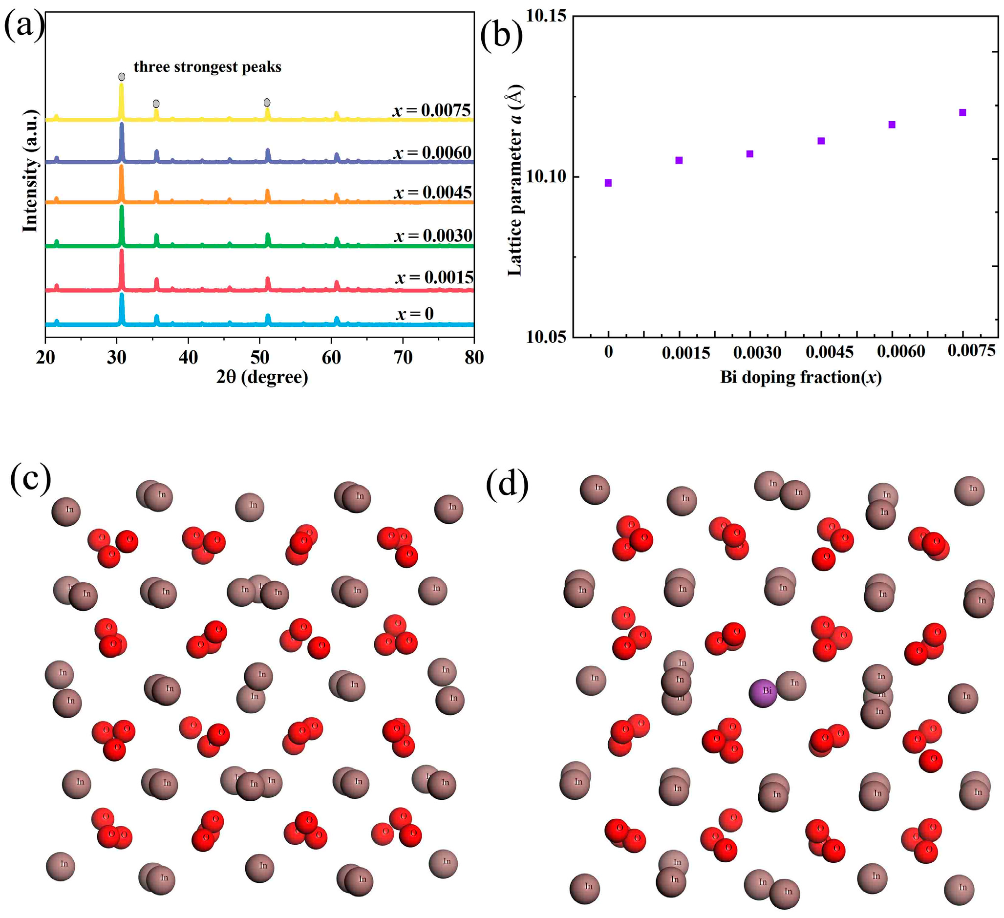
The XRD patterns of Bi-doped In
2O
3 samples, as shown in
Figure 1, show no evidence of secondary phases. This indicates that Bi atoms are successfully incorporated into the In
2O
3 lattice without forming separate compounds. In
2O
3 has a cubic bixbyite-type structure. When Bi is doped into the In
2O
3 lattice, the absence of secondary phases suggests that the doping process is well-controlled. Bi atoms likely substitute for In
3+ ions in the lattice. According to the principle of ionic substitution, for a substitution to occur without forming a secondary phase, the ionic sizes and valences of the substituting and host ions need to be compatible to some extent. The ionic radius of In
3+ (coordination number 6) is approximately 80 pm, while that of Bi
3+ (coordination number 6) is around 103 pm. Although there is a size difference between In
3+ and Bi
3+, the crystal lattice of In
2O
3 can accommodate a certain degree of lattice distortion to incorporate Bi atoms. The valences of In
3+ and Bi
3+ are the same, which also facilitates the substitution process. This substitution occurs in a way that maintains the overall crystal structure of In
2O
3, resulting in the absence of secondary phases in the XRD patterns. One of the most notable findings from the XRD analysis is the increase in the lattice constant of Bi-doped In
2O
3 samples. The increase in the lattice constant can be attributed to several factors related to the doping process. As mentioned earlier, the ionic radius of Bi
3+ is larger than that of In
3+. When Bi
3+ substitutes for In
3+ in the In
2O
3 lattice, the larger-sized Bi
3+ ions cause the lattice to expand. This expansion is a natural response of the crystal structure to accommodate the larger dopant ions. According to the Vegard’s law [
26,
27,
28], which describes the relationship between the lattice parameter of a solid solution and the composition of its components, the lattice constant of a solid solution is a linear function of the atomic fraction of the components in an ideal case. In the case of Bi-doped In
2O
3, the increase in the lattice constant is consistent with the larger ionic size of Bi
3+ compared to In
3+. In addition to the ionic size effect, charge compensation mechanisms may also play a role in the lattice expansion. Bi can exist in multiple oxidation states, such as +3 and +5. When Bi is doped into In
2O
3, charge-neutrality needs to be maintained in the lattice. If Bi is present in a +5 oxidation state, for example, it will introduce additional positive charges. To compensate for these extra charges, the lattice may undergo structural adjustments, which can contribute to the increase in the lattice constant. Furthermore, the crystal field effects can also influence the lattice structure. The different electronic configurations of In
3+ and Bi
3+ ions result in different crystal field interactions with the surrounding oxygen ions. These interactions can affect the bond lengths, as shown in
Table 1, calculated using Materials Studio, and angles in the lattice, leading to an expansion of the unit cell and an increase in the lattice constant. The Sigmas used for celref iteration is shown in
Table 2. The structural changes observed in the XRD analysis have significant implications for the thermoelectric properties of Bi-doped In
2O
3. The absence of secondary phases ensures the integrity of the host lattice, which is beneficial for maintaining the desired electrical and thermal transport properties. A pure-phase material has fewer interfaces and defects that could scatter charge carriers or phonons, which are crucial for efficient thermoelectric energy conversion. The increase in the lattice constant can have a positive impact on the thermoelectric figure of merit (ZT). The larger lattice constant can lead to a reduction in the phonon mean-free path, which in turn decreases the thermal conductivity of the material. Since thermoelectric efficiency is related to the ratio of electrical conductivity to thermal conductivity, a decrease in thermal conductivity can potentially enhance the ZT value. Additionally, the doping-induced changes in the electronic structure, which are related to the lattice-structure modifications, can also optimize the electrical conductivity, further contributing to the improvement in thermoelectric performance.
After analyzing the XRD patterns and lattice constant changes in the previous section, this section delves into the analysis of electronic transport properties, including electrical conductivity, carrier concentration, and mobility, as well as the examination of the band structure and density of states. These aspects are crucial for understanding the underlying mechanisms of how Bi-doping affects the performance of In
2O
3 based thermoelectric materials. In the case of Bi-doped In
2O
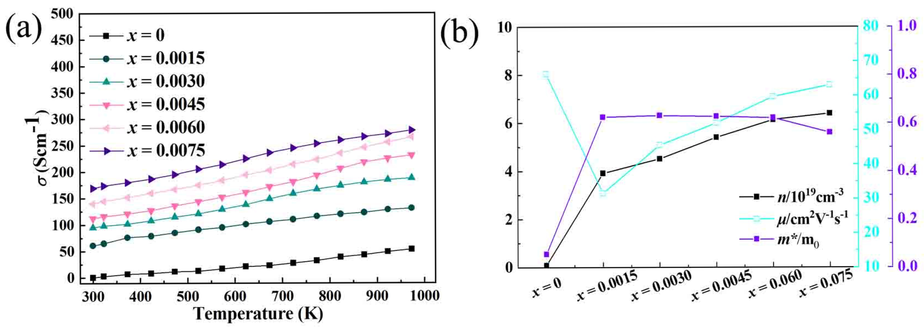
3, the experimental results show an increase in electrical conductivity, as shown in
Figure 2. The electrical conductivity for the undoped In
2O
3 is 53.420 Scm
−1, which was increased to 131.123 Scm
−1, 188.131 Scm
−1, 231.412 Scm
−1, 265.125 Scm
−1, 278.114 Scm
−1 for
x = 0.0015, 0.0030, 0.0045, 0.0060, 0.0075, respectively. This increase can be primarily attributed to the change in carrier concentration, as shown in
Figure 2. The carrier concentration of the samples is 0.086 × 10
19 cm
−1, 3.914 × 10
19 cm
−1, 4.513 × 10
19 cm
−1, 5.409 × 10
19 cm
−1, 6.139 × 10
19 cm
−1, 6.401 × 10
19 cm
−1 for
x = 0.0015, 0.0030, 0.0045, 0.0060, 0.0075, respectively. Although the mobility decreases, the overall conductivity is still improved due to the significant increase in carrier concentration. When Bi is doped into the In
2O
3 lattice, it may act as a donor. As mentioned before, Bi can exist in multiple oxidation states. In the In
2O
3 lattice, if Bi
3+ substitutes for In
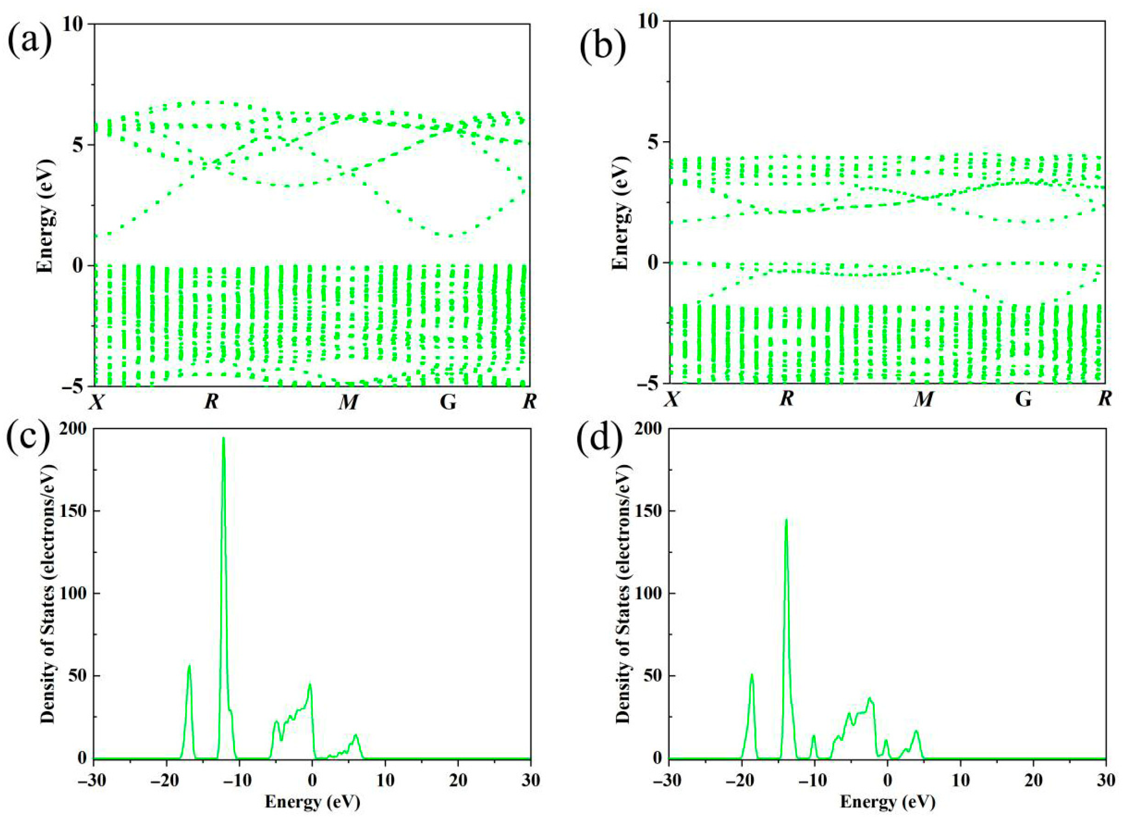
3+, there is no net change in charge contribution from the substitution itself. However, due to the unique electronic structure of Bi, as shown in
Figure 3,
Figure 4 and
Figure 5, it can introduce additional electrons into the conduction band of In
2O
3. For example, in some cases, the doping process may cause a small fraction of Bi atoms to lose more electrons than the In atoms they replace, effectively increasing the number of free electrons in the conduction band [
29,
30,
31]. In
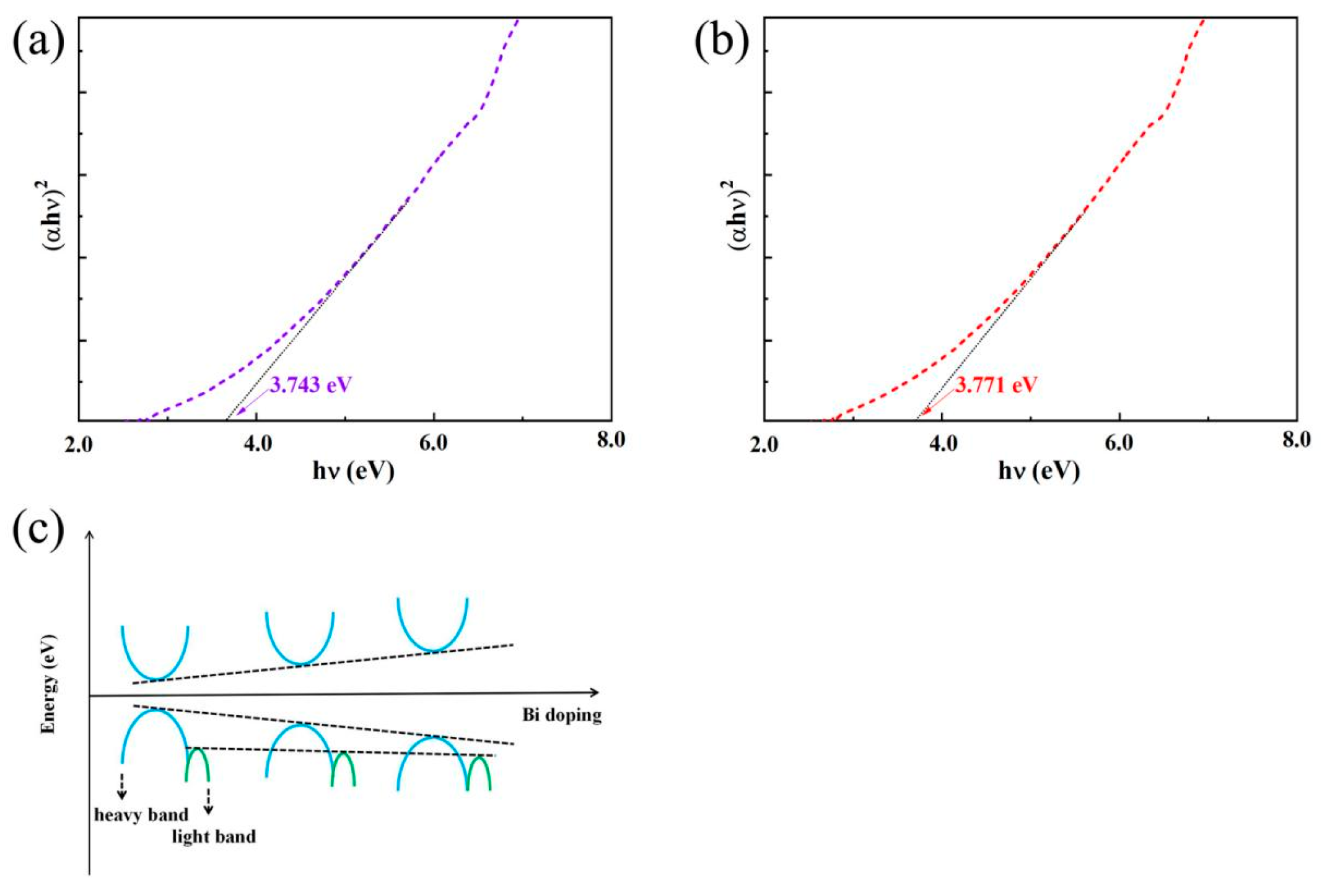
Figure 5, the optical band gap can be calculated using the following equation from reference [
32,
33]: (
αhυ)
2 = C(
hυ − E
g). Here,
α represents the absorption coefficient,
h is Planck’s constant,
υ is the photon frequency, C is a constant, and E
g denotes the band gap. To determine the band gap, one can extrapolate the linear region near the absorption onset from a plot of (
αhυ)
2 versus
hυ. According to the Beer–Lambert Law,
A = lg (1/T) =
αbc, where
A is the absorbance,
T is the transmittance,
b is the sample thickness, and
c is the concentration. When
b and
c are fixed,
α is proportional to
A. Thus,
A can be derived from
T, and the band gap can be obtained by extrapolating the linear region near the onset in a plot of (
αhυ)
2 versus
hυ. Another possible mechanism is related to the lattice distortion caused by Bi-doping. The larger ionic radius of Bi
3+ compared to In
3+ leads to lattice expansion. This lattice distortion can modify the electronic band structure of In
2O
3. According to the theory of semiconductor physics, a change in the lattice structure can affect the energy levels of electrons. In the case of Bi-doped In
2O
3, the lattice distortion may cause the conduction band to become more dispersive. A more dispersive conduction band implies that electrons have more accessible states to occupy at a specific energy level, which can in turn boost the probability of electron transport and thereby enhance electrical conductivity. The increase in carrier concentration resulting from Bi-doping is a key factor that contributes to the improved electrical conductivity. As Bi atoms are incorporated into the In
2O
3 lattice, they can introduce additional charge carriers. In the context of semiconductor doping, this is similar to n-type doping. Bi atoms can donate electrons to the conduction band of In
2O
3. The exact mechanism of carrier generation depends on the oxidation state of Bi in the lattice. If Bi is in a +5 oxidation state when substituting for In
3+, it brings two extra electrons into the system. These extra electrons are then available for conduction. The increase in carrier concentration can be further explained from the perspective of defect chemistry. Lattice distortion induced by Bi-doping may also generate certain intrinsic defects, such as oxygen vacancies. In In
2O
3, oxygen vacancies can function as electron donors. Due to the charge-compensation requirements within the lattice, the presence of Bi atoms is likely to promote the formation of oxygen vacancies. For example, if a Bi
5+ ion is incorporated, the creation of an oxygen vacancy can help maintain charge neutrality in the lattice, and at the same time, the oxygen vacancy donates two electrons to the conduction band, further increasing the carrier concentration. Despite the increase in carrier concentration and electrical conductivity, the carrier mobility in Bi-doped In
2O
3 shows a decrease. Carrier mobility is a measure of how easily charge carriers can move through the material under the influence of an electric field. The larger ionic radius of Bi
3+ compared to In
3+ causes lattice distortion. This lattice distortion creates additional scattering centers for charge carriers. As electrons move through the lattice, they interact with lattice atoms. In a perfect crystal lattice, electrons can move relatively freely. However, in Bi-doped In
2O
3, the lattice distortion caused by the presence of Bi atoms disrupts the lattice’s regular periodicity. Consequently, electrons are more prone to being scattered by these lattice irregularities. According to the theory of electron–phonon scattering, lattice vibrations (phonons) are also affected by such lattice distortion, and the interaction between electrons and phonons constitutes a key scattering mechanism. The distorted lattice in Bi-doped In
2O
3 leads to a change in the phonon spectrum, which in turn increases the electron–phonon scattering probability and reduces the carrier mobility. Bi atoms act as impurities in the In
2O
3 lattice. Impurity scattering is another significant factor contributing to the decrease in carrier mobility [
34,
35,
36]. The electronic structure of Bi is different from that of In. The presence of Bi atoms in the lattice creates local potential fluctuations. These potential fluctuations can scatter charge carriers. When an electron approaches a Bi atom in the lattice, the difference in the electrostatic potential between the Bi atom and the surrounding In atoms causes the electron to change its trajectory. The probability of impurity scattering depends on the concentration of Bi atoms in the lattice. As the Bi-doping concentration increases, the number of impurity-scattering centers also increases, leading to a more significant decrease in carrier mobility. An examination of the band structure, as shown in
Figure 3, reveals a widening of the band gap in Bi-doped In
2O
3 compared to undoped In
2O
3. The calculated band gap values are ~1.3 eV and ~1.7 eV, which are smaller than the experimental test values due to the error in the GGA method [
37]. The core reason for this lies in the approximate treatment of exchange-correlation energy. The discrepancy between the observed bandgap in experiments and theoretical calculations may also stem from the Burstein–Moss (B-M) shift induced by carrier concentration, an effect that is particularly pronounced in highly doped semiconductors. Bi, as a doping atom, enhances the donor effect, leading to a significant increase in carrier concentration in the material. The high concentration of free electrons fills the energy levels near the bottom of the conduction band, causing the calculated bandgap value to shrink [
38,
39,
40]. Since bismuth is a heavy atom with a strong spin–orbit coupling effect, we considered spin–orbit coupling when performing first-principles calculations. The band gap is a critical parameter in semiconductor materials, as it dictates the energy required for electrons to transition from the valence band to the conduction band. One primary reason for band-gap widening is the alteration in electronic structure induced by Bi-doping. Bi has a different electronic configuration from In; when Bi atoms are incorporated into the In
2O
3 lattice, the hybridization among the orbitals of Bi, In, and O atoms changes. The outermost electrons of Bi exhibit different energy levels and spatial distributions compared to those of In, and this change in orbital hybridization causes a shift in the energy levels of both the valence band and the conduction band. In particular, the conduction band minimum (CBM) energy may shift upward, and the valence band maximum (VBM) energy may shift downward, resulting in an overall widening of the band gap. Another factor contributing to the band-gap widening is the lattice distortion. As mentioned earlier, the larger ionic radius of Bi
3+ causes lattice expansion. The change in the lattice parameters affects the crystal-field potential experienced by the electrons in the lattice. This change in the crystal-field potential can modify the energy levels of the valence and conduction bands, leading to a wider band gap. The density of states (DOS) near the Fermi level shows a slight increase in Bi-doped In
2O
3, as depicted in
Figure 3 and
Figure 4 (partial density of states). The density of states represents the number of available electronic states per unit energy interval. The increase in the density of states near the Fermi level can be related to the introduction of new energy levels by Bi-doping [
41,
42,
43]. Bi atoms have their own set of electronic energy levels. When they are incorporated into the In
2O
3 lattice, these energy levels interact with the energy levels of In
2O
3. Some of the energy levels of Bi may fall close to the Fermi level of In
2O
3, increasing the number of available states in this energy region. In addition, the lattice distortion and the resulting change in the electronic band structure can also contribute to an increase in the density of states near the Fermi level. The lattice distortion can cause the energy bands to become more complex, with the formation of sub-bands and local states. These additional states near the Fermi level increase the density of states in this region. Yan et al. reported that Bi-doping induces deep gap states in In
2O
3 [
44], leading to enhanced sub-bandgap absorption, which seems contradictory to the band gap widening observed in our study. We propose that this discrepancy may arise from the significant difference in doping concentrations. In the heavily doped samples of our study, high carrier concentration fills the bottom of the conduction band, causing the Fermi level to enter the conduction band and resulting in a Burstein–Moss shift [
45,
46,
47]. This shifts the optical absorption edge to higher energies, forming an apparent band gap widening. This phenomenon is not an intrinsic broadening of the band gap but a result of carrier concentration regulation, which does not conflict with the deep level state induction effect under low doping conditions reported by Yan et al. The increase in electrical conductivity due to the increase in carrier concentration, despite the decrease in mobility, can have a positive impact on the thermoelectric figure of merit (ZT). Although the decrease in mobility may seem disadvantageous, the significant increase in carrier concentration can still lead to an overall increase in electrical conductivity. This increase in electrical conductivity can enhance the numerator of the ZT formula, potentially improving the thermoelectric performance.
In the study of Bi-doped indium oxide (In
2O
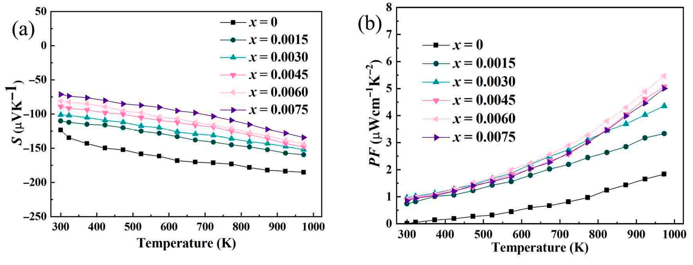
3) thermoelectric materials, the observed decrease in the absolute value of the Seebeck coefficient after Bi-doping, as shown in
Figure 6a, is an interesting phenomenon that warrants in-depth analysis. Bi-doping leads to an increase in the carrier concentration in In
2O
3. In general, for a degenerate semiconductor like Bi-doped In
2O
3 (where the carrier concentration is relatively high), the Seebeck coefficient has an inverse relationship with the carrier concentration [
48,
49,
50]. According to the Mott formula for the Seebeck coefficient in a degenerate semiconductor. When the carrier concentration increases, the number of charge carriers available for conduction at the Fermi level increases. The widening of the band gap as shown in
Figure 3,
Figure 4 and
Figure 5 in Bi-doped In
2O
3 plays a role in the change in the Seebeck coefficient. With a wider band gap, the number of thermally excited electrons that can cross the band gap from the valence band to the conduction band is reduced. A wider band gap means that the energy range for efficient charge-carrier transport across the temperature gradient is limited. The electrons in the conduction band are mainly responsible for the thermoelectric transport. When the band gap widens, the density of available states in the conduction band near the band-gap edge changes. This change in the density of states affects the energy-dependent distribution of charge carriers. As a result, the Seebeck coefficient, which is sensitive to the energy-dependent transport of charge carriers, decreases in absolute value.
In the study of Bi-doped indium oxide (In
2O
3) thermoelectric materials, the observed increase in the power factor after Bi-doping, as shown in
Figure 6b, despite the decrease in the absolute value of the Seebeck coefficient, is a phenomenon that requires in-depth analysis. As noted earlier, Bi-doping brings about a significant increase in the carrier concentration of In
2O
3 and a rise in electrical conductivity that can contribute to an elevated power factor, even as the absolute value of the Seebeck coefficient decreases. However, the power factor is proportional to the square of the Seebeck coefficient. The increase in electrical conductivity can still result in an overall increase in the power factor. The decrease in carrier mobility in Bi-doped In
2O
3 is mainly caused by lattice scattering and impurity scattering. The larger ionic radius of Bi
3+ compared to In
3+ leads to lattice distortion, creating additional scattering centers for charge carriers. Bi atoms themselves also act as impurities, causing impurity scattering. The widening of the band gap in Bi-doped In
2O
3 primarily influences the power factor through its effect on the Seebeck coefficient. A broader band gap reduces the number of thermally excited electrons that cross from the valence band to the conduction band. This restricts the energy range for efficient charge-carrier transport across the temperature gradient, resulting in a decrease in the Seebeck coefficient. Nevertheless, in some instances, band-gap widening can also alter the electronic band structure, which may reduce charge-carrier scattering at specific energy levels—an effect that could have a positive but minor impact on electrical conductivity. The slight increase in the density of states near the Fermi level in Bi-doped In
2O
3 has a dual effect. On one hand, it makes the energy-dependent distribution of charge carriers more uniform, reducing the Seebeck coefficient. On the other hand, it increases the number of available charge carriers for conduction, contributing to the increase in electrical conductivity. In the case of Bi-doped In
2O
3, the positive effect on electrical conductivity outweighs the negative impact on the Seebeck coefficient, resulting in an increase in the power factor.
In Bi-doped In
2O
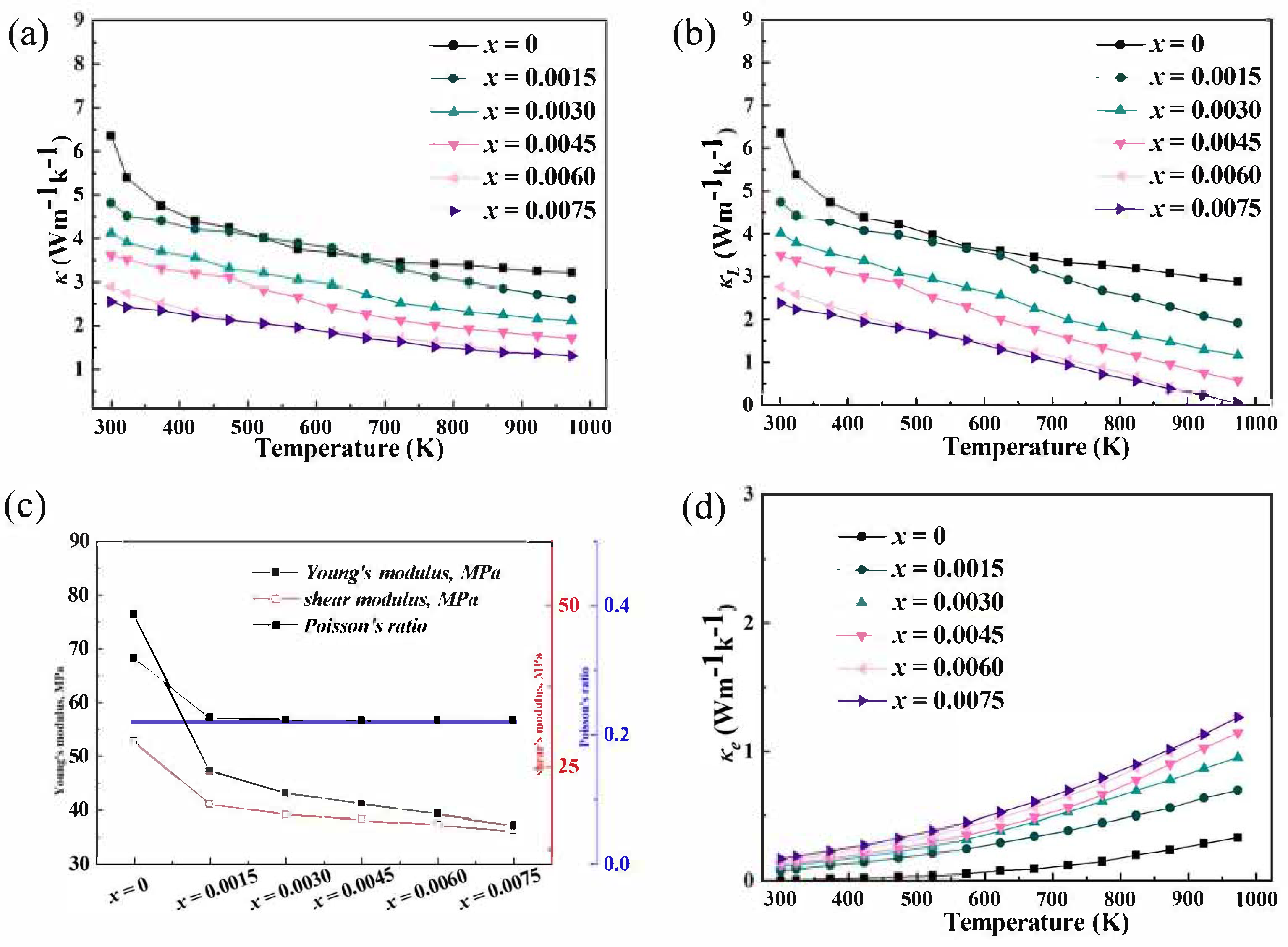
3, the observed decrease in thermal conductivity, as shown in
Figure 7a, can be primarily attributed to the increase in lattice scattering. The thermal conductivity of indium oxide is ~6.35 Wm
−1K
−1 at room temperature and ~3.22 Wm
−1K
−1 at 973 K. After Bi-doping, the lowest thermal conductivity reaches ~2.55 Wm
−1K
−1 at room temperature and ~1.31 Wm
−1K
−1 at 973 K. The larger ionic radius of Bi
3+ compared to In
3+ causes significant lattice distortion. This lattice distortion creates additional scattering centers for phonons, which are carriers of lattice heat [
51,
52,
53]. According to the kinetic theory of heat conduction, with the decrease in the mean-free path of phonons due to lattice scattering, the lattice thermal conductivity decreases. The decrease in the absolute value of the Seebeck coefficient is related to the increase in carrier concentration, which makes the energy-dependent distribution of charge carriers more uniform. This change in the charge-carrier distribution also affects the thermal conductivity. A more uniform distribution of charge carriers reduces the energy-filtering effect, which in turn reduces the contribution of the Seebeck-related thermoelectric effect to the thermal conductivity. The widening of the band gap in Bi-doped In
2O
3 not only affects the electronic and thermal transport properties but also the lattice dynamics. The change in the energy levels of the valence and conduction bands due to band-gap widening can modify the phonon–electron interaction. This modification can lead to an increase in phonon scattering, further reducing the lattice thermal conductivity. The slight increase in the density of states near the Fermi level has a complex effect on the thermal conductivity. On one hand, it can increase the number of available charge carriers for conduction, which might contribute to the electronic thermal conductivity. On the other hand, it also makes the energy-dependent distribution of charge carriers more uniform, reducing the Seebeck-related contribution to the thermal conductivity. As shown in
Figure 7b, the Young’s modulus of Bi-doped In
2O
3 is reduced. The specific numerical value is ~76.49 MPa, ~47.23 MPa, ~43.12 MPa, ~41.21 MPa, ~39.32 MPa, and ~37.13 MPa for
x = 0, 0.015, 0.030, 0.045, 0.060, and 0.075, respectively. The main reason for this reduction is the lattice distortion caused by Bi-doping. The larger Bi
3+ ions introduce internal stress in the lattice, weakening the inter-atomic bonds. A lower Young’s modulus indicates a softer material, which means that the lattice is more easily deformed. This softening of the lattice has a direct impact on the thermal conductivity. A softer lattice leads to more phonon-phonon scattering. The reduced stiffness of the lattice allows for more complex lattice vibrations, which increases the probability of phonon–phonon scattering events.
In the research on Bi-doped indium oxide (In
2O
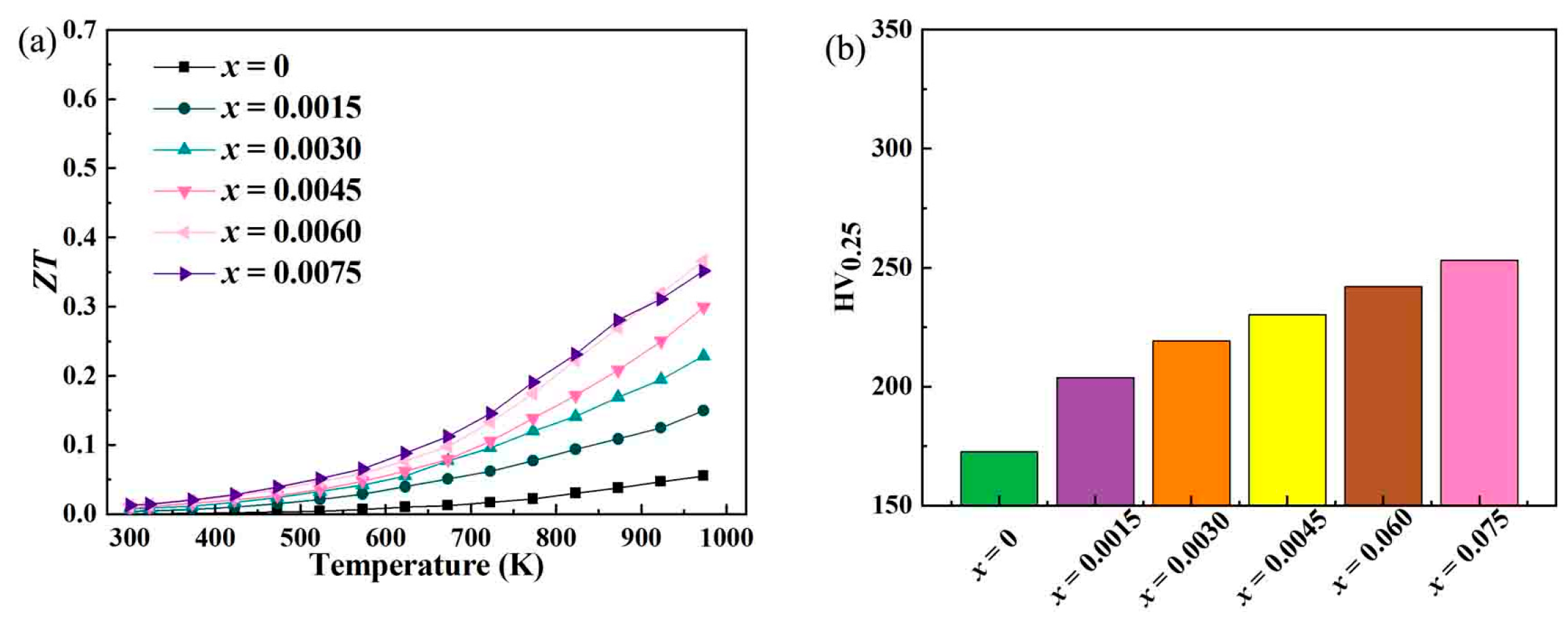
3) thermoelectric materials, comprehending the factors underlying the substantial increase in ZT, as depicted in
Figure 8, is of the utmost importance for evaluating their potential in practical thermoelectric applications. The highest ZT value has increased from 0.055 for the undoped In
2O
3 to 0.0124 for
x = 0.0015, 0.200 for
x = 0.0030, 0.288 for
x = 0.0045, 0.402 for
x = 0.0060, and 0.372 for
x = 0.0075 at 973 K. In this study, the maximum ZT value obtained for Bi-doped indium oxide is approximately 0.402, higher than the 0.18 obtained for Ge doping [
54] and 0.09 for Mo doping [
20], but lower than the 0.42 obtained for V doping [
21]. This result indicates that, compared with Ge or Mo, Bi has a greater advantage in balancing the regulation of carrier concentration and mobility. As is evident from the experimental data, Bi-doping leads to a notable decrease in the thermal conductivity of In
2O
3. The lattice distortion induced by the larger ionic radius of Bi
3+ compared to In
3+ gives rise to an abundance of additional scattering centers for phonons. These scattering centers impede the free movement of phonons, thereby reducing the lattice thermal conductivity. For instance, the distorted lattice structure disrupts the regular propagation of lattice vibrations, causing phonons to collide more frequently and shortening their mean-free path. Simultaneously, the modification of the electronic structure, such as the widening of the band gap, plays a role in reducing the electronic thermal conductivity. With a wider band gap, fewer electrons are thermally excited and available for heat conduction. Since ZT is inversely proportional to thermal conductivity, a decrease in thermal conductivity has a direct and positive impact on ZT. A lower thermal conductivity implies that less heat is wasted during the thermoelectric conversion process, allowing for a more efficient transformation of thermal energy into electrical energy. For example, if the thermal conductivity is reduced by a factor of three while other parameters remain constant, the ZT value will triple, assuming the power factor remains unchanged. The power factor experiences a remarkable increase after Bi-doping. The increase in carrier concentration, despite the concurrent decrease in carrier mobility, exerts a dominant influence on the electrical conductivity. Bi-doping introduces additional electrons into the In
2O
3 lattice, which act as charge carriers and enhance the electrical conduction. Although the absolute value of the Seebeck coefficient decreases, the upsurge in electrical conductivity is substantial enough to result in an overall increase in the power factor. Given that ZT is directly proportional to the power factor, an enhanced power factor is a major contributor to the significant increase in ZT. A higher power factor means that the material can generate more electrical power per unit cross-sectional area and temperature gradient. For instance, if the power factor doubles and the thermal conductivity remains constant, the ZT value will also double, highlighting the crucial role of the power factor in determining the thermoelectric performance. The decrease in the absolute value of the Seebeck coefficient is closely related to the increase in carrier concentration. A higher carrier concentration makes the energy-dependent distribution of charge carriers more uniform, diminishing the energy-filtering effect that is essential for a high Seebeck coefficient. However, in the context of the power factor, the decrease in Seebeck coefficient, is compensated by the significant increase in electrical conductivity. The increase in carrier concentration and the decrease in carrier mobility have intricate effects on ZT. The augmented carrier concentration boosts the electrical conductivity, which is beneficial for the power factor. Nevertheless, the decrease in mobility, caused by lattice and impurity scattering, has the potential to limit the further enhancement of the power factor. In the case of Bi-doped In
2O
3, the positive effect of the increased carrier concentration on the power factor prevails over the negative impact of the decreased mobility, contributing to the overall increase in ZT. The widening of the band gap in Bi-doped In
2O
3 has multiple implications for ZT. It reduces the number of thermally excited electrons, which in turn decreases the electronic thermal conductivity, positively affecting ZT. However, it also curtails the Seebeck coefficient by restricting the energy-filtering effect. The overall impact on ZT hinges on the combined effect of these changes on the power factor and thermal conductivity. The slight increase in the density of states near the Fermi level modifies the energy-dependent transport of charge carriers. It augments the number of available charge carriers for conduction, contributing to the increase in the power factor. Simultaneously, it makes the energy-dependent distribution of charge carriers more uniform, reducing the Seebeck-related contribution to the thermal conductivity. The combined effect of these changes on the power factor and thermal conductivity ultimately determines the significant increase in ZT. The substantial increase in the thermoelectric figure of merit in Bi-doped In
2O
3 thermoelectric materials is the outcome of the combined influence of a decrease in thermal conductivity, an increase in the power factor, alterations in the Seebeck coefficient, carrier-related properties, band-gap widening, and a slight increase in the density of states near the Fermi level. The reduction in thermal conductivity and the enhancement of the power factor play the most prominent roles in elevating ZT. The electronic structure of Bi atoms is different from that of the indium oxide matrix. During doping, electrons are transferred from Bi to In sites, resulting in a change in the In active sites, thus regulating the local charge structure of the indium oxide material and affecting its electrical properties. There is a difference in the radius between Bi atoms and In atoms. Lattice distortion will be caused after doping. This may produce lattice strain and form defects such as dislocations. An appropriate amount of lattice distortion and defects can change the scattering mechanism of carriers, and also have an impact on phonon scattering, thereby affecting the thermoelectric properties of the material. Bi-doping can increase the carrier concentration in indium oxide. More carriers are helpful to improve the electrical conductivity. At the same time, by reasonably regulating the doping amount and energy-band structure, the Seebeck coefficient can also be optimized. The synergistic effect of the two can increase the power factor, thus increasing the ZT value. To further optimize the ZT value of Bi-doped In
2O
3, future research should concentrate on precisely adjusting the Bi-doping concentration to strike a balance among the various property changes—for example, identifying the optimal doping concentration that maximizes the power factor while minimizing the adverse effects on the Seebeck coefficient and carrier mobility. Additionally, exploring novel strategies to further reduce the thermal conductivity, such as nanostructuring or the utilization of composite materials, holds the promise of significantly enhancing the overall thermoelectric performance of Bi-doped In
2O
3. A profound understanding of these complex relationships is indispensable for the development of high-performance Bi-doped In
2O
3 thermoelectric materials for practical applications in energy-harvesting and waste-heat recovery.
As shown in
Figure 8b, the Vickers hardness of Bi-doped In
2O
3 increased. One of the primary reasons for this is the lattice distortion caused by Bi-doping. The larger ionic radius of Bi
3+ compared to In
3+ disrupts the regular lattice structure of In
2O
3. This distortion leads to an increase in the resistance to plastic deformation. When an external force is applied during the Vickers hardness test, the distorted lattice structure makes it more difficult for the atoms to slide past each other. Moreover, the introduction of Bi atoms can change the inter-atomic bonding in the In
2O
3 lattice. Bi atoms may form stronger chemical bonds with the surrounding oxygen atoms compared to In atoms. This increase in the strength of the inter-atomic bonds enhances the overall resistance of the material to indentation during the Vickers hardness measurement. Another factor is the pinning effect on dislocations. The presence of Bi atoms can act as obstacles to the movement of dislocations. Dislocations are defects in the crystal lattice that are responsible for plastic deformation. By impeding the movement of dislocations, Bi-doping effectively increases the hardness of the material. When a load is applied in the Vickers hardness test, the dislocations are less likely to move and cause plastic deformation, resulting in a higher measured Vickers hardness value.
