
Mechanical Modelling of Integration and Debonding Process of Ultra-Thin Inorganic Chips


Abstract
1. Introduction
2. Results
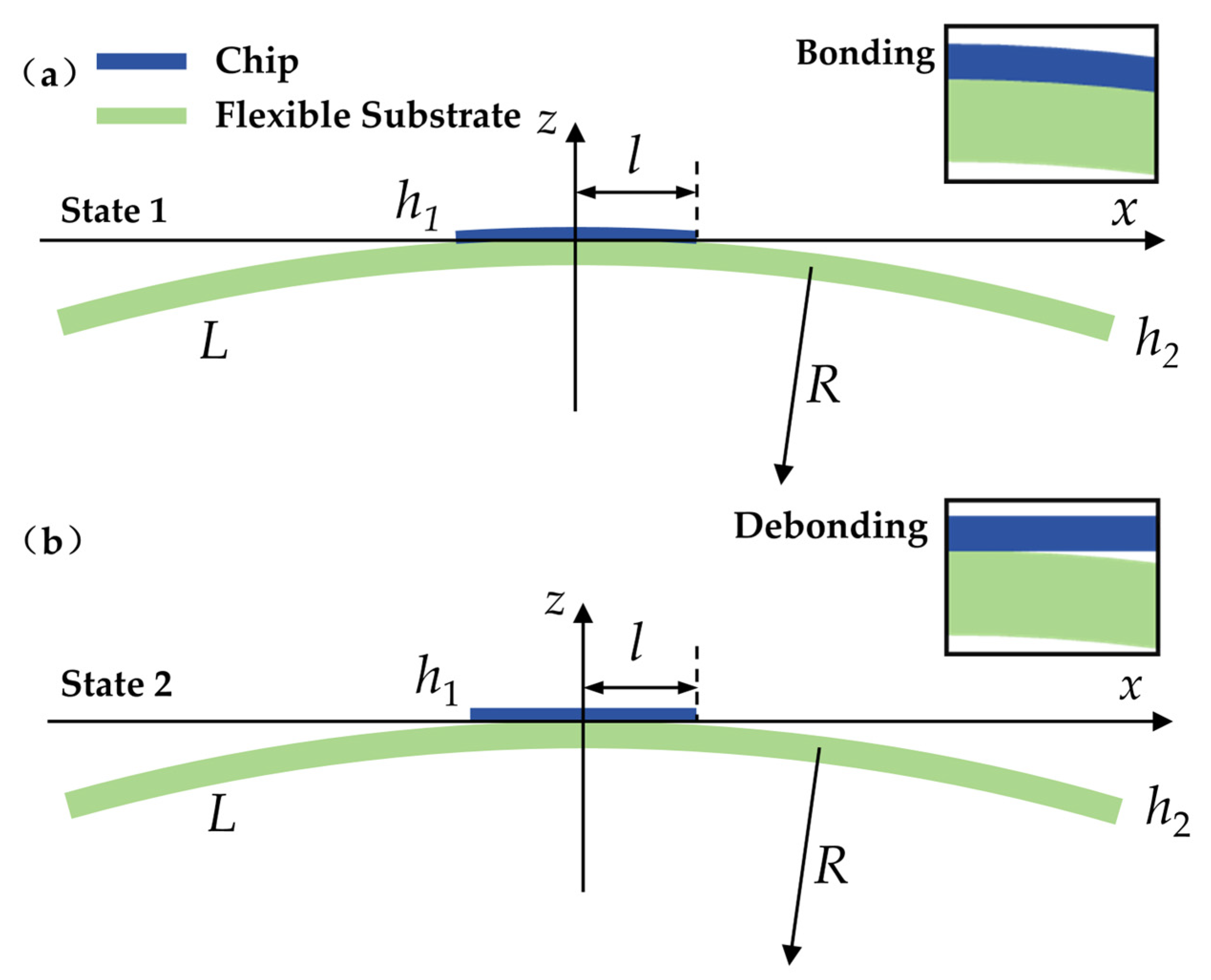
2.1. Modeling
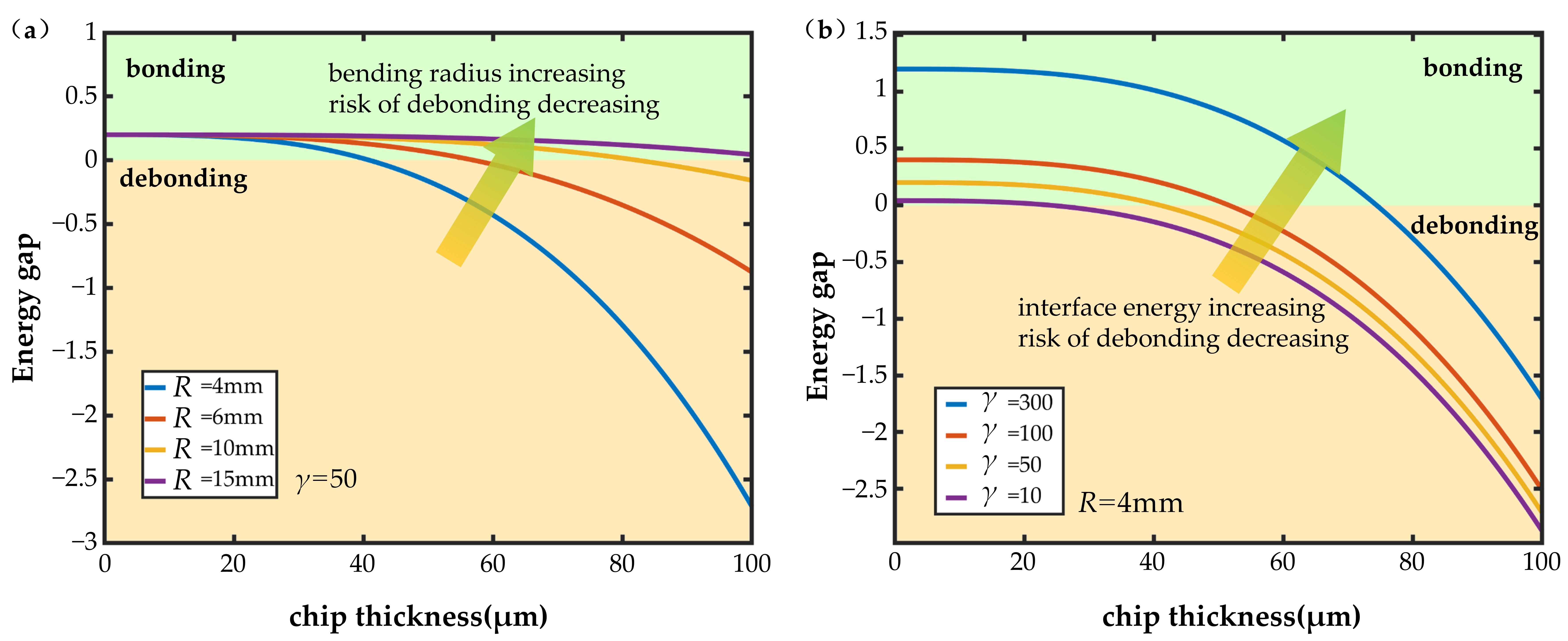
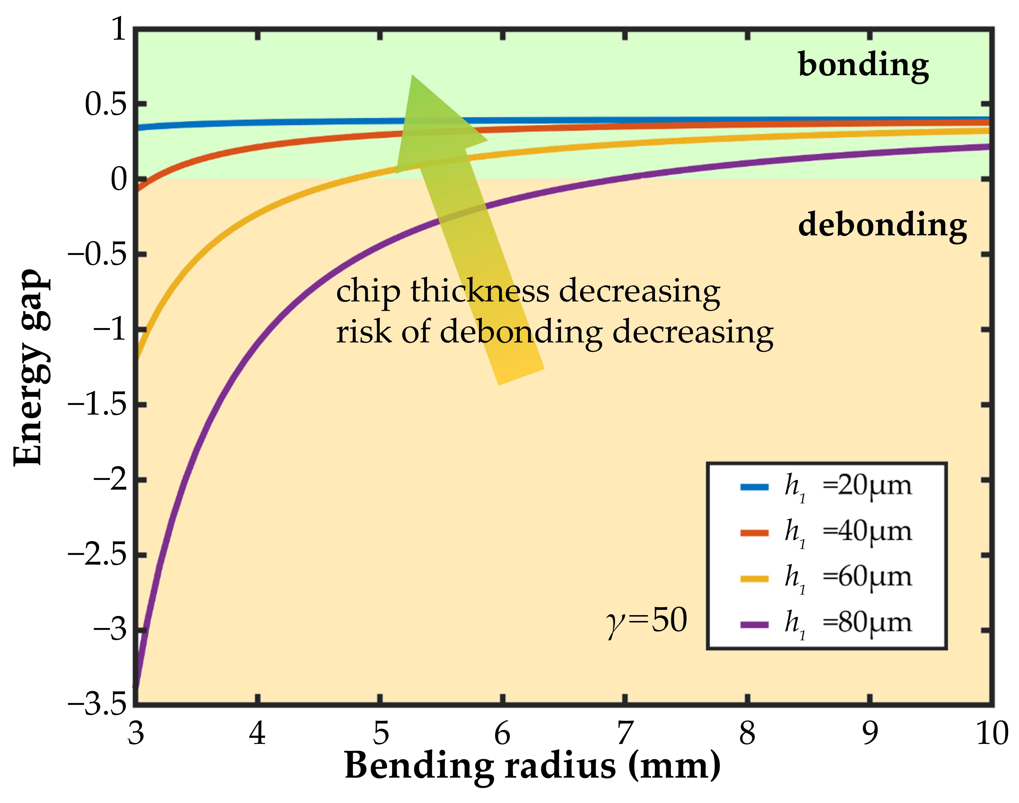
2.2. Effect of Various Parameters
3. Discussion
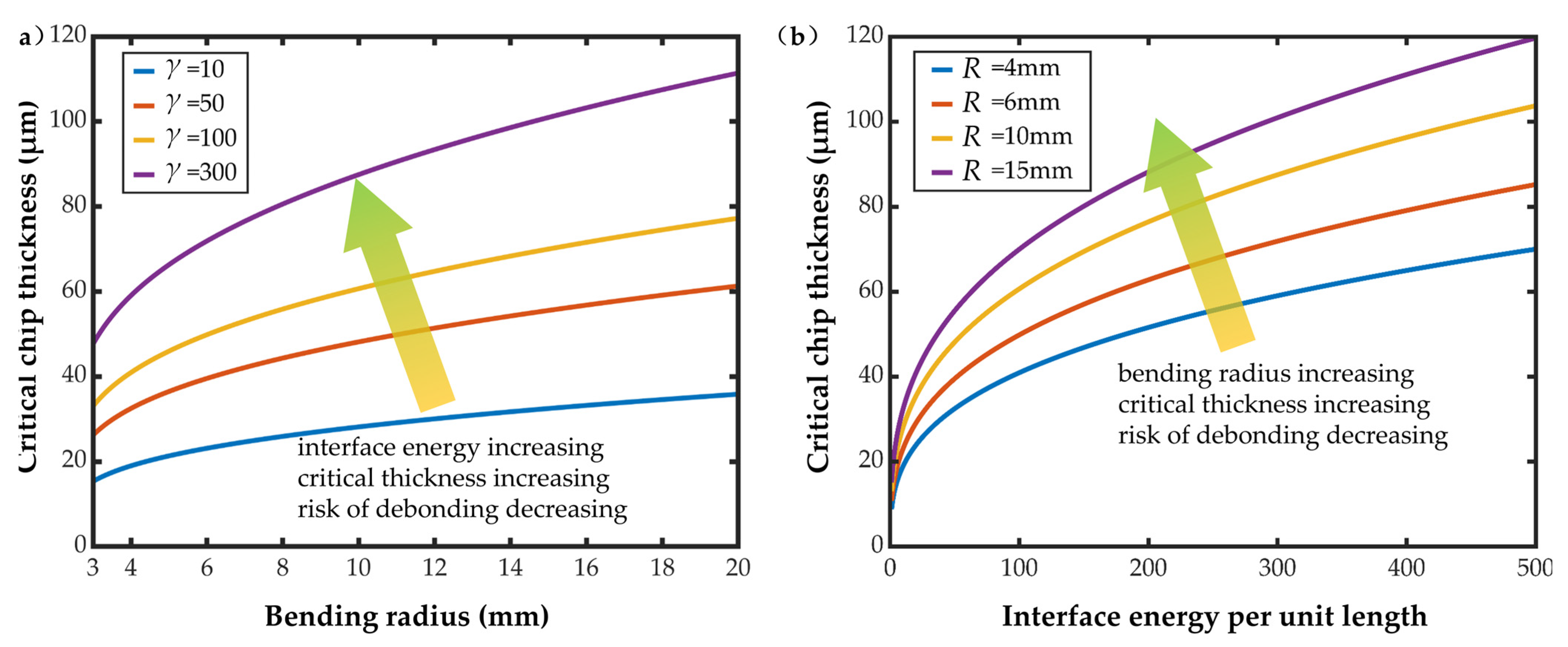
3.1. Critical Thickness
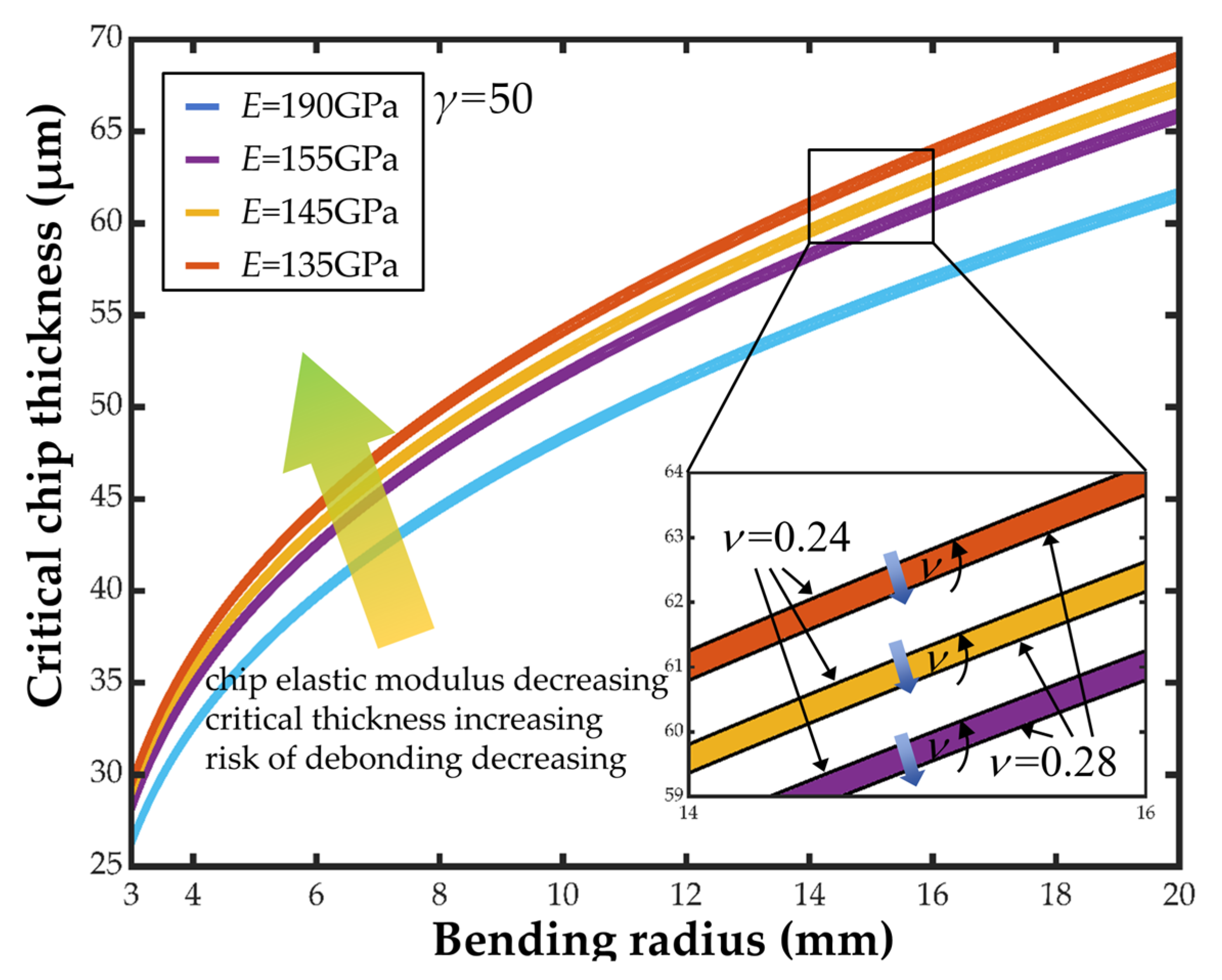
3.2. Effect of Changes in Silicon Material Properties
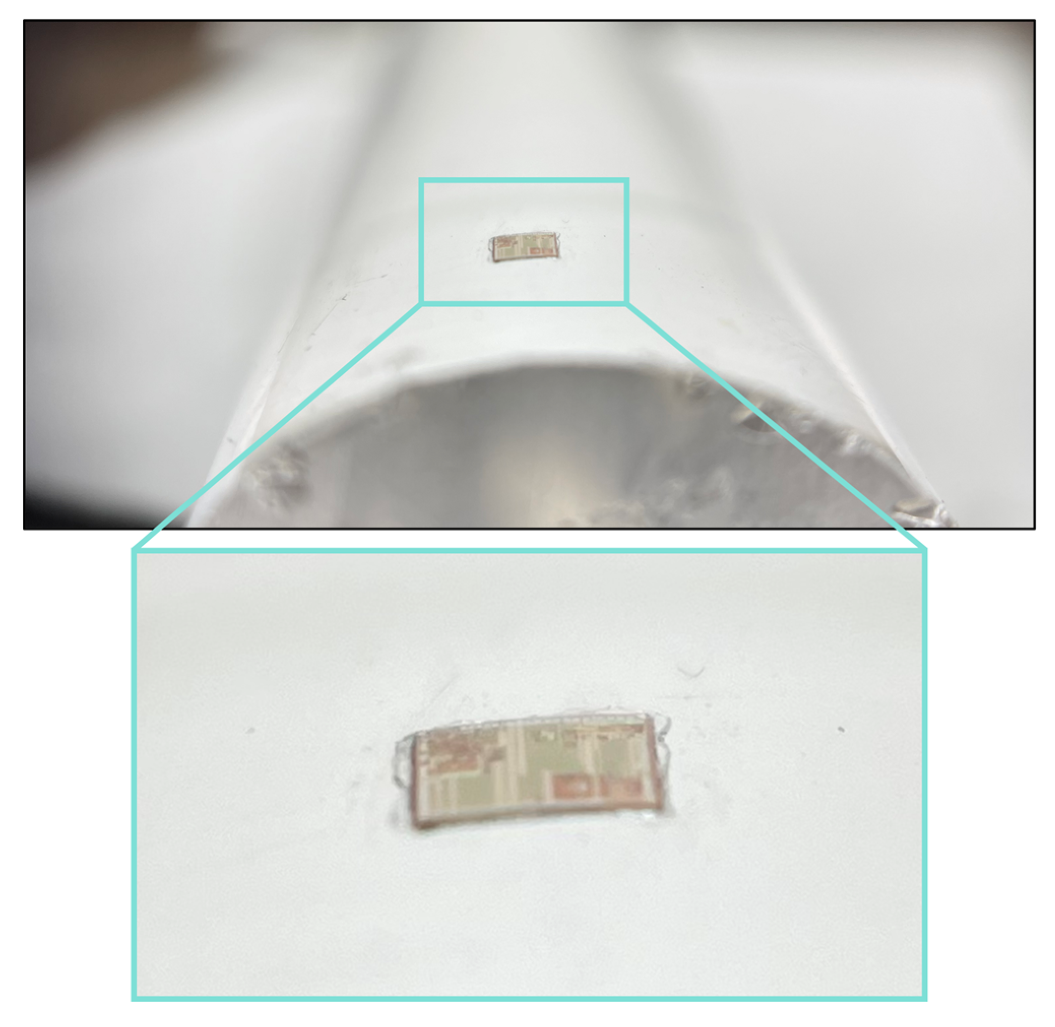
3.3. Chip Bending Experiment
3.4. Interfacial Adhesion-Regulating Layer
4. Materials and Methods
5. Conclusions
Author Contributions
Funding
Institutional Review Board Statement
Informed Consent Statement
Data Availability Statement
Conflicts of Interest
References
- Sun, Y.; Choi, W.M.; Jiang, H.; Huang, Y.Y.; Rogers, J.A. Controlled buckling of semiconductor nanoribbons for stretchable electronics. Nat. Nanotechnol. 2006, 1, 201–207. [Google Scholar] [PubMed]
- Mack, S.; Meitl, M.; Baca, A.; Zhu, Z.-T.; Rogers, J. Mechanically flexible thin-film transistors that use ultrathin ribbons of silicon derived from bulk wafers. Appl. Phys. Lett. 2006, 88, 213101. [Google Scholar]
- Im, J.-H.; Luo, J.; Franckevicius, M.; Pellet, N.; Gao, P.; Moehl, T.; Zakeeruddin, S.M.; Nazeeruddin, M.K.; Grätzel, M.; Park, N.-G. Nanowire perovskite solar cell. Nano Lett. 2015, 15, 2120–2126. [Google Scholar] [PubMed]
- Chen, Y.; Lu, B.; Chen, Y.; Feng, X. Breathable and stretchable temperature sensors inspired by skin. Sci. Rep. 2015, 5, 11505. [Google Scholar]
- Kim, J.-J.; Han, M.-K.; Noh, Y.-Y. Flexible OLEDs and organic electronics. Semicond. Sci. Technol. 2011, 26, 030301. [Google Scholar]
- Huang, Z.; Hao, Y.; Li, Y.; Hu, H.; Wang, C.; Nomoto, A.; Pan, T.; Gu, Y.; Chen, Y.; Zhang, T. Three-dimensional integrated stretchable electronics. Nat. Electron. 2018, 1, 473–480. [Google Scholar]
- Chen, Y.; Lu, S.; Zhang, S.; Li, Y.; Qu, Z.; Chen, Y.; Lu, B.; Wang, X.; Feng, X. Skin-like biosensor system via electrochemical channels for noninvasive blood glucose monitoring. Sci. Adv. 2017, 3, e1701629. [Google Scholar]
- Yoon, J.; Baca, A.J.; Park, S.-I.; Elvikis, P.; Geddes III, J.B.; Li, L.; Kim, R.H.; Xiao, J.; Wang, S.; Kim, T.-H. Ultrathin silicon solar microcells for semitransparent, mechanically flexible and microconcentrator module designs. Nat. Mater. 2008, 7, 907–915. [Google Scholar]
- Wang, F.; Wu, D.; Jin, P.; Zhang, Y.; Yang, Y.; Ma, Y.; Yang, A.; Fu, J.; Feng, X. A flexible skin-mounted wireless acoustic device for bowel sounds monitoring and evaluation. Sci. China Inf. Sci. 2019, 62, 202402. [Google Scholar]
- Klauk, H.; Halik, M.; Zschieschang, U.; Eder, F.; Rohde, D.; Schmid, G.; Dehm, C. Flexible organic complementary circuits. IEEE Trans. Electron Devices 2005, 52, 618–622. [Google Scholar]
- Kim, D.-H.; Lu, N.; Ghaffari, R.; Rogers, J.A. Inorganic semiconductor nanomaterials for flexible and stretchable bio-integrated electronics. NPG Asia Mater. 2012, 4, e15. [Google Scholar]
- Vilouras, A.; Heidari, H.; Gupta, S.; Dahiya, R. Modeling of CMOS devices and circuits on flexible ultrathin chips. IEEE Trans. Electron Devices 2017, 64, 2038–2046. [Google Scholar]
- Janek, F.; Saller, E.; Müller, E.; Meißner, T.; Weser, S.; Barth, M.; Eberhardt, W.; Zimmermann, A. Feasibility study of an automated assembly process for ultrathin chips. Micromachines 2020, 11, 654. [Google Scholar] [CrossRef] [PubMed]
- Deng, Y.-H.; Kheradmand, E.; Pang, C.; Siddik, A.B.; Bai, J.; Lieberman, I.; Geiregat, P.; Van Thourhout, D.; Hens, Z. Super Bending-Stable Flexible Colloidal QD Photodetector with Fast Response and Near-Unity Carrier Extraction Efficiency. ACS Appl. Mater. Interfaces 2025, 17, 14243–14249. [Google Scholar]
- Sharma, D.; Saroha, J.; Diksha; Vashishtha, P.; Sharma, S.N.; Ahnood, A.; Srivastava, S.K. Enhanced Performance of Flexible Hybrid Solar Cells via Silver Nanoparticle Incorporation. ACS Appl. Nano Mater. 2024, 7, 23927–23937. [Google Scholar]
- Sharma, D.; Sharma, R.K.; Srivastava, A.; Komarala, V.K.; Ahnood, A.; Prathap, P.; Srivastava, S.K. Silicon nanowire-incorporated efficient and flexible PEDOT: PSS/silicon hybrid solar cells. Sustain. Energy Fuels 2024, 8, 2969–2980. [Google Scholar]
- Gu, Y.; Li, J.; Zheng, C.; Huang, J.; Chen, Z.D.; Zhang, T.; Li, S. A flexible pressure/bending bimodal sensor for hand movements monitoring. IEEE Sens. J. 2023, 23, 30241–30248. [Google Scholar]
- Yuan, Y.; Xu, H.; Zheng, W.; Liu, M.; Li, S.; Yan, J.; Wang, D.; Liu, K.; Zhang, H.; Chen, G. Bending and Stretching-Insensitive, Crosstalk-Free, Flexible Pressure Sensor Arrays for Human-Machine Interactions. Adv. Mater. Technol. 2024, 9, 2301615. [Google Scholar]
- Peng, B.; Huang, Y.; Yin, Z.; Xiong, Y. Competing fracture modeling of thin chip pick-up process. IEEE Trans. Compon. Packag. Manuf. Technol. 2012, 2, 1217–1225. [Google Scholar]
- Liu, H.; Liu, Z.; Xu, Z.; Yin, Z.; Huang, Y.; Chen, J. Competing fracture of thin-chip transferring from/onto prestrained compliant substrate. J. Appl. Mech. 2015, 82, 101012. [Google Scholar]
- Stein, N.; Weißgraeber, P.; Becker, W. Stress solution for functionally graded adhesive joints. Int. J. Solids Struct. 2016, 97, 300–311. [Google Scholar]
- Jian, W.; Yin, H.; Chen, Y.; Feng, X. Competing behavior of interface delamination and wafer cracking during peeling film from ultra-thin wafer. Int. J. Solids Struct. 2024, 305, 113058. [Google Scholar]
- Peng, B.; Huang, Y.; Yin, Z.; Xiong, Y. Analysis of interfacial peeling in IC chip pick-up process. J. Appl. Phys. 2011, 110, 073508. [Google Scholar]
- Saiki, N.; Inaba, K.; Kishimoto, K.; Seno, H.; Ebe, K. Study on peeling behavior in pick-up process of IC chip with adhesive tapes. J. Solid Mech. Mater. Eng. 2010, 4, 1051–1060. [Google Scholar]
- Fan, X.-J.; Wang, H.; Lim, T. Investigation of the underfill delamination and cracking in flip-chip modules under temperature cyclic loading. IEEE Trans. Compon. Packag. Technol. 2002, 24, 84–91. [Google Scholar]
- Krenk, S. Energy release rate of symmetric adhesive joints. Eng. Fract. Mech. 1992, 43, 549–559. [Google Scholar]
- Park, J.E.; Jasiuk, I.; Zubelewicz, A. Stresses and fracture at the chip/underfill interface in flip-chip assemblies. J. Electron. Packag. 2003, 125, 44–52. [Google Scholar]
- Feron, M.; Zhang, Z.; Suo, Z. Split singularities and dislocation injection in strained silicon. J. Appl. Phys. 2007, 102, 023502. [Google Scholar]
- Long, H.; Liu, Y.; Wei, Y. Debonding characterization of stiff film/compliant substrate systems based on the bilinear cohesive zone model. Eng. Fract. Mech. 2022, 265, 108363. [Google Scholar]
- Fukuda, K.; Sun, L.; Du, B.; Takakuwa, M.; Wang, J.; Someya, T.; Marsal, L.F.; Zhou, Y.; Chen, Y.; Chen, H. A bending test protocol for characterizing the mechanical performance of flexible photovoltaics. Nat. Energy 2024, 9, 1335–1343. [Google Scholar]
- Zhao, J.-H.; Ryan, T.; Ho, P.S.; McKerrow, A.J.; Shih, W.-Y. Measurement of elastic modulus, Poisson ratio, and coefficient of thermal expansion of on-wafer submicron films. J. Appl. Phys. 1999, 85, 6421–6424. [Google Scholar]
- Kamiyama, E.; Sueoka, K. Method for estimating elastic modulus of doped semiconductors by using ab initio calculations—Doping effect on Young’s modulus of silicon crystal. AIP Adv. 2023, 13, 085224. [Google Scholar]
- Hopcroft, M.A.; Nix, W.D.; Kenny, T.W. What is the Young’s Modulus of Silicon? J. Microelectromech. Syst. 2010, 19, 229–238. [Google Scholar]
- Cheng, D.; Gao, Y. A critical review on the fracture of ultra-thin photovoltaics silicon wafers. Sol. Energy Mater. Sol. Cells 2024, 274, 112999. [Google Scholar]
- Yang, C.; Wu, H.; Melkote, S.; Danyluk, S. Comparative analysis of fracture strength of slurry and diamond wire sawn multicrystalline silicon solar wafers. Adv. Eng. Mater. 2013, 15, 358–365. [Google Scholar]

| 190 GPa | 0.28 | 4 mm |
Disclaimer/Publisher’s Note: The statements, opinions and data contained in all publications are solely those of the individual author(s) and contributor(s) and not of MDPI and/or the editor(s). MDPI and/or the editor(s) disclaim responsibility for any injury to people or property resulting from any ideas, methods, instructions or products referred to in the content. |
© 2025 by the authors. Licensee MDPI, Basel, Switzerland. This article is an open access article distributed under the terms and conditions of the Creative Commons Attribution (CC BY) license (https://creativecommons.org/licenses/by/4.0/).
Share and Cite
Zheng, K.; Dai, S.; Ling, Z.; Gong, H. Mechanical Modelling of Integration and Debonding Process of Ultra-Thin Inorganic Chips. Inorganics 2025, 13, 234. https://doi.org/10.3390/inorganics13070234
Zheng K, Dai S, Ling Z, Gong H. Mechanical Modelling of Integration and Debonding Process of Ultra-Thin Inorganic Chips. Inorganics. 2025; 13(7):234. https://doi.org/10.3390/inorganics13070234
Chicago/Turabian StyleZheng, Kunwei, Shen Dai, Zhiyao Ling, and Han Gong. 2025. "Mechanical Modelling of Integration and Debonding Process of Ultra-Thin Inorganic Chips" Inorganics 13, no. 7: 234. https://doi.org/10.3390/inorganics13070234
APA StyleZheng, K., Dai, S., Ling, Z., & Gong, H. (2025). Mechanical Modelling of Integration and Debonding Process of Ultra-Thin Inorganic Chips. Inorganics, 13(7), 234. https://doi.org/10.3390/inorganics13070234