Article

Photoelectrochemical and Photocatalytic Properties of SnS/TiO2 Heterostructure Thin Films Prepared by Magnetron Sputtering Method

Department of Materials Science, Fudan University, Shanghai 200433, China
*
Author to whom correspondence should be addressed.
Inorganics 2025, 13(7), 208; https://doi.org/10.3390/inorganics13070208
Submission received: 1 May 2025 / Revised: 12 June 2025 / Accepted: 18 June 2025 / Published: 20 June 2025
(This article belongs to the Special Issue Advanced Inorganic Semiconductor Materials, 3rd Edition)

Abstract

Tin(II) sulfide(SnS)/titanium(IV) oxide (TiO2) heterostructure thin films were prepared by radio-frequency magnetron sputtering to investigate the enhancement effect of the formed heterojunction on the photocatalytic performance. By adjusting the sputtering time to vary the thickness of the SnS layer, the crystallinity and light-absorption properties of the light-absorbing layer and the quality of the heterojunction interface were effectively controlled, thereby optimizing the fabrication process of the heterojunction. It was found that when the SnS layer thickness was 244 nm and the TiO2 layer thickness was 225 nm, the heterostructure film exhibited optimal photoelectrochemical performance, generating the highest photocurrent of 3.03 µA/cm2 under visible light, which was 13.8 times that of a pure TiO2 film and 2.4 times that of a pure SnS film of the same thickness. Additionally, it demonstrated the highest degradation efficiency for methylene blue dye. The improved photoelectrochemical performance of the SnS/TiO2 heterostructure film can be primarily attributed to the following: (1) the incorporation of narrow-bandgap SnS effectively broadens the light-absorption range, improving visible-light harvesting; (2) the staggered band alignment between SnS and TiO2 forms a type-II heterojunction, significantly enhancing the charge carrier separation and transport efficiency. The present work demonstrated the feasibility of magnetron sputtering for constructing high-quality SnS/TiO2 heterostructures, providing insights into the design and fabrication of photocatalytic heterojunctions.

1. Introduction

Photocatalytic technology has garnered significant attention among various environmental remediation approaches due to its notable advantages of high efficiency, environmental friendliness, and mild reaction conditions. This technique utilizes solar energy to excite electrons in the photocatalyst, generating electron–hole pairs that subsequently produce highly reactive oxygen species, including hydroxyl radicals (OH) and superoxide radicals (O2−•). These reactive species demonstrate remarkable efficacy in degrading organic pollutants into harmless H2O and CO2 [1,2,3].
A variety of binary or ternary semiconductor materials, including oxides [4], nitrides [5], chalcogenides [6], and perovskites [7], have been employed in photocatalytic applications. In addition to single-phase semiconductors, heterojunctions formed by combining two or more semiconductor materials have attracted extensive research attention in photocatalysis [8,9]. Currently, the most prevalent heterojunctions can be classified into three main types: type-II, Z-scheme, and S-scheme heterojunctions [10]. In type-II heterojunctions, the band structures of the two semiconductors exhibit a staggered alignment, where electrons migrate to the semiconductor with a lower conduction band potential, while holes transfer to the material with a higher valence band potential, thereby achieving effective charge separation [11].
As one of the earliest semiconductor materials employed in photocatalysis, TiO2 possesses advantageous characteristics including non-toxicity, low cost, and excellent chemical stability [12]. With a bandgap of approximately 3.2 eV [13], TiO2 can only absorb ultraviolet light with wavelengths shorter than 387 nm, which severely limits its solar energy utilization and practical photocatalytic efficiency [14]. Various modification strategies have been developed to enhance the photocatalytic performance of TiO2. The visible-light response can be extended through noble metal deposition [15,16], element doping [17,18,19], and sensitization with narrow-bandgap semiconductors [20,21,22]. Designing one-dimensional nanostructures, such as nanowires or nanotube arrays, can shorten the carrier diffusion path [2]. In addition, introducing defect states such as oxygen vacancies can increase the carrier concentration and enhance electrical conductivity [23]. Coupling TiO2 with narrow-bandgap semiconductors represents a well-established and effective strategy that simultaneously addresses two critical aspects. The narrow-bandgap component extends optical absorption into the visible-light region, while the formed heterojunction structure enhances charge separation and transport through built-in interfacial electric fields, collectively leading to significantly improved photocatalytic efficiency [24,25,26].
SnS has a relatively narrow optical bandgap with remarkable tunability. Its bandgap can be categorized into an indirect bandgap (1.0–1.5 eV) and a direct bandgap (1.3–2.3 eV), with specific values influenced by synthesis methods, lattice strain, and sulfur stoichiometry [27,28]. Coupled with its high optical absorption coefficient of 104 to 105 cm−1 under visible light [29,30], SnS emerges as an ideal material for light-absorbing layers. Previous studies have demonstrated that SnS/TiO2 heterostructures can effectively enhance photoelectric conversion efficiency [31,32]. Zhang et al. developed SnS/TiO2 nanotube array (NTA) photoanodes with significantly enhanced photocatalytic degradation performance toward 2,4,6-trichlorophenol under visible-light irradiation. The construction of a type-II heterojunction by integrating SnS with TiO2 suppressed the charge carrier recombination and improved separation efficiency. The nanostructure shortened charge diffusion pathways while increasing the specific surface area and exposing more active sites. After five consecutive degradation cycles, the SnS/TiO2 NTAs maintain a removal efficiency of over 90% for the target pollutant, demonstrating excellent cycling stability and structural durability [33]. Successive ionic layer reaction (SILAR) remains the predominant fabrication technique, employing sequential immersion in cation and anion precursor solutions for thin film deposition [34,35]. Other established methods comprise hydrothermal synthesis [36], chemical bath deposition [37], and electrodeposition [33]. Beyond pollutant degradation, the SnS/TiO2 heterojunction demonstrates versatile applications in solar cells [38], photocatalytic hydrogen production [39], and sensors [40]. Al Ahmed developed a solar cell using Zn3P2 as the hole transport layer, SnS as the light-absorbing layer, and TiO2 as the electron transport layer, achieving 30.45% power conversion efficiency through optimized band alignment [38].
Currently, chemical methods predominantly serve as the primary approach for fabricating SnS/TiO2 composites. Nevertheless, these solution-based processes are prone to generating impurity phases, either through excessive S2− in the precursors or the oxidation of Sn2+ during reactions [34,41]. Such impurities not only compromise the light-absorption characteristics of SnS films due to bandgap misalignment but also introduce deep-level defects that significantly impair charge carrier mobility [42]. In contrast, physical deposition methods conducted under vacuum conditions minimize the introduction of impurities and oxides, facilitating the formation of high-quality SnS/TiO2 heterojunction interfaces.
This study employed magnetron sputtering, a widely used physical vapor deposition method, to fabricate SnS/TiO2 heterostructure thin films. Compared to conventional solution-based approaches, this method enabled the precise control over film thickness and composition. The resulting SnS films maintained phase purity, and their integration with TiO2 effectively extended the light-absorption range. Furthermore, the heterostructure films exhibited significantly improved charge carrier transport efficiency, contributing to enhanced photocatalytic performance relative to the individual SnS and TiO2 components. These results confirmed magnetron sputtering as a controllable fabrication method that enables the tuning of crystallinity and interface properties, demonstrating its potential for constructing well-defined SnS/TiO2 heterostructures for photocatalytic applications.

2. Results and Discussion

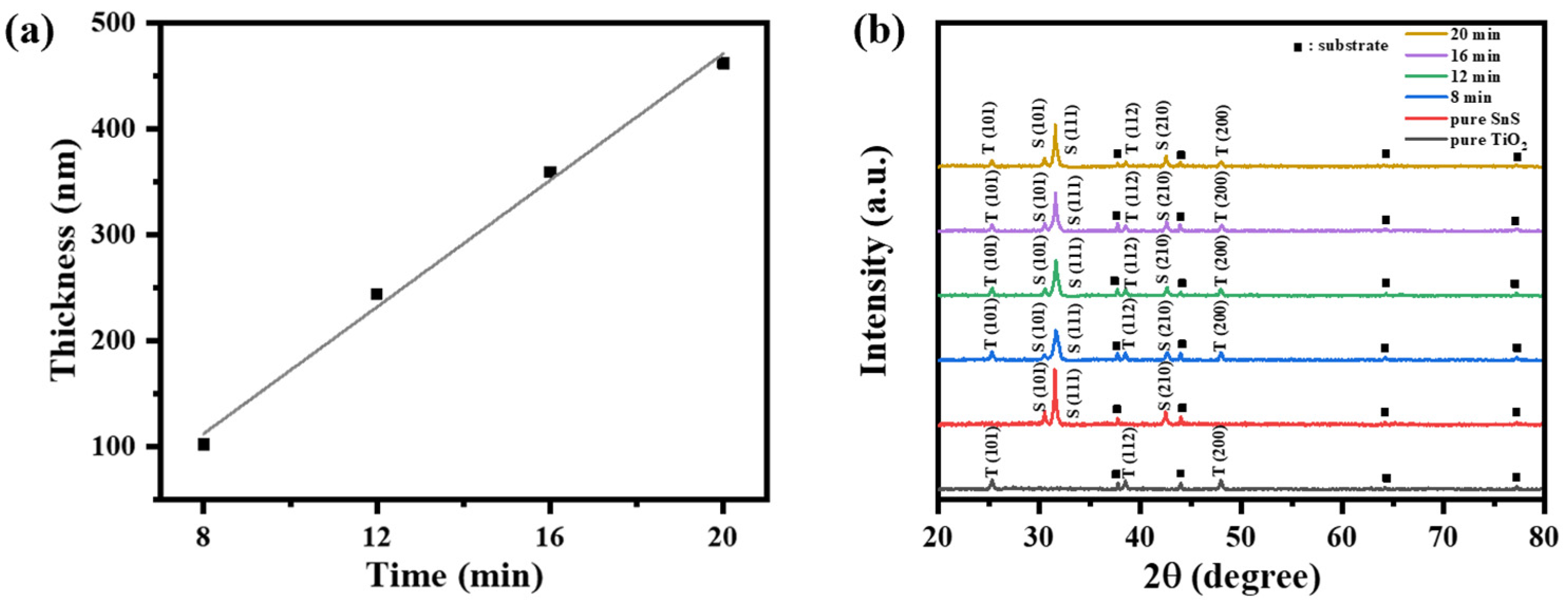
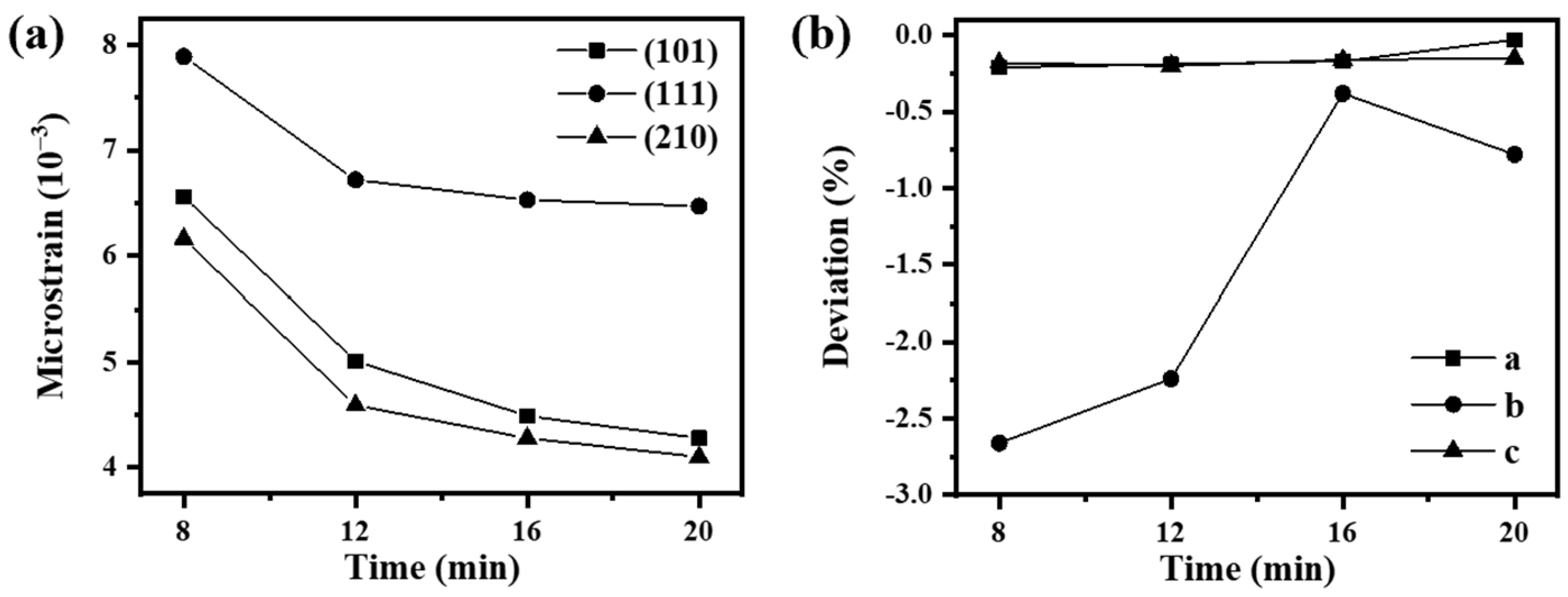
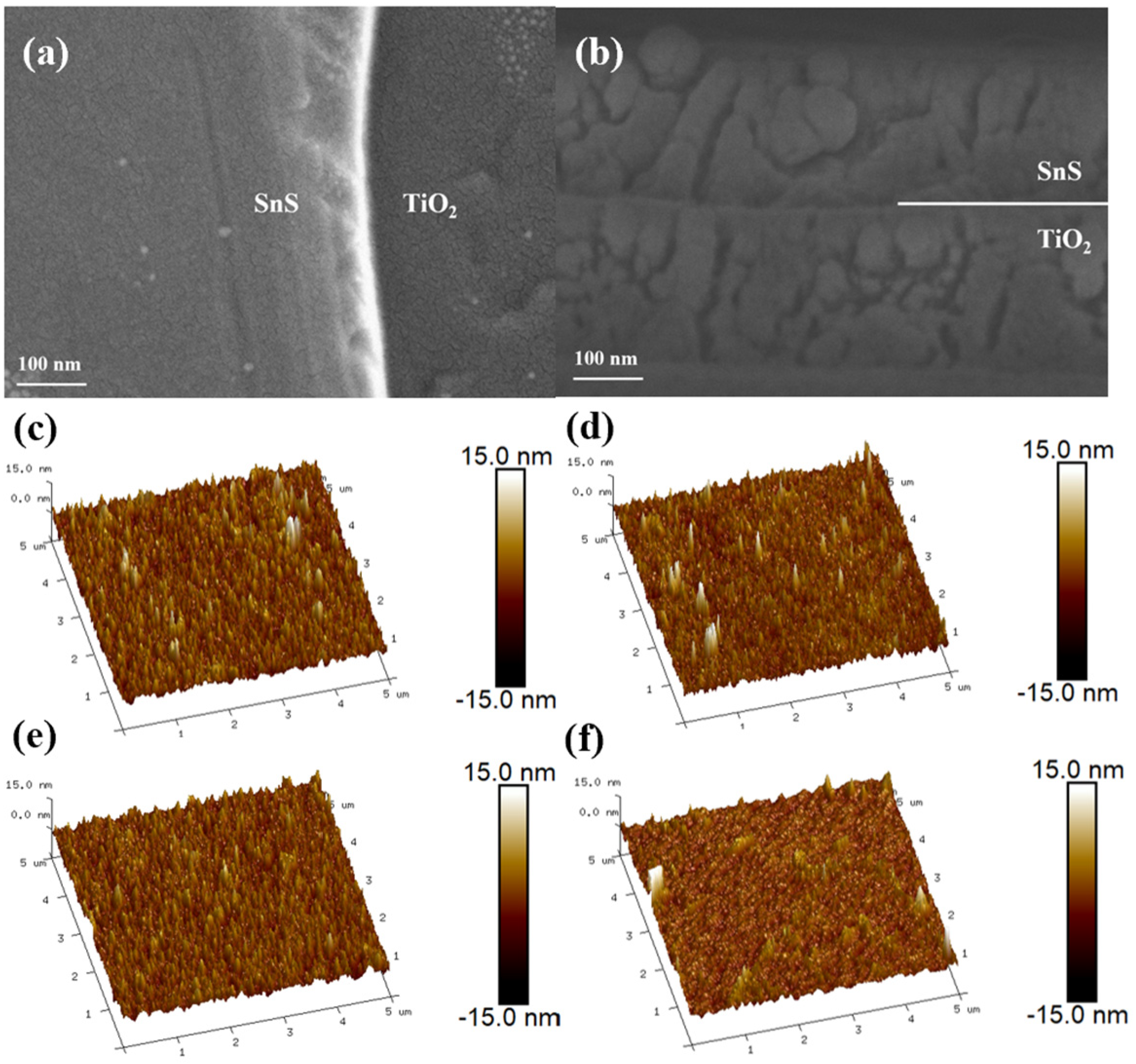
2.1. Structural Characterization

When the sputtering power was fixed at 80 W, the deposition rate typically remained stable. Consequently, the film thickness of SnS generally increased linearly with a prolonged sputtering time. The thicknesses of SnS and TiO2 layers in different samples are shown in Table 1.
The thickness of the TiO2 layer was maintained at approximately 220 nm, while the thickness of SnS layer exhibited a linear dependence on the sputtering time, as shown in Figure 1a. The linear regression analysis yielded a coefficient of determination (R2) of 0.9918, confirming an excellent linear relationship between the thickness of SnS film and deposition time. Specifically, as the sputtering duration increased from 8 to 20 min, the corresponding thickness increased from 102 to 462 nm.
The XRD patterns of the SnS/TiO2 heterostructure, pure SnS, and pure TiO2 thin films are shown in Figure 1b. All SnS/TiO2 films exhibited diffraction peaks corresponding to both SnS and TiO2 phases. As the sputtering time of the SnS layer increased, the diffraction peaks of SnS became more intense while those of TiO2 showed a gradual decrease in intensity. The SnS layers displayed an orthorhombic structure with a polycrystalline nature that matched well with the standard diffraction pattern (JCPDS No. 39-0354), with characteristic peaks observed at approximately 30.52°, 31.60°, and 42.60°, corresponding to the (101), (111), and (210) planes of SnS, respectively. With an increasing sputtering time, the (111) and (210) diffraction peaks shifted slightly toward lower angles, and no diffraction peaks corresponding to impurity phases such as SnS2 or Sn2S3 were detected. Additionally, three diffraction peaks of TiO2 were observed and identified as the anatase phase (JCPDS No. 21-1272), including the (101) plane peak at 25.29°, the (112) plane peak at 38.51°, and the (200) plane peak at 47.97°. The relatively weak intensity of these TiO2 diffraction peaks is likely due to the fact that the TiO2 layer was located beneath the SnS layer and had a relatively small thickness.
The crystallite size (D) and microstrain (ε) of both SnS and TiO2 were calculated using Scherrer’s formula (Equation (1)) and the strain equation (Equation (2)), respectively [43,44]:
D = K λ β c o s θ
ε = β 4 t a n θ
where K is the Scherrer constant, λ denotes the X-ray wavelength (0.15406 nm), β represents the full width at half maximum (FWHM) of the diffraction peak, and θ is the Bragg diffraction angle.
The lattice parameters of both thin films were calculated using Bragg’s law (Equation (3)) and the interplanar spacing formula (Equation (4)) [45], where λ represents the incident X-ray wavelength, dhkl denotes the interplanar spacing, θ is the diffraction angle, (h, k, l) are the Miller indices, and (a, b, c) stand for the lattice constants. SnS crystallizes in the orthorhombic system, while anatase TiO2 adopts a tetragonal structure (with a = b) [46,47]. The calculated crystallite sizes and lattice parameters are summarized in Table 2.
λ = 2 d h k l s i n θ
1 d h k l 2 = ( h a ) 2 + ( k b ) 2 + ( l c ) 2
The TiO2 thin films had a grain size of about 27 nm, with lattice parameters close to standard values (a = b = 3.7852 Å, c = 9.5139 Å). For the SnS films, when the sputtering time increased from 8 to 20 min, the grain size grew from 18.5 nm to 24.6 nm, yet remained smaller than that of pure SnS films deposited directly on glass substrates. The variation in microstrain across different crystallographic planes is illustrated in Figure 2a, showing a consistent decreasing trend in microstrain for all observed planes with an increasing sputtering time. The most significant changes in both grain size and microstrain occurred when the sputtering time increased from 8 to 12 min, with subsequent prolongation showing diminished variation amplitudes. As the film thickness increased, the grains developed more completely through the growth and merging of smaller crystallites, resulting in larger grain sizes and improved crystallinity [48]. The standard lattice parameters for orthorhombic SnS are a = 4.3291 Å, b = 11.1923 Å, and c = 3.9838 Å. The deviations of lattice constants for different samples from standard values are presented in Figure 2b, as determined by the following Equation (5):
δ a = a a 0 a 0 ;   δ b = b b 0 b 0 ;   δ c = c c 0 c 0
Considerable deviations occurred at the shorter sputtering time of 8–12 min, while films deposited for 16–20 min showed better agreement with standard values. This behavior may be attributed to the insufficiently smooth surface of the TiO2 films, which imposed a localized strain on the overlying SnS films and hindered proper grain growth, causing lattice distortion. Additionally, the poor lattice matching between the SnS films and substrate contributed to the deviation of lattice parameters [49].
The morphology of the SnS/TiO2 thin films are shown in Figure 3. Figure 3a,b presents the surface and cross-sectional views of the heterostructure film, respectively, where the SnS layer was deposited for 12 min. The SEM images clearly revealed the heterostructure. Figure 3c–f display the AFM images of various samples, showing that the film surface exhibited enhanced planarity as the SnS sputtering time increased from 8 to 20 min. As shown in Table 3, the root mean square (RMS) roughness ranged from 1.60 to 1.93 nm.
The elemental composition of SnS/TiO2 films prepared with different sputtering times of SnS showed no significant variations. Therefore, representative EDS and XPS spectra from the sample with the 8 min sputtering time of SnS are presented in Figure 4. The EDS spectrum revealed the elemental distribution, with atomic percentages for different samples summarized in Table 4. As the SnS layer thickness increased, the atomic percentages of Sn and S progressively rose, while those of Ti and O correspondingly decreased. In the heterostructure films, the Ti:O ratio was approximately 1:2.12, close to the theoretical value of 1:2. The Sn:S ratio was about 1.23:1, indicating a Sn-rich and S-deficient composition in the SnS films. This deviation primarily arises from the much higher saturated vapor pressure of S compared to Sn, causing the preferential re-evaporation of S atoms from the film surface during deposition.
Due to the shallow probing depth of XPS, the characterization of heterostructure films was conducted in two stages: first, the pure TiO2 film was analyzed to obtain high-resolution spectra of Ti and O elements, shown in Figure 4e,f; subsequently, after the SnS layer deposition, another measurement was performed to determine the elemental composition and chemical states of the SnS film. Figure 4b shows the XPS survey spectrum of the upper SnS layer, while Figure 4c,d presents the high-resolution spectra of Sn and S elements, respectively. In the Sn 3d spectrum, the peaks at 485.5 eV and 494.0 eV corresponded to the Sn 3d5/2 and Sn 3d3/2 energy levels, respectively, with a binding energy difference of 8.5 eV, confirming the presence of Sn2+ [50]. The S 2p spectrum exhibited two peaks at 160.3 eV and 161.5 eV, attributed to the spin–orbit splitting of S2− [51]. Combined with XRD results, it was demonstrated that the phase-pure nature of the magnetron-sputtered SnS layer effectively avoided detrimental effects from impurity phases on the light-absorption properties. Figure 4e,f displays the high-resolution spectra of Ti and O elements from the pure TiO2 film. The Ti 2p spectrum showed characteristic peaks at 458.4 eV of Ti 2p3/2 and 464.1 eV of Ti 2p1/2, with a spin–orbit splitting of 5.7 eV, consistent with Ti4+ [52]. The O 1s spectrum revealed two components: the peak at 529.8 eV originated from Ti-O bonds, while the peak at 531.7 eV was assigned to surface -OH groups [53].
Figure 5a presents the UV-Vis-NIR diffuse reflectance spectra of SnS/TiO2 heterostructure thin films prepared with different sputtering time of SnS. The Tauc equation (Equation (6)) was employed to calculate the bandgaps of both pure SnS and TiO2 films [54,55]:
( α h ν ) 1 n = A ( h ν E g )
α represents the absorption coefficient, A is a constant, and the value of n depends on the electronic transition characteristics of the semiconductor. The direct bandgap of SnS was calculated with n = 1/2, while TiO2, as an indirect bandgap semiconductor, was assigned n = 2 [56,57]. In indirect transitions, the energy contribution from electron–phonon interactions is much smaller than the photon energy. Near the band edges, the influence of phonon energy on the absorption coefficient is relatively weak. Therefore, the phonon energy is approximated as a perturbation to the bandgap and directly incorporated into the effective bandgap value [54,58]. The Tauc plot of the pure SnS and TiO2 film is shown in Figure 5b,c, with the corresponding absorption spectra provided as insets. The pure SnS film, deposited with a sputtering time of 20 min and a thickness of 456 nm, exhibited a bandgap of 1.27 ± 0.03 eV, while the pure TiO2 film with a thickness of 231 nm had a bandgap of 3.26 ± 0.03 eV. The SnS thin film with a narrow bandgap exhibited superior visible-light absorption compared to TiO2. When composited with TiO2 to form the heterostructure, the resulting films demonstrated a pronounced red shift in absorption edge and significantly enhanced the visible-light-absorption capacity. As the sputtering time of SnS layers increased from 8 to 12 min, the films showed substantial improvement in light absorption. However, the further extension of the deposition time yielded diminishing returns, with the 20 min sample displaying a slightly lower absorption than the 16 min counterpart. This thickness-dependent optical behavior can be attributed to several interrelated factors. Thinner films suffer from incomplete photon absorption due to a limited optical path length, while increased thickness promotes more efficient light harvesting through extended propagation paths and improved crystallinity [59]. This improvement correlates with grain growth and structural perfection, which collectively induce bandgap narrowing and broaden the spectral response. Beyond optimal thickness, the absorption efficiency approaches saturation, with potential performance degradation caused by intensified light scattering and reflection losses [60]. Notably, the most significant enhancements in both grain size and light absorption occur during the initial 8 to 12 min of thickness increase, highlighting the critical influence of SnS crystallinity in determining the optical performance of heterostructure system.

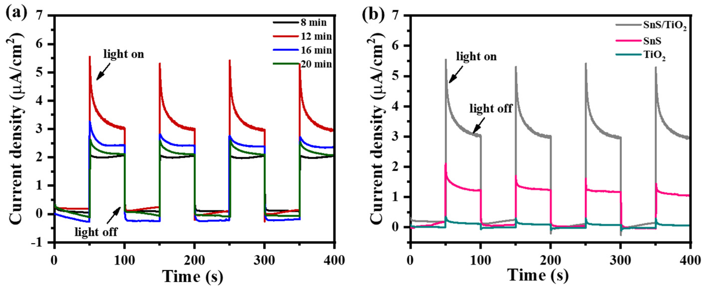
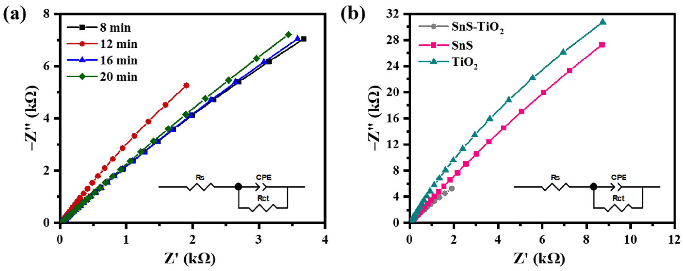
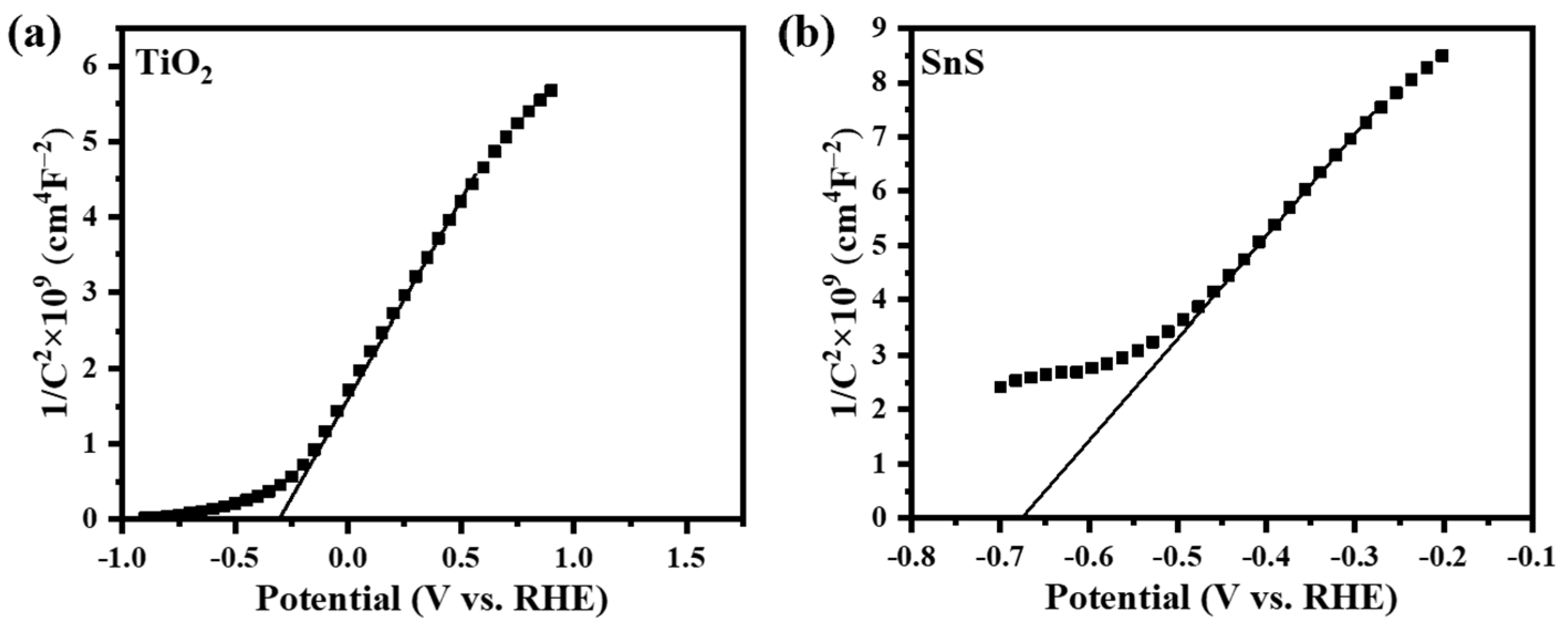
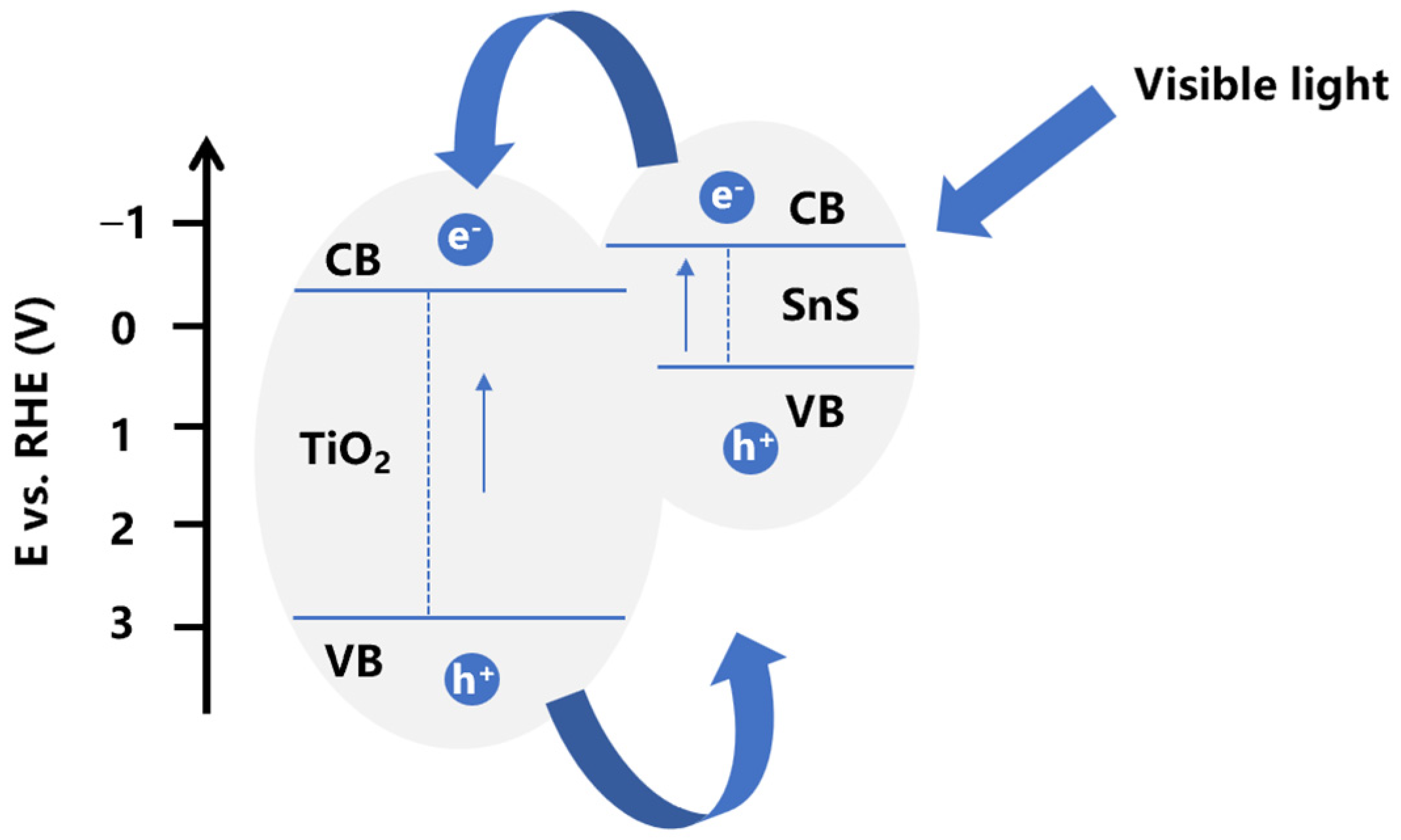
2.2. Photoelectrochemical Characterization

Transient photocurrent tests were performed under visible-light irradiation using SnS/TiO2 heterostructure thin films prepared with different sputtering times of SnS as photoanodes, with the results shown in Figure 6a. When the deposition time of SnS layer increased from 8 to 12 min, the photocurrent density of the heterostructure films exhibited a significant enhancement, rising from 1.98 µA/cm2 to 3.03 µA/cm2. However, the further prolongation of the sputtering time and corresponding increase in the SnS layer thickness led to a noticeable decline in photocurrent generation under visible light, with the 20 min sample showing a photocurrent density comparable to that of the 8 min sample. This phenomenon can be attributed to the improved crystalline quality and structural ordering of SnS layers with increasing thickness, which initially enhances their light-absorption capability. Nevertheless, when the film thickness exceeds an optimal range, the absorption approaches saturation while charge carrier scattering at grain boundaries and interfaces becomes more pronounced, ultimately reducing charge transport efficiency and photocurrent density [60,61]. Pure SnS and TiO2 films of equivalent thickness to the optimized 12 min heterostructure served as controls to demonstrate the photoelectrochemical performance improvement. The current–time curves of these three configurations are presented in Figure 6b. The pure TiO2 film demonstrated a minimal photocurrent density due to its poor visible-light absorption. While the pure SnS film generated a photocurrent density of 1.28 µA/cm2, the optimized heterostructure achieved 3.03 µA/cm2, representing a 13.8-fold enhancement over the pure TiO2 film and a 2.4-fold improvement compared to SnS.
To analyze the differences in photoelectrochemical performance among the various structures, electrochemical impedance spectroscopy (EIS) measurements were conducted to elucidate the charge transport and interfacial reaction mechanisms that may occur in different film architectures. Figure 7 displays the Nyquist plots of the samples, where the impedance (Z) is defined as a standard complex function comprising a real component (Z′) and an imaginary component (Z″) [62]:
Z ω = Z ω + i Z ( ω )
All EIS spectra exhibited semicircular arcs, indicating that the electrochemical processes at the semiconductor/electrolyte interface were primarily controlled by charge transfer [62]. The spectra were fitted using the equivalent circuit shown in the figure, where Rs represents the solution resistance, CPE denotes the constant phase element, and Rct is the charge transfer resistance at the electrode surface. The fitted parameters are listed in Table 5. When the sputtering time of SnS increased from 8 to 12 min, the Rct of the SnS/TiO2 films decreased from 99.85 kΩ to 79.96 kΩ. However, with further increases in sputtering time, the Rct gradually rose to 168.33 kΩ, demonstrating that the interfacial charge transfer efficiency initially improved but subsequently deteriorated with an increasing SnS layer thickness. To further investigate the kinetics of the relevant electrochemical processes, the electron transfer rate constant (k0) at the film/electrolyte interface was calculated using Equation (8) [62]:
k 0 = R T n 2 F 2 A R c t C
where R, T, and n represent the universal gas constant, reaction temperature, and number of electrons involved in the S2−/S redox reaction, respectively, F denotes the Faraday constant (~96,485 C/mol), A is the electrode surface area, and C is the concentration of the S2−/S redox couple in solution.
The exchange current density (J0) was additionally calculated using Equation (9) [63], with the results listed in Table 5:
J 0 = R T n F R c t
When the SnS layer was deposited for 12 min, the heterostructure film achieved maximum values for both k0 of 1.637 × 10⁻⁸ m/s and J0 of 1.580 × 10⁻⁷ A/cm2, demonstrating that an optimal SnS thickness can significantly enhance the charge transfer efficiency. However, when the sputtering time exceeded 12 min, both k0 and J0 decreased, likely because the increased thickness of the light-absorption layer began to adversely affect charge carrier transport pathways, thereby elevating recombination probability [64].
The pure SnS and TiO2 films of equivalent thickness exhibited Rct values of 523.53 kΩ and 289.52 kΩ, respectively. In contrast, the heterostructure demonstrated significantly reduced Rct values, accompanied by substantially enhanced k0 and J0 values. To further investigate the charge transfer facilitation mechanism in the heterojunction, a Mott–Schottky (M-S) analysis was performed on both SnS and TiO2 films, with the resulting curves presented in Figure 8. Equation (10) is as follows [65]:
1 C S C 2 = 2 e ε r ε 0 N D ( V V f b k B T e )
where Csc represents the space charge layer capacitance, εr is the relative dielectric constant of the semiconductor, ε0 denotes the vacuum permittivity, e is the elementary charge, ND stands for the donor concentration, V is the applied potential, Vfb indicates the flat-band potential, kB is the Boltzmann constant, and T is the temperature. The flat-band potentials (Vfb vs. RHE) of the TiO2 and SnS films were determined to be −0.31 V and −0.67 V, respectively, by extrapolating the linear portion of the M-S curves to the intercept with the x-axis. For n-type semiconductors, the conduction band potential (ECB vs. RHE) can be approximated as the Vfb (vs. RHE) [66]. Combined with the bandgap values obtained from UV-Vis-NIR spectroscopy, the valence band potentials (EVB vs. RHE) were calculated using Equation (11) [67]:
E V B = E C B + E g
The calculated (EVB vs. RHE) of the TiO2 and SnS thin films were 2.95 V and 0.60 V, respectively. Based on these results, the energy band diagrams of TiO2 and SnS were constructed, as shown in Figure 9. Under visible-light irradiation, electrons in SnS were excited from the valence band to the conduction band. The formation of a type-II heterojunction between TiO2 and SnS facilitated the directional charge carrier migration, where photogenerated electrons were transferred from the conduction band of SnS to TiO2, while holes migrated toward and accumulated in the valence band of SnS [10]. This spatial separation of electrons and holes not only enhanced the charge separation efficiency but also intensified the upward band bending at the SnS/electrolyte interface [35,68]. As a result, hole injection into the electrolyte was promoted, accelerating interfacial oxidation reactions. Consequently, the charge transfer resistance (Rct) at the semiconductor/electrolyte interface was significantly reduced, indicating markedly improved charge transfer kinetics.
Photocatalytic degradation tests of methylene blue were conducted on the 12 min sputtered SnS/TiO2 heterostructure film along with pure SnS and TiO2 films of equivalent thickness. For first-order reactions, the photocatalytic rate constant can be calculated using the following equation [69,70]:
ln C 0 C = k t
The photocatalytic degradation kinetics were analyzed using the first-order reaction model, where C0 represents the initial solution concentration, C is the concentration after irradiation time t, and k denotes the reaction rate constant. Figure 10a plots the −ln(C/C0) values versus time for all samples, with the fitted R2 values and k rate constants summarized in Table 6. The R2 values exceeding 0.99 confirmed that the photocatalytic degradation followed first-order kinetics for all samples. The pure SnS and TiO2 films exhibited relatively low-rate constants, attributable to the poor visible-light absorption of TiO2 and the rapid charge recombination of SnS, despite its strong visible-light harvesting capability. In contrast, the SnS/TiO2 heterostructure film achieved the highest rate constant of 0.0170, demonstrating superior catalytic performance with 87% methylene blue degradation within 120 min under visible light. The reproducibility testing of SnS/TiO2 demonstrated consistent performance across three successive cycles, as illustrated in Figure 10b. The rate constants for the second and third cycles were determined to be 0.0157 and 0.0151, respectively, while the third cycle achieved 84% degradation efficiency for methylene blue. The degradation mechanism likely involved the generation of reactive oxygen species such as hydroxyl radicals (OH) and superoxide radicals (O2−•) through redox reactions, as reported in similar photocatalytic systems [71,72,73]. These active species were responsible for the oxidative breakdown of the dye molecules.
The SnS/TiO2 heterostructure demonstrated superior photoelectrochemical performance compared to its individual counterparts due to synergistic interactions across multiple stages [74]. Under visible-light irradiation, the narrow bandgap of SnS enabled efficient light absorption [27]. The type-II band alignment played a crucial role by facilitating charge separation, where photogenerated electrons in SnS transferred to the TiO2 conduction band due to its more negative potential, while holes migrated to the SnS valence band, thereby effectively suppressing recombination and improving charge transport efficiency [69]. Additionally, the heterojunction interface likely contained unique active sites such as defect states that further enhanced redox reaction kinetics [75]. These combined effects achieved photocatalytic performance comparable to other TiO2-based catalysts reported in other works such as N-doped TiO2 [76], CdS/TiO2 [20], and Cu2O/TiO2 [25] systems.

3. Materials and Methods

3.1. Preparation of SnS/TiO2 Heterostructure Thin Films

SnS/TiO2 heterostructure thin films were prepared using a vacuum deposition equipment (SY-500, Beijing Shengdeyu Vacuum Technology Co., Ltd., Beijing, China). Glass slides were used as substrates and sequentially cleaned by ultrasonication in acetone, absolute ethanol, and deionized water for 10 min each. TiO2 thin films were deposited by radio-frequency magnetron sputtering using a TiO2 target (99.99%, ZhongNuo Advanced Material Technology Co., Ltd., Beijing, China) with a sputtering power of 300 W for 30 min. During deposition, the Ar flow rate was maintained constant at 70 sccm with a working pressure of 0.55 Pa. The as-deposited TiO2 films were then annealed in a tube furnace at 500 °C for 2 h in air. In our previous work, the preparation process of SnS thin films was optimized, including parameters such as sputtering power, annealing time, and annealing temperature. Subsequently, SnS thin films were deposited on the TiO2 films by radio-frequency magnetron sputtering using a SnS target (99.99%, ZhongNuo Advanced Material Technology Co., Ltd., Beijing, China) with a constant sputtering power of 80 W. The sputtering time varied between 8, 12, 16, and 20 min for different samples. A final annealing process was performed in the tube furnace at 300 °C for 1 h under Ar atmosphere to complete the preparation of SnS/TiO2 heterostructure thin films.

3.2. Characterization and Measurements

The crystal structure and phase composition of the samples were characterized by X-ray diffraction (Bruke D8 with Cu-Kα radiation, Billerica, MA, USA). Scanning electron microscopy (SEM) (ZEISS Gemini 300, Jena, Germany) and atomic force microscopy (AFM) (Bruker Dimension ICON, Billerica, MA, USA) were employed to analyze the surface and cross-sectional morphology. X-ray photoelectron spectroscopy (XPS) (Thermo Scientific K-Alpha, Waltham, MA, USA) was used to determine the elemental composition and chemical states of the thin films. The optical absorption properties were evaluated using ultraviolet-visible-near infrared (UV-Vis-NIR) spectrophotometry (Shimadzu UV-3600, Kyoto, Japan).
The photoelectrochemical performance of the samples was tested using a three-electrode system connected to an electrochemical workstation (CHI660E) at room temperature. The three-electrode system consisted of a working electrode (the thin-film samples deposited on FTO glass with an effective area of 1 cm2), a reference electrode (saturated calomel electrode, SCE), and a counter electrode (Pt disk electrode). A xenon lamp served as the light source, equipped with an optical filter to control the visible-light wavelength range between 420 and 780 nm, delivering an irradiance of 62 mW/cm2 at the sample surface. The measurements were conducted in a 0.5 mol/L Na2SO4 aqueous electrolyte solution (pH = 7). All measured potentials were converted to the reversible hydrogen electrode (RHE) scale using the Nernst equation (Equation (13)) [77], where ERHE represents the potential relative to the reversible hydrogen electrode (RHE), ESCE is the potential measured against the saturated calomel electrode (SCE), and E S C E θ denotes the standard electrode potential of SCE:
E R H E = E S C E + 0.0591 p H + E S C E θ ( E S C E θ = 0.2415   v s .   N H E   a t   25   ° C )
For transient photocurrent tests, an open-circuit potential was applied to the working electrode while recording current–time profiles under alternating light-on and light-off conditions. Each state (illuminated/non-illuminated) was maintained for 50 s, with a total test duration of 400 s. Electrochemical impedance spectroscopy (EIS) was performed under visible-light irradiation across a frequency range of 0.1 Hz to 100,000 Hz. A Mott–Schottky analysis was conducted in dark conditions at a fixed frequency of 1000 Hz with an AC amplitude of 10 mV.
The photocatalytic degradation performance of the thin films was evaluated using a methylene blue (MB) dye solution as the model pollutant. A film sample with a surface area of 1 × 1 cm2 was immersed in 50 mL of MB aqueous solution (4 mg/L), consistent with our previous work [78]. Prior to illumination, the reactor was placed on a magnetic stirrer and kept in dark conditions for 30 min to establish adsorption–desorption equilibrium on the catalyst surface. During the photocatalytic test, the sample was irradiated with visible light from a xenon lamp positioned at a distance of 30 cm. Aliquots of 4 mL were collected at 20 min intervals over a total irradiation period of 120 min. The concentration of MB in each collected sample was immediately determined using an ultraviolet-visible spectrophotometer (UV-2300, Shanghai Techcomp Instruments Ltd., Shanghai, China).

4. Conclusions

SnS/TiO2 heterostructure thin films were fabricated by RF magnetron sputtering with a fixed TiO2 thickness of 225 nm and varying SnS deposition times. The characterization confirmed phase-pure SnS layers, with optimal optoelectronic performance at a 244 nm SnS thickness. The increased SnS thickness enhanced crystallinity, grain growth, and light absorption, but excessive thickness led to absorption saturation and reduced charge transport due to carrier scattering. The 12 min SnS sputtered heterostructure thin film exhibited a maximum photocurrent density of 3.03 µA/cm2 under visible light, which was 13.8 times that of pure TiO2 thin film and 2.4 times that of pure SnS thin film with an equivalent thickness. This enhancement arose from the following: (1) the narrow-bandgap SnS effectively extended the light absorption; (2) the type-II band alignment promoted charge separation. Photocatalytic tests showed 87% methylene blue degradation in 120 min, far outperforming pure SnS and TiO2 films. These results demonstrated the feasibility of using a purely physical method for constructing SnS/TiO2 heterojunctions with tunable structural parameters and controlled interface quality. Additionally, further investigations are required to examine the influence of pH values and initial pollutant concentrations on the degradation rate, as well as to explore the degradation mechanism through radical trapping experiments and byproduct analysis.

Author Contributions

Conceptualization, Y.D. and J.S.; methodology, Y.D.; validation, Y.D., J.L. and M.Z.; formal analysis, Y.D. and J.L.; investigation, Y.D., J.L. and M.Z.; writing—original draft preparation, Y.D. and J.S.; writing—review and editing, Y.D. and J.S.; supervision, J.S.; project administration, J.S.; funding acquisition, J.S. All authors have read and agreed to the published version of the manuscript.

Funding

This work was supported by the Natural Science Foundation of China (No. 61671155).

Institutional Review Board Statement

Not applicable.

Informed Consent Statement

Not applicable.

Data Availability Statement

The original contributions presented in this study are included in the article. Further inquiries can be directed to the corresponding author.

Acknowledgments

The authors express gratitude to the Department of Materials Science in Fudan University for the magnetron sputtering equipment. Additionally, special thanks are extended to Xiaoli Cui for her guidance and assistance during the photoelectrochemical characterization.

Conflicts of Interest

The authors declare no conflicts of interest.

References

  1. Arun, J.; Nachiappan, S.; Rangarajan, G.; Alagappan, R.P.; Gopinath, K.P.; Lichtfouse, E. Synthesis and application of titanium dioxide photocatalysis for energy, deconta ination and viral disinfection: A review. Environ. Chem. Lett. 2023, 21, 339–362. [Google Scholar] [CrossRef]
  2. Liu, Y.; Li, Z.; Green, M.; Just, M.; Li, Y.Y.; Chen, X.B. Titanium dioxide nanomaterials for photocatalysis. J. Phys. D Appl. Phys. 2017, 50, 193003. [Google Scholar] [CrossRef]
  3. Chen, D.J.; Cheng, Y.L.; Zhou, N.; Chen, P.; Wang, Y.P.; Li, K.; Huo, S.H.; Cheng, P.F.; Peng, P.; Zhang, R.C. Photocatalytic degradation of organic pollutants using TiO2-based photocatalysts: A review. J. Clean. Prod. 2020, 268, 121725. [Google Scholar] [CrossRef]
  4. Shu, Z.X.; Jiao, X.L.; Chen, D.R. Synthesis and photocatalytic properties of flower-like zirconia nanostructures. Cryst. Eng. Comm. 2012, 14, 1122–1127. [Google Scholar] [CrossRef]
  5. Chu, M.N.; Hu, K.; Wang, J.S.; Liu, Y.D.; Ali, S.; Qin, C.L.; Jing, L.Q. Synthesis of g-C3N4-based photocatalysts with recyclable feature for efficient 2,4-dichlorophenol degradation and mechanisms. Appl. Catal. B 2019, 243, 57–65. [Google Scholar] [CrossRef]
  6. Hu, J.S.; Ren, L.L.; Guo, Y.G.; Liang, H.P.; Cao, A.M.; Wan, L.J.; Bai, C.L. Mass production and high photocatalytic activity of ZnS nanoporous nanoparticles. Angew. Chem. Int. Ed. 2005, 44, 1269–1273. [Google Scholar] [CrossRef]
  7. Wu, G.L.; Li, P.; Xu, D.B.; Luo, B.F.; Hong, Y.Z.; Shi, W.D.; Liu, C.B. Hydrothermal synthesis and visible-light-driven photocatalytic degradation for tetracycline of Mn-doped SrTiO3 nanocubes. Appl. Surf. Sci. 2015, 333, 39–47. [Google Scholar] [CrossRef]
  8. Gopidas, K.R.; Bohorquez, M.; Kamat, P.V. Photophysical and photochemical aspects of coupled semiconductors: Charge-transfer processes in colloidal cadmium sulfide-titania and cadmium sulfide-silver(I) iodide systems. J. Phys. Chem. 1990, 94, 6435–6440. [Google Scholar] [CrossRef]
  9. Khanchandani, S.; Kundu, S.; Patra, A.; Ganguli, A.K. Band gap tuning of ZnO/In2S3 core/shell nanorod arrays for enhanced visible-light-driven photocatalysis. J. Phys. Chem. C 2013, 117, 5558–5567. [Google Scholar] [CrossRef]
  10. He, X.H.; Kai, T.H.; Ding, P. Heterojunction photocatalysts for degradation of the tetracycline antibiotic: A review. Environ. Chem. Lett. 2021, 19, 4563–4601. [Google Scholar] [CrossRef]
  11. Yuan, X.Z.; Jiang, L.B.; Liang, J.; Pan, Y.; Zhang, J.; Wang, H.; Leng, L.J.; Wu, Z.B.; Guan, R.P.; Zeng, G.M.; et al. In-situ synthesis of 3D microsphere-like In2S3/InVO4 heterojunction with efficient photocatalytic activity for tetracycline degradation under visible light irradiation. Chem. Eng. J. 2019, 356, 371–381. [Google Scholar] [CrossRef]
  12. Leary, R.; Westwood, A. Carbonaceous nanomaterials for the enhancement of TiO2 photocatalysis. Carbon 2011, 49, 741–772. [Google Scholar] [CrossRef]
  13. Ahmad, M.; Ghafoor, A.; Haoran, S.; Ali, U.; Meng, X.L.; Kamara, A.; Nazir, A.; Jie, Z.; Liu, Z.; Yan, Z.F. Acquiescent tailoring of TiO2 band gap via surged NiSe NPs decoration for accelerated photocatalytic degradation of methyl orange. J. Water Process Eng. 2025, 70, 107001. [Google Scholar] [CrossRef]
  14. Rashid, R.; Shafiq, I.; Gilani, M.R.H.S.; Maaz, M.; Akhter, P.; Hussain, M.; Jeong, K.; Kwon, E.E.; Bae, S.; Park, Y. Advancements in TiO2-based photocatalysis for environmental remediation: Strategies for enhancing visible-light-driven activity. Chemosphere 2024, 349, 140703. [Google Scholar] [CrossRef]
  15. Cui, F.M.; Hua, Z.L.; Wei, C.Y.; Li, J.Q.; Gao, Z.; Shi, J.L. Highly dispersed Au nanoparticles incorporated mesoporous TiO2 thin films with ultrahigh Au content. J. Mater. Chem. 2009, 19, 7632–7637. [Google Scholar] [CrossRef]
  16. Naseri, N.; Kim, H.; Choi, W.; Moshfegh, A.Z. Optimal Ag concentration for H2 production via Ag:TiO2 nanocomposite thin film photoanode. Int. J. Hydrogen Energy 2012, 37, 3056–3065. [Google Scholar] [CrossRef]
  17. Wang, X.X.; Zhao, J.L.; Kang, Y.R.; Li, L.L.; Xu, X.R. Photoelectrochemical properties of Fe-doped TiO2 nanotube arrays fabricated by anodization. J. Appl. Electrochem. 2014, 44, 1–4. [Google Scholar] [CrossRef]
  18. Guo, W.; Shen, Y.H.; Wu, L.Q.; Gao, Y.R.; Ma, T.L. Effect of N dopant amount on the performance of dye-Sensitized solar cells based on N-doped TiO2 electrodes. J. Phys. Chem. C 2011, 115, 21494–21499. [Google Scholar] [CrossRef]
  19. Giannakas, A.E.; Antonopoulou, M.; Daikopoulos, C.; Deligiannakis, Y.; Konstantinou, I. Characterization and catalytic performance of B-doped, B–N co-doped and B–N–F tri-doped TiO2 towards simultaneous Cr(VI) reduction and benzoic acid oxidation. Appl. Catal. B Environ. 2016, 184, 44–54. [Google Scholar] [CrossRef]
  20. Zhao, W.X.; Bai, Z.P.; Ren, A.L.; Guo, B.; Wu, C. Sunlight photocatalytic activity of CdS modified TiO2 loaded on activated carbon fibers. Appl. Surf. Sci. 2010, 256, 3493–3498. [Google Scholar] [CrossRef]
  21. Han, H.; Riboni, F.; Karlicky, F.; Kment, S.; Goswami, A.; Sudhagar, P.; Yoo, J.; Wang, L.; Tomanec, O.; Petr, M.; et al. α-Fe2O3/TiO2 3D hierarchical nanostructures for enhanced photoelectrochemical water splitting. Nanoscale 2017, 9, 134–142. [Google Scholar] [CrossRef]
  22. Wang, C.C.; Zhan, Y.; Wang, Z.Y. TiO2, MoS2, and TiO2/MoS2 heterostructures for use in organic dyes degradation. Chem. Sel. 2018, 3, 1713–1718. [Google Scholar] [CrossRef]
  23. Wang, G.M.; Wang, H.Y.; Ling, Y.C.; Tang, Y.C.; Yang, X.Y.; Fitzmorris, R.C.; Wang, C.C.; Zhang, J.Z.; Li, Y. Hydrogen-treated TiO2 nanowire arrays for photoelectrochemical water splitting. Nano Lett. 2011, 11, 3026–3033. [Google Scholar] [CrossRef]
  24. Yan, M.; Li, G.L.; Guo, C.S.; Guo, W.; Ding, D.D.; Zhang, S.H.; Liu, S.Q. WO3-x sensitized TiO2 spheres with full-spectrum-driven photocatalytic activities from UV to near infrared. Nanoscale 2016, 8, 17828–17835. [Google Scholar] [CrossRef]
  25. Adamu, H.; McCue, A.J.; Taylor, R.S.F.; Manyar, H.G.; Anderson, J.A. Simultaneous photocatalytic removal of nitrate and oxalic acid over Cu2O/TiO2 and Cu2O/TiO2-AC composites. Appl. Catal. B Environ. 2017, 217, 181–191. [Google Scholar] [CrossRef]
  26. Wang, Y.Y.; Yang, W.J.; Chen, X.J.; Wang, J.; Zhu, Y.F. Photocatalytic activity enhancement of core-shell structure g-C3N4@TiO2 via controlled ultrathin g-C3N4 layer. Appl. Catal. B Environ. 2018, 220, 337–347. [Google Scholar] [CrossRef]
  27. Kumar, V.; Goswami, Y.C. Ultrasound-assisted facile synthesis of tin sulfide (SnS) nanostructures and their structural, optical, and morphological studies. Phosphorus Sulfur Silicon Relat. Elem. 2025, 200, 405–412. [Google Scholar] [CrossRef]
  28. Kawamura, F.; Song, Y.; Murata, H.; Tampo, H.; Nagai, T.; Koida, T.; Imura, M.; Yamada, N. Tunability of the bandgap of SnS by variation of the cell volume by alloying with AE elements. Sci. Rep. 2022, 12, 7434. [Google Scholar] [CrossRef]
  29. Reddy, N.K.; Devika, M.; Gopal, E.S.R. Review on tin (II) sulfide (SnS) material: Synthesis, properties, and applications. Crit. Rev. Solid State Mater. Sci. 2015, 40, 359–398. [Google Scholar] [CrossRef]
  30. Norton, K.J.; Alam, F.; Lewis, D.J. A review of the synthesis, properties, and applications of bulk and two-dimensional tin (II) sulfide(SnS). Appl. Sci. 2021, 11, 2062. [Google Scholar] [CrossRef]
  31. Nengzi, L.C.; Yang, H.; Hu, J.Z.; Zhang, W.M.; Jiang, D.A. Fabrication of SnS/TiO2 NRs/NSs photoelectrode as photoactivator of peroxymonosulfate for organic pollutants elimination. Sep. Purif. Technol. 2020, 249, 117172. [Google Scholar] [CrossRef]
  32. He, H.Y.; Lu, J.; Cao, L.Y.; Li, M. Photodegradation of methyl orange from wastewater on TiO2/SnS combined powders. Res. Chem. Intermed. 2012, 38, 537–547. [Google Scholar] [CrossRef]
  33. Zhang, X.Y.; Gao, Y.J.; Nengzi, L.C.; Li, B.; Gou, J.F.; Cheng, X.W. Synthesis of SnS/TiO2 nano-tube arrays photoelectrode and its high photoelectrocatalytic performance for elimination of 2,4,6-trichlorophenol. Sep. Purif. Technol. 2019, 228, 115742. [Google Scholar] [CrossRef]
  34. Xu, F.; Scaramuzza, N.; Versace, C. Decorating TiO2 nanoparticle thin film with SnSx(x<1): Preparation, characterization, and photocatalytic activity. Coatings 2024, 14, 1185. [Google Scholar]
  35. Jia, Y.F.; Yang, F.; Cai, F.G.; Cheng, C.H.; Zhao, Y. Photoelectrochemical and charge transfer properties of SnS/TiO2 heterostructure nanotube arrays. Electron. Mater. Lett. 2013, 9, 287–291. [Google Scholar] [CrossRef]
  36. Mittal, A.; Sharma, S.; Kumar, T.; Chauhan, N.S.; Kumari, K.; Maken, S.; Kumar, N. Surfactant-assisted hydrothermally synthesized novel TiO2/SnS@Pd nano-composite: Structural, morphological and photocatalytic activity. J. Mater. Sci. Mater. Electron. 2020, 31, 2010–2021. [Google Scholar] [CrossRef]
  37. Wang, Y.; Gong, H.; Fan, B.H.; Hu, G.X. Photovoltaic behavior of nanocrystalline SnS/TiO2. J. Phys. Chem. C 2010, 114, 3256–3259. [Google Scholar] [CrossRef]
  38. Al Ahmed, S.R. Investigation on the performance enhancement of heterojunction SnS thin-film solar cell with a Zn3P2 hole transport layer and a TiO2 electron transport layer. Energy Fuels 2024, 38, 1462–1476. [Google Scholar] [CrossRef]
  39. Ranjith, K.S.; Maleki, R.; Ghoreishian, S.M.; Mohammadi, A.; Raju, G.S.R.; Huh, Y.S.; Han, Y.K. Defective phase engineering of S-scheme TiO2-SnS/SnS2 core-shell photocatalytic nanofibers for elevated visible light responsive H2 generation and nitrogen fixation. J. Mater. Chem. A 2024, 12, 33818–33833. [Google Scholar] [CrossRef]
  40. Qiu, P.L.; Qin, Y.X.; Xia, Q. Ultrasensitive gas sensor developed from SnS/TiO2-based memristor for dilute methanol detection at room temperature. Sens. Actuators B Chem. 2023, 392, 134038. [Google Scholar] [CrossRef]
  41. Burton, L.A.; Walsh, A. Phase stability of the earth-abundant tin sulfides SnS, SnS2, and Sn2S3. J. Phys. Chem. C 2012, 116, 24262–24267. [Google Scholar] [CrossRef]
  42. Lim, D.; Suh, H.; Suryawanshi, M.; Song, G.Y.; Cho, J.Y.; Kim, J.H.; Jang, J.H.; Jeon, C.W.; Cho, A.; Ahn, S.; et al. Kinetically controlled growth of phase-pure SnS absorbers for thin film solar cells: Achieving efficiency near 3% with long-term stability using an SnS/CdS heterojunction. Adv. Energy Mater. 2018, 8, 1702605. [Google Scholar] [CrossRef]
  43. Guneri, E.; Ulutas, C.; Kirmizigul, F.; Altindemir, G.; Gode, F.; Gumus, C. Effect of deposition time on structural, electrical, and optical properties of SnS thin films deposited by chemical bath deposition. Appl. Surf. Sci. 2010, 257, 1189–1195. [Google Scholar] [CrossRef]
  44. Hase, Y.; Sharma, V.; Doiphode, V.; Waghmare, A.; Punde, A.; Shinde, P.; Shah, S.; Rahane, S.; Vairale, P.; Bade, B.; et al. Humidity sensor properties of hydrothermally grown rutile-TiO2 microspheres on interdigital electrodes (IDEs). J. Mater. Sci. Mater. Electron. 2022, 33, 11825–11840. [Google Scholar] [CrossRef]
  45. Kul, M. Electrodeposited SnS film for photovoltaic applications. Vacuum 2014, 107, 213–218. [Google Scholar] [CrossRef]
  46. Daghrir, R.; Drogui, P.; Robert, D. Modified TiO2 for environmental photocatalytic applications: A review. Ind. Eng. Chem. Res. 2013, 52, 3581–3599. [Google Scholar] [CrossRef]
  47. Voznyi, A.; Kosyak, V.; Grase, L.; Vecstaudza, J.; Onufrijevs, P.; Yeromenko, Y.; Medvid’, A.; Opanasyuk, A. Formation of SnS phase obtained by thermal vacuum annealing of SnS2 thin films and its application in solar cells. Mater. Sci. Semicond. Process. 2018, 79, 32–39. [Google Scholar] [CrossRef]
  48. Kumari, T.P.; Raja, M.M.; Kumar, A.; Srinath, S.; Kamat, S.V. Effect of thickness on structure, microstructure, residual stress and soft magnetic properties of DC sputtered Fe65Co35 soft magnetic thin films. J. Magn. Magn. Mater. 2014, 365, 93–99. [Google Scholar] [CrossRef]
  49. Bashkirov, S.A.; Gremenok, V.F.; Ivanov, V.A.; Shevtsova, V.V.; Gladyshev, P.P. Influence of substrate material on the microstructure and optical properties of hot wall deposited SnS thin films. Thin Solid Film. 2015, 585, 40–44. [Google Scholar] [CrossRef]
  50. Baby, B.H.; Mohan, D.B. The effect of in-situ and post deposition annealing towards the structural optimization studies of RF sputtered SnS and Sn2S3 thin films for solar cell application. Sol. Energy 2019, 189, 207–218. [Google Scholar] [CrossRef]
  51. Reddy, V.R.M.; Gedi, S.; Park, C.; Miles, R.W.; Reddy, K.T.R. Development of sulphurized SnS thin film solar cells. Curr. Appl. Phys. 2015, 15, 588–598. [Google Scholar] [CrossRef]
  52. Deng, J.L.; Gao, J.; Liu, M.; Wang, Y.F.; Zheng, L.C.; Li, Y.; Liu, Y. SnS nanoparticles and MoS2 nanosheets co-decorated TiO2 nanorod film with remarkable photocatalytic and photoelectrochemical properties. J. Electrochem. Soc. 2022, 169, 056513. [Google Scholar] [CrossRef]
  53. Xue, D.N.; Luo, J.; Li, Z.; Yin, Y.L.; Shen, J. Enhanced photoelectrochemical properties from Mo-doped TiO2 nanotube arrays film. Coatings 2020, 10, 75. [Google Scholar] [CrossRef]
  54. Tauc, J.; Grigorov, R.; Vancu, A. Optical properties and electronic structure of amorphous germanium. Phys. Status Solidi 1966, 15, 627. [Google Scholar] [CrossRef]
  55. Coulter, J.B.; Birnie, D.P. Assessing Tauc plot slope quantification: ZnO thin films as a model system. Phys. Status Solidi B 2018, 255, 1700393. [Google Scholar] [CrossRef]
  56. Araújo, M.M.; Silva, L.K.R.; Sczancoski, J.C.; Orlandi, M.O.; Longo, E.; Santos, A.G.D.; Sá, J.L.S.; Santos, R.S.; Luz, G.E.; Cavalcante, L.S. Anatase TiO2 nanocrystals anchored at inside of SBA-15 mesopores and their optical behavior. Appl. Surf. Sci. 2016, 389, 1137–1147. [Google Scholar] [CrossRef]
  57. Sharma, P.K.; Cortes, M.A.L.R.M.; Hamilton, J.W.J.; Han, Y.S.; Byrne, J.A.; Nolan, M. Surface modification of TiO2 with copper clusters for band gap narrowing. Catal. Today 2019, 321, 9–17. [Google Scholar] [CrossRef]
  58. Klein, J.; Kampermann, L.; Mockenhaupt, B.; Behrens, M.; Strunk, J.; Bacher, G. Limitations of the Tauc plot method. Adv. Funct. Mater. 2023, 33, 2304523. [Google Scholar] [CrossRef]
  59. Liu, W.J.; Liu, M.L.; Wang, X.T.; Shen, T.; Chang, G.Q.; Lei, M.; Deng, H.X.; Wei, Z.M.; Wei, Z.Y. Thickness-dependent ultrafast photonics of SnS2 nanolayers for optimizing fiber lasers. ACS Appl. Nano Mater. 2019, 2, 2697–2705. [Google Scholar] [CrossRef]
  60. Javed, A.; Khan, N.; Bashir, S.; Ahmad, M.; Bashir, M. Thickness dependent structural, electrical and optical properties of cubic SnS thin films. Mater. Chem. Phys. 2020, 246, 122831. [Google Scholar] [CrossRef]
  61. Huang, L.Y.; Meng, L. Effects of film thickness on microstructure and electrical properties of the pyrite films. Mater. Sci. Eng. B 2007, 137, 310–314. [Google Scholar] [CrossRef]
  62. Mishra, S.K.; Kumar, D.; Biradar, A.M.; Rajesh. Electrochemical impedance spectroscopy characterization of mercaptopropionic acid capped ZnS nanocrystal based bioelectrode for the detection of the cardiac biomarker-myoglobin. Bioelectrochemistry 2012, 88, 118–126. [Google Scholar] [CrossRef]
  63. Li, P.J.; Zhang, Y.G.; Yang, X.G.; Gao, Y.H.; Ge, S.X. Alloyed PtNi counter electrodes for high-performance dye-sensitized solar cell applications. J. Alloys Compd. 2017, 725, 1272–1281. [Google Scholar] [CrossRef]
  64. Cheraghizade, M.; Jamali-Sheini, F.; Shabani, P. Charge transportation mechanisms in TiO2/SnS/Ag solar cells. Mater. Res. Bull. 2020, 124, 110727. [Google Scholar] [CrossRef]
  65. Zhang, G.A.; Cheng, Y.F. Micro-electrochemical characterization and Mott-Schottky analysis of corrosion of welded X70 pipeline steel in carbonate/bicarbonate solution. Electrochim. Acta 2009, 55, 316–324. [Google Scholar] [CrossRef]
  66. Ellis, A.B.; Kaiser, S.W.; Bolts, J.M.; Wrighton, M.S. Study of n-type semiconducting cadmium chalcogenide-based photoelectrochemical cells employing polychalcogenide electrolytes. J. Am. Chem. Soc. 1977, 99, 2839–2848. [Google Scholar] [CrossRef]
  67. Liao, X.L.; Li, T.T.; Ren, H.T.; Mao, Z.Y.; Zhang, X.F.; Lin, J.H.; Lou, C.W. Enhanced photocatalytic performance through the ferroelectric synergistic effect of p-n heterojunction BiFeO3/TiO2 under visible-light irradiation. Ceram. Int. 2021, 47, 10786–10795. [Google Scholar] [CrossRef]
  68. Li, S.N.; Meng, L.X.; Tian, W.; Li, L. Engineering interfacial band bending over ZnIn2S4/SnS2 by interface chemical bond for efficient solar-driven photoelectrochemical water splitting. Adv. Energy Mater. 2022, 12, 2200629. [Google Scholar] [CrossRef]
  69. Jamali-Sheini, F.; Yousefi, R.; Bakrc, N.A.; Cheraghizade, M.; Sookhakian, M.; Huang, N.M. Highly efficient photo-degradation of methyl blue and band gap shift of SnS nanoparticles under different sonication frequencies. Mater. Sci. Semicond. Process. 2015, 32, 172–178. [Google Scholar] [CrossRef]
  70. Liu, H.H.; Gong, H.; Zou, M.M.; Jiang, H.; Abolaji, R.S.; Tareen, A.K.; Hakala, B.V.; Yang, M.H. Mo-N-co-doped mesoporous TiO2 microspheres with enhanced visible light photocatalytic activity. Mater. Res. Bull. 2017, 96, 10–17. [Google Scholar] [CrossRef]
  71. Wang, L.; Huang, X.; Han, M.E.; Lyu, L.; Li, T.; Gao, Y.W.; Zeng, Q.Y.; Hu, C. Efficient inhibition of photogenerated electron-hole recombination through persulfate activation and dual-pathway degradation of micropollutants over iron molybdate. Appl. Catal. B Environ. 2019, 257, 117904. [Google Scholar] [CrossRef]
  72. Yue, T.C.; Yin, L.; Huang, J.B.; Wang, L.L.; Wang, D.Z. Assembly of a three-dimensional Cu-MOF for efficient Fenton-like degradation of dyes and iodine capture. Appl. Organomet. Chem. 2024, 38, e7629. [Google Scholar] [CrossRef]
  73. Song, Y.Y.; Jiang, J.J.; Ma, Y.H.; Li, T.R.; Dong, S.S. Visible-light activation of peroxymonosulfate by NiCo2O4/Bi24O31Br10 to accelerate tetracycline degradation. Catal. Sci. Technol. 2021, 11, 2110–2118. [Google Scholar] [CrossRef]
  74. Qorbani, M.; Sabbah, A.; Lai, Y.R.; Kholimatussadiah, S.; Quadir, S.; Huang, C.Y.; Shown, I.; Huang, Y.F.; Hayashi, M.; Chen, K.H.; et al. Atomistic insights into highly active reconstructed edges of monolayer 2H-WSe2 photocatalyst. Nat. Commun. 2022, 13, 1256. [Google Scholar] [CrossRef] [PubMed]
  75. Hu, J.T.; Yu, L.; Deng, J.; Wang, Y.; Cheng, K.; Ma, C.; Zhang, Q.H.; Wen, W.; Yu, S.S.; Pan, Y.; et al. Sulfur vacancy-rich MoS2 as a catalyst for the hydrogenation of CO2 to methanol. Nat. Catal. 2021, 4, 242–250. [Google Scholar] [CrossRef]
  76. Li, D.Z.; Calebe, V.C.; Li, Y.Q.; Liu, H.M.; Lei, Y.M. Interstitial N-doped TiO2 for photocatalytic methylene blue degradation under visible light irradiation. Catalysts 2024, 14, 681. [Google Scholar] [CrossRef]
  77. Chen, Y.Q.; Yang, M.J.; Du, J.Y.; Ke, G.L.; Zhong, X.H.; Zhou, Y.; Dong, F.Q.; Bian, L.; He, H.C. MoO3/BiVO4 heterojunction film with oxygen vacancies for efficient and stable photoelectrochemical water oxidation. J. Mater. Sci. 2019, 54, 671–682. [Google Scholar] [CrossRef]
  78. Ding, Y.X.; Xue, D.N.; Yu, H.Z.; Shen, J. Preparation and photoelectrochemical properties of Mo/N co-doped TiO2 nanotube array films. Coatings 2023, 13, 1230. [Google Scholar] [CrossRef]
Figure 1. SnS/TiO2 thin films prepared with different sputtering times of SnS: (a) the relationship between the thickness of the SnS layer and the sputtering time and (b) XRD patterns (T represents the diffraction peaks of TiO2 as the anatase phase, and S represents the diffraction peaks of SnS).
Inorganics 13 00208 g001
Figure 2. SnS/TiO2 thin films prepared with different sputtering time of SnS: (a) microstrain calculated from different crystallographic planes and (b) deviation of lattice constants from standard values.
Inorganics 13 00208 g002
Figure 3. SEM images of the SnS/TiO2 thin films with the SnS sputtering time of 12 min: (a) surface (b) cross-section; AFM images of the SnS/TiO2 thin films prepared with different sputtering time of SnS: (c) 8 min; (d) 12 min; (e) 16 min; and (f) 20 min.
Inorganics 13 00208 g003
Figure 4. SnS/TiO2 thin film prepared with 8 min sputtering time of SnS 8 min: (a) EDS spectrum; (b) XPS survey spectrum of SnS layer; (c) Sn 3d high-resolution spectrum of SnS layer; (d) S 2p high-resolution spectrum of SnS layer; (e) Ti 2p high-resolution spectrum of the pure TiO2 film; and (f) O 1s high-resolution spectrum of the pure TiO2 film.
Inorganics 13 00208 g004
Figure 5. (a) UV-Vis-NIR absorption spectra of SnS/TiO2 thin films prepared with different sputtering times of SnS; (b) (αhν)2-hν curve of the pure SnS thin film with absorption spectra as insets; and (c) (αhν)1/2-hν curve of the pure TiO2 thin film with absorption spectra as insets.
Inorganics 13 00208 g005
Figure 6. i-t curves under visible light: (a) The SnS/TiO2 thin films prepared with different sputtering time of SnS and (b) samples with different structures.
Inorganics 13 00208 g006
Figure 7. Electrochemical impedance spectra: (a) the SnS/TiO2 thin films prepared with different sputtering time of SnS and (b) samples with different structures.
Inorganics 13 00208 g007
Figure 8. Mott–Schottky curves: (a) TiO2 and (b) SnS.
Inorganics 13 00208 g008
Figure 9. Schematic diagram of the carrier transport mechanism between SnS and TiO2.
Inorganics 13 00208 g009
Figure 10. (a) Photocatalytic degradation curves of different samples and (b) degradation curves of the SnS/TiO2 thin film in three cycles.
Inorganics 13 00208 g010
Table 1. Thicknesses of each layer in the SnS/TiO2 thin films prepared with different sputtering time of SnS.
Sputtering Time of SnS (min)Thicknesses of SnS (nm, ±4)Thicknesses of TiO2 (nm, ±4)
8102220
12244225
16359217
20462231
Table 2. Calculation of the structural parameters of the SnS/TiO2 thin films prepared with different sputtering times of SnS.
Sputtering Time of SnS (min)SnSTiO2
D ± 0.8 (nm)ε ± 0.09 (×10−3)a (Å)b (Å)c (Å)D ± 0.8 (nm)a (Å)c (Å)
818.56.874.319910.89503.976527.03.79009.4453
1222.65.444.321010.94153.975727.33.79289.4292
1623.85.104.321911.15003.977527.23.78489.5549
2024.64.954.327711.10543.977727.93.79009.4725
pure SnS27.54.294.327911.17353.9771///
pure TiO2/////27.53.78999.4736
Table 3. Root mean square (RMS) of the SnS/TiO2 thin films prepared with different sputtering times of SnS.
Sputtering Time of SnS (min)RMS (nm)
81.93
121.74
161.63
201.60
Table 4. Atomic percentages of the SnS/TiO2 thin films prepared with different sputtering times of SnS.
Sputtering Time of SnS (min)Ti (At%)O (At%)Sn (At%)S (At%)
821.0845.8518.2414.83
1215.2432.1829.0123.57
167.0614.9743.1834.79
204.639.6947.3638.32
Table 5. Fitting parameters of the electrochemical impedance spectra.
Sputtering Time of SnS (min)Rct (kΩ)Rs (Ω)CPEdl (µF)nk0 (×10−9 m/s)J0 (×10−8 A/cm2)
899.8510.5547.700.7413.1112.65
1279.9615.6514.940.8216.3715.80
16123.3210.5248.490.7310.6110.24
20168.3314.0231.220.747.787.50
SnS523.5325.1326.710.842.502.41
TiO2289.5213.4716.540.894.524.36
Table 6. Calculation of the photocatalytic rate constants of different samples.
SampleskR2
SnS/TiO20.01700.9967
SnS0.01210.9932
TiO20.01040.9910
Disclaimer/Publisher’s Note: The statements, opinions and data contained in all publications are solely those of the individual author(s) and contributor(s) and not of MDPI and/or the editor(s). MDPI and/or the editor(s) disclaim responsibility for any injury to people or property resulting from any ideas, methods, instructions or products referred to in the content.

