Abstract
To exploit the near-infrared (NIR) light of MoO3, the MoVOx mixed oxide was synthesized using a one-pot approach. The effects of different electrodes, V doping, and bias on the optoelectronic properties were investigated. The photoelectric responses to light sources with wavelengths of 405, 532, 650, 780, 808, 980, and 1064 nm were studied using both Au and carbon electrodes with 6B pencil drawings. The results demonstrate that the MoVOx nanoblets exhibit photocurrent switching characteristics across the broadband region of the light spectrum. Even when zero bias was applied and the mixed oxide sample was stored at room temperature for over two years, a good photoelectric signal was still observed. This demonstrates that the MoVOx nanoblets present an interface where interfacial charge transfer forms a strong built-in electric field, promoting photogenerated charge separation and transfer while suppressing photogenerated carrier recombination, and exhibiting self-powered characteristics. Interestingly, reducing the power of the typical excitation light sources resulted in a transition from positive to negative photocurrent features. This reflects the result of an imbalance between the concentration of material defects and the concentration of photogenerated electrons. The MoVOx nanoblets not only enhance charge transport performance, but also significantly improve the exploitation of near-infrared light. Doping with V significantly improves the nanocomposites’ near-infrared (NIR) photoelectric sensitivity. This study demonstrates that heavily doping aliovalent ions during the in situ preparation of nanocomposites effectively enhances their photophysical properties. It provides a straightforward approach to narrowing the band gap of wide-bandgap oxides and effectively avoiding the recombination of photogenerated carriers.
1. Introduction
MoO3 is an n-type semiconductor with a band gap of approximately 3.17 eV [1]. However, there are variations in reports from different sources. The use of available light is generally limited. Extending the utilization of its spectrum with a significant red-shift remains a major challenge. MoO3 and its modified products have been widely investigated in a multidisciplinary field. Examples include solar cells [1,2], photodetectors [3,4], supercapacitors [5,6,7,8,9,10], various batteries [11,12,13], resistive switches [14], flexible electronics [15], gas sensors [16,17], electrochromic devices [18], and photocatalytic applications [19], etc. To reduce the width of the band gap or tailor the physicochemical properties of MoO3, doping [20], heterojunction [21,22], and defect engineering [23] are widely accepted. Doping mainly includes cation doping, anion doping and doping with non-metallic elements. Cation doping exploits the electronic effect of d-orbital hybridization and the differences in ionic radii, which induce lattice stresses that modulate optical and physical properties. Studies have focused on various cation doping, including Ti-doped MoO3 [3,18], La-doped MoO3 [20,24], Ce-doped MoO3 [25,26,27], cobalt-doped MoO3 [28,29,30,31], Ni-doped MoO3 [32,33,34], Cr-doped MoO3 [35], Zn-doped or co-doped MoO3 with other metal cations [19,36,37,38,39,40], Cu-doped MoO3 [1,41,42], Fe-doped MoO3 [16,43,44,45,46], Ru-doped MoO3 [47], Er, Gd and Pr-doped MoO3 [48], W-doped MoO3 [49], Eu-doped MoO3 [50,51], indium-doped MoO3 [52], Cd-doped MoO3 [53], Sn-doped MoO3 [54], V-doped MoO3 [55,56,57,58], etc.
It has been demonstrated that transition metal cation doping is dominant due to the abundance of d-electrons and empty orbitals. There are various ways to control the electronic states of materials through transition metal cation doping. Consequently, cation doping has many applications in the aforementioned fields, particularly in gas sensors and photocatalysis. This far exceeds the capabilities of anion-doped and non-metallic element-doped material systems. It also reflects the diversity of options for modifying or functionalizing oxides. Some representative areas of research are described below. Soundharaya and co-workers [1] synthesized Cu-doped α-MoO3 nanostructures for dye-sensitized solar cells. Şakar and co-workers [3] reported self-powered UV-Vis-NIR photodetector based on Ti-doped MoO3. Habashyani and co-workers [18] compared the electrochromic properties of undoped and Ti-doped MoO3. Vinay Kumar and co-workers [19] conducted the photocatalytic and photoluminescence studies on Zn-doped MoO3. Tian and co-workers [20] constructed a gas sensor based on La-doped MoO3. Tutel and co-workers [28] reported on dual-band electrochromic devices that exhibited excellent cyclic stability using cobalt-doped MoO3. Benameur and co-workers [30] compared the same physical properties of pure and Co-doped MoO3. Biju Bennie and co-workers [35] studied the Cr-doped MoO3 nanoflakes for energy storage. Pepe and co-workers [37] investigated the nonlinear absorption and photoluminescence properties of MoO3 doped with Zn, Fe, Cu, V, and Ni, and examined the effect of these dopants on the bandgap width. Xian and co-workers [46] reported that iron-doped MoO3 nanosheets enhance nitrogen fixation. Maurya and co-workers [47] produced hydrogen evolution in both acidic, as well as alkaline medium using Ru-doped MoO3. Kamoun and co-workers [51] conducted a physical study of Eu-doped MoO3. Camacho and co-workers [55] reported on V-doped MoO3 nanosheets with superior lithium ion storage capability. Feste and co-workers [57] prepared vanadium-doped MoO3 with a tunable work function. Nickel-doped MoO3 showed high performance in aluminum ion batteries and enhanced hydrogen evolution [59,60], etc. Although good results have been achieved with cation doping thus far, the variety of cationic species means that they can influence the electronic properties of materials in a multitude of ways. Consequently, they are widely used to modify certain inorganic functional materials. Doping can be divided into homogeneous and heterogeneous doping. Heavy cation doping inevitably produces new defects that are inextricably linked to defect, interfacial, and lattice stress engineering. This reflects the synergy of multiple interactions. While heavy doping reduces carrier mobility due to scattering, high doping improves the absorption and utilization of light with a longer wavelength. There are potential applications in multiple disciplines. Heavy doping is also an important method of preparing nanocomposites with enhanced properties. Other methods of modulating the physical and chemical properties of metal oxides have also been widely used in nanocomposite design. The effects of S, N, and B doping, as well as oxygen vacancies, defect engineering and interface/lattice stress engineering. Regarding the electronic structure, conductivity, plasmon properties, optoelectronic properties, photocatalysis, electrocatalysis, thermal catalysis, and photothermal catalysis have also been extensively studied [61,62,63,64,65,66,67,68,69,70,71,72]. Aliovalent cation doping generally produces oxygen vacancies, which improve charge transfer and significantly impact photophysical properties [73]. Regulating oxygen vacancies is important for the functional properties of materials.
It is well known that doping is an important way of modifying semiconductor materials. High doping can significantly narrow the bandgap. The preparation of nanocomposites mostly involves synthesizing one component in the presence of the others. High doping can be used as a means of in situ nanocomposite preparation for use in multidisciplinary fields. These ideas in the field of semiconductor materials can inspire the development of multifunctional nanocomposites with exceptional properties.
The physicochemical properties of a material primarily depend on the valence electrons of its constituent atoms, or the bonding and antibonding orbitals of its constituent molecules. Modulating the electronic behavior of materials can enhance the physicochemical properties of nanocomposites. The electronic behavior of a material is closely related to its energy band structure, as well as to its interfaces and defects. These key factors also determine the absorption and excitation of light at different wavelengths. This reflects the modulation of materials’ photophysical properties by light of different wavelengths.
Nanomaterials are designed to a large extent with their size and dimensionality effects in mind. Although some techniques can characterize certain physical properties of individual nanostructures, it is generally difficult to characterize the properties of a single nanostructure because it is time-consuming. Often, nanostructures are found in aggregated states. There are many defects at grain boundaries, which hinder charge transport. Therefore, studying the photophysical properties of nanomaterials in an aggregated state poses a significant challenge.
The design of nanocomposites is primarily based on integrating multiple components, phases and dimensions. The interaction between these components is the primary consideration. Varying the preparation parameters can result in the production of multiphase and multidimensional structures. For oxides with a wide bandgap, reducing the bandgap remains extremely important, as does suppressing the recombination of photogenerated carriers, which is a major challenge. As electron–hole recombination has been a key bottleneck in multidisciplinary fields for several decades, the material itself must have a strong built-in electric field to promote charge separation and transfer. Therefore, a strong built-in electric field is an important indicator of photogenerated carrier recombination suppression. As with nanocomposites, heavy doping produces heterojunctions that form built-in electric fields due to interfacial charge transfer. To improve the utilisation of near-infrared light by MoO3, Ma and co-workers [74] had studied the interfacial interaction between MoO3 and polymer-derived carbon materials to enhance NIR utilisation. In another publication, the surface S-doping of MoO3 was performed to tailor the electronic state [75]. In this contribution, the MoVOx mixed oxide was synthesized using a one-pot process based on the multivalent oxidation state of V and the plasmonic properties of heavily doped oxides. This extends the photocurrent extraction of near-infrared light and strengthens the self-driving properties for charge separation. The recombination of photogenerated carriers is effectively avoided. This work is presented here for multidisciplinary reference. It is also intended to facilitate interaction between light and matter.
2. Results and Discussion
The one-pot synthesis of the MoVOx mixed oxide is very simple. Sodium molybdate dihydrate and dilute hydrochloric acid were mixed together to form molybdate. Similarly, ammonium metavanadate and dilute hydrochloric acid were mixed together to form metavanadate. The molybdate and metavanadate were then mixed in the correct proportions and heated to dehydrate them and, as a result, MoVOx was formed.
The multivalent transitions of vanadium can affect the electronic structure of molybdenum trioxide. The V atom has both d-orbital electrons and empty orbitals. The distribution of electrons outside the nucleus of V atom is as follows: 1s2 2s2 2p6 3s2 3p6 3d3 4s2. Its oxidation state varies from +2 to +5, and it readily produces oxygen vacancies. It exhibits an electron donor effect. This helps passivate defects and improve the extraction of photoelectrons. At the same time, the atomic radius of the V atom is smaller than that of the Mo. Doping with heteroatoms can generate localized compressive or tensile stresses, altering the optical and photophysical properties.
The representative SEM image, XRD, and UV-Vis of the MoVOx are shown in Figure 1.
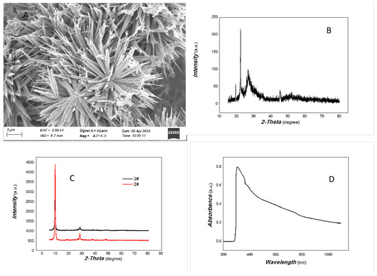
Figure 1.
A representative SEM image, XRD, and UV-Vis curve of MoVOx ((A) SEM; (B) 1#-XRD; (C) 2#,3#-XRD; (D) UV-Vis curve).
As can be seen in Figure 1A, the nanobelt has a very uniform morphology. The nanobelt is about 4–6 μm long. The width is approximately 40 nm. The uniform morphology of the MoVOx is excellent overall.
As shown in Figure 1B, the crystallinity of the MoVOx is not very good, while the noise level is bigger. However, some diffraction peaks can still be identified, such as those at 16.87°, 19.41°, 25.84°, 34.29°, 35.46°, 45.45°, 46.62°, 52.22°, and 56.44°, which are the peaks of the (110), (200), (210), (220), (310), (410), (404), (330), and (218) planes of MoO3 (PDF# 21-0569), respectively. The diffraction peaks at 26.85°, 27.52°, and 39.53° belong to the peaks of the (11-1), (011), and (002) planes of VO2 (PDF# 44-0252). As the amount of V doping increased, no significant diffraction peaks of VO2 were observed. This indicates that VO2 is not well crystallized or intercalated in the material. Otherwise, as shown in Figure 1C, 2θ at 9.39° is quite strong, indicating that the material growth is preferred along (100) planes of MoO3 (PDF# 21-0569). The diffraction angle is slightly reduced compared to the standard PDF (2θ at 9.69° (100)). It indicates that the V intercalation has increased the face spacing. Therefore, the resulting nanomaterial contains some MoO3 and VO2 components forming the MoVOx heterojunction.
As shown in Figure 1D, the optical absorption of the MoVOx was covered the entire visible spectrum and part of the near-infrared (NIR) region. Since the band gap width of MoO3 is approximately 2.8–3.85 eV, the absorption of the broad spectrum is likely due to V doping. Pepe and co-workers [37] have previously studied the nonlinear absorption and photoluminescence properties of Zn-, Fe-, Cu-, V-, and Ni-doped MoO3, examining the effects of these dopants on the band gap width. The results showed that doping significantly narrowed its bandgap, i.e., α-MoO3: 3.85 eV; Fe-doped α-MoO3: 3.46 eV; Cu-doped α-MoO3: 3.43 eV; Zn-doped α-MoO3: 3.34 eV; Ni-doped α-MoO3: 3.48 eV; V-doped α-MoO3: 3.67 eV. This study showed that the absorption edge of the V-doped MoO3 was located in the NIR region. This may be due to the introduction of intermediate states by V doping. Further support for the optoelectronic signals in the NIR is required later.
In the study of the interaction between light and matter, good optical absorption is crucial for detecting photoelectric signals. The detection of optoelectronic signals depends heavily on factors such as the width of the band gap, material defects, interface contacts, electrodes, and substrate. Gold is generally easy to characterize for this purpose, as it has a high work function and a low contact barrier. We first used gold electrodes to determine the photoelectric properties over a wide spectral range. Representative results are shown in Figure 2 and Figure 3.
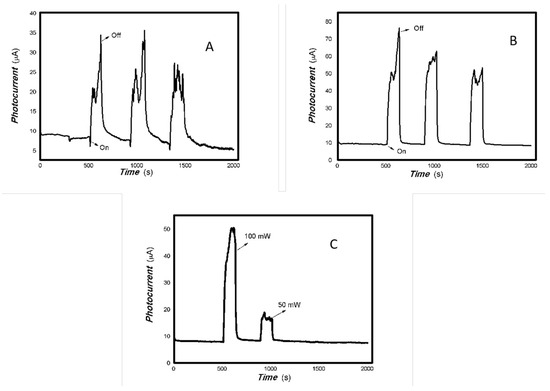
Figure 2.
The optoelectronic responses of MoVOx (1#) to the visible light ((A) 40 W visible light; (B) 100 mW 650 nm; (C) 100. 50, and 5 mW 650 nm) (using gold gap electrodes and PET film substrates, 1 V bias applied).
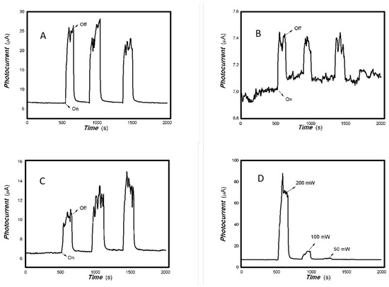
Figure 3.
The optoelectronic responses of MoVOx (1#) to 808, 980, and 1064 nm ((A) 200 mW 808 nm; (B) 20 mW 1064 nm; (C) 200 mW 980 nm; (D) 200, 100, 50, and 5 mW 980 nm) (using gold gap electrodes and PET film substrates, 1 V bias applied).
As shown in Figure 2 and Figure 3, the resulting MoVOx nanobelts can convert incident light signals into electrical signals. When visible light and certain wavelengths of near-infrared light hit the aggregated state of the nanobelts, the photons’ energy excites electrons, causing them to transition from the ground state to the excited state, and generate electron–hole pairs. An external bias then drives these photogenerated charges to move in a directed manner, forming a photocurrent. When the light is removed, the current gradually returns to its original state. This is the result of the interaction between light and matter producing non-equilibrium carriers. This is a typical reversible transition process from balanced carriers to unbalanced carriers. This clearly demonstrates that the carrier concentration in the material can be controlled by the light field. This indicates that the resulting nanocomposite is responsive to visible and near-infrared light stimuli. The nanocomposite is expected to have potential applications in multidisciplinary fields. Experiments also revealed that MoVOx (1#) nanobelts exhibited strong photocurrent signals in response to the light sources of 50 mW at 650 nm, 100 mW at 808 nm, 200 mW at 980 nm, and 20 mW at 1064 nm. This demonstrates that the MoVOx nanobelts can effectively utilize the visible light and NIR. This supports the results of UV-Vis curve of MoVOx (Figure 1D). Further confirmation was obtained that the resulting nanomaterial absorbs in the visible and near-infrared range. However, there was almost no response to the 5 mW light sources at 650 and 980 nm. This suggests that material defects trap all the photogenerated charges under low-incident power irradiation, making it difficult to extract the photocurrent signal. The representative results of the optoelectronic signals with an increasing V-doping content are shown in Figure 4 and Figure 5.
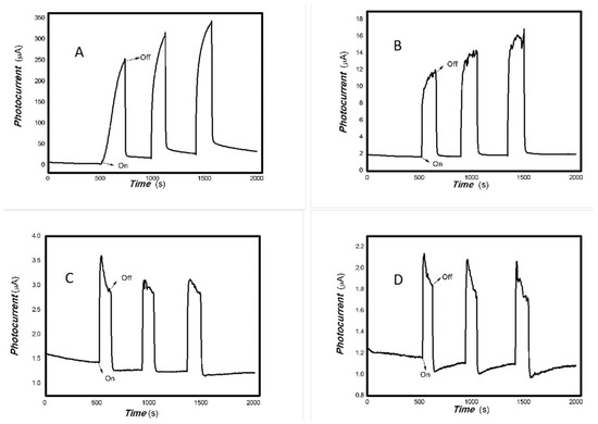
Figure 4.
The optoelectronic responses of MoVOx (2#) to 650, 808, 980, and 1064 nm ((A) 100 mW 650 nm; (B) 200 mW 808 nm; (C) 100 mW 980 nm; (D) 20 mW 1064 nm) (using gold gap electrodes and PET film substrates, 1 V bias applied).
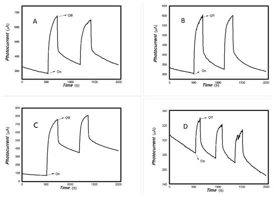
Figure 5.
The optoelectronic responses of MoVOx (3#) to 650, 808, 980, and 1064 nm ((A) 100 mW 650 nm; (B) 200 mW 808 nm; (C) 200 mW 980 nm; (D) 20 mW 1064 nm) (using gold gap electrodes and PET film substrates, 1 V bias applied).
As shown in Figure 4 and Figure 5, increasing the amount of V doping still allows for the photoelectric signals to be measured. However, the recovery time is relatively long and the baseline current is less stable. Regarding the nanocomposite itself, the VO2 has a low degree of crystallization (Figure 1B), with almost no noticeable effect from increased V addition (Figure 1C). Low crystallinity means an increased disorder degree in the material. High disorder leads to increased non-radiative energy consumption and a large photothermal effect. The slow response and recovery in Figure 4 and Figure 5 also illustrate these issues. In the fields of luminescence, solar cells and photodetectors, decreasing non-radiative energy consumption requires control of the material’s microstructure. This photothermal effect will also be utilized in other interdisciplinary fields. A low degree of crystallization increases the likelihood of electron–electron and electron–phonon scattering, slowing down charge transport.
The study of light matter interactions involves many photophysical properties and physical mechanisms, as well as multidisciplinary applications. Some ideas from the fields of photodetectors and solar cells provide excellent inspiration for multidisciplinary applications [76,77,78]. Important performance parameters, such as open-circuit voltage, short-circuit current, responsivity (R), external quantum efficiency (EQE), and detectivity (D) accurately reflect the key performance of solar cells and photodetectors. However, our research does not focus on these devices or related materials. Our focus is on interdisciplinary aspects and complementary content based on qualitative and semi-quantitative characterization. To this end, we have summarized key data from Figure 2, Figure 3, Figure 4 and Figure 5 and in Table 1 for easier analysis and discussion.

Table 1.
The comparative photocurrent signals of 1#, 2#, 3#-MoVOx nanobelt aggregation states using Au gap electrodes and PET film to some representative light sources (1 V bias applied).
As shown in Table 1, the switching ratio initially increases and then decreases as the V doping concentration rises for 650 nm, 808 nm, and 980 nm light sources. Meanwhile, the response and recovery speeds slow down accordingly. This trend is also generally observed for other light sources, albeit with greater fluctuations. This indicates that, as the amount of V added increases, the degree of disorder, the number of defects and the amount of non-radiative energy consumption increase, leading to more scattering opportunities and causing greater fluctuations. This includes both the photoelectric and photothermal effects. The photothermal effect is inevitable.
Based on the results shown in Figure 2, Figure 3, Figure 4 and Figure 5, it can be confirmed that the synthesized MoVOx nanobelts exhibit good optoelectronic signals in the broadband spectral range when used with gold gap electrodes. This is likely due to V-doping creating intermediate states, thereby increasing the potential for photoexcitation and electron transformation. In addition to the materials and their microstructures themselves, the electrodes and substrates also play an important role in acquiring optoelectronic signals. The acquisition of optoelectronic signals is the result of various factors combined. Untreated paper is known to contain a large number of defects, particularly O groups. These groups tend to trap photogenerated electrons, which hinders the acquisition of optoelectronic signals when using untreated paper as a substrate. Conversely, graphite electrodes with pencil drawings were among the most cost-effective in the study. These electrodes were composed of 84% graphite and 16% clay. These carbon electrodes themselves can be regarded as composites, and their defects cannot be ignored. The use of these carbon electrodes naturally traps some of the photogenerated carriers, which can degrade the photoelectric signal. Another important factor in driving the carrier transfer is the bias applied. Applying a suitable external bias voltage drives the directional flow of carriers and prevents photogenerated carrier recombination. To suppress photogenerated carrier recombination, the material itself must have a strong built-in electric field to drive charge movement. Taking these factors into account, the MoVOx nanobelts were chosen to investigate the effect of bias voltage on photogenerated current using A4 printing paper as substrates and the graphite electrodes with 6B pencil drawings. Representative results are shown in Figure 6, Figure 7, Figure 8, Figure 9, Figure 10, Figure 11 and Figure 12.
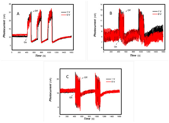
Figure 6.
The effect of the bias voltage on the photogenerated current for the MoVOx (1#) to 808, 980, and 1064 nm ((A) 200 mW 808 nm; (B) 100 mW 980 nm; (C) 20 mW 1064 nm) (Red line: 0 V bias; Black line: 1 V bias) (using A4 printing paper as substrates and the graphite electrodes with 6B pencil drawings).
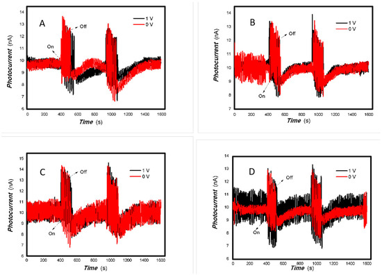
Figure 7.
The effect of the bias voltage on the photogenerated current for the MoVOx (1#) to 405, 532, 650, and 780 nm ((A) 50 mW 405 nm; (B) 50 mW 532 nm; (C) 50 mW 650 nm; (D) 50 mW 780 nm) (Red line: 0 V bias; Black line: 1 V bias) (using A4 printing paper as substrates and the graphite electrodes with 6B pencil drawings).
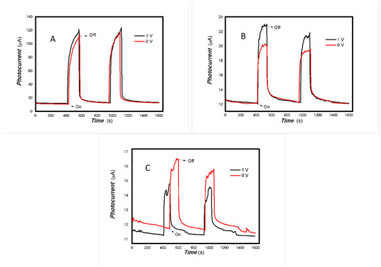
Figure 8.
The effect of the bias voltage on the photogenerated current for the MoVOx (3#) to 808, 980, and 1064 nm ((A) 200 mW 808 nm; (B) 100 mW 980 nm; (C) 20 mW 1064 nm) (Red line: 0 V bias; Black line: 1 V bias) (using A4 printing paper as substrates and the graphite electrodes with 6B pencil drawings).
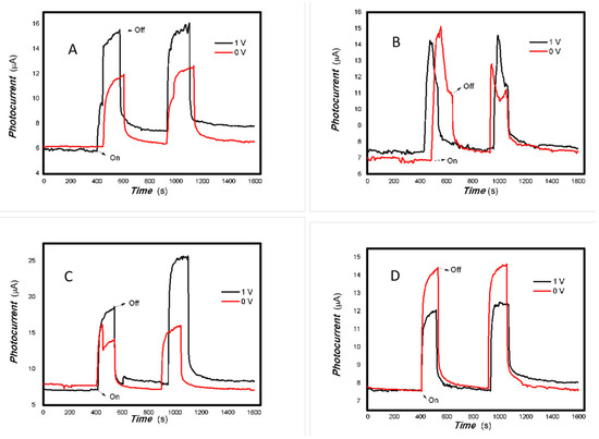
Figure 9.
The effect of the bias voltage on the photogenerated current for the MoVOx (3#) to 405, 532, 650, and 780 nm ((A) 50 mW 405 nm; (B) 50 mW 532 nm; (C) 50 mW 650 nm; (D) 50 mW 780 nm) (Red line: 0 V bias; Black line: 1 V bias) (using A4 printing paper as substrates and the graphite electrodes with 6B pencil drawings).
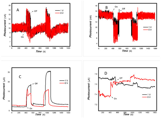
Figure 10.
The effect of the bias voltage and power of typical light sources on the photogenerated current for the MoVOx (1, 3#) to 650 nm (Red line: 0 V bias; Black line: 1 V bias) ((A) 1# to 50 mW 650; (B) 1# to 5 mW 650 nm; (C) 3# to 50 mW 650; (D) 3# to 5 mW 650 nm) (using A4 printing paper as substrates and the graphite electrodes with 6B pencil drawings).
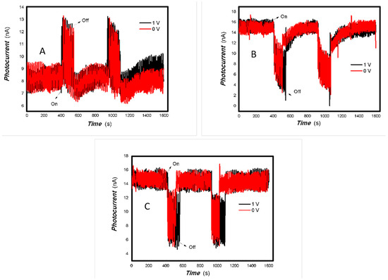
Figure 11.
The effect of the bias voltage and power of typical light sources on the photogenerated current for the MoVOx (1#) to 980 nm (Red line: 0 V bias; Black line: 1 V bias) ((A) 100 mW; (B) 50 mW; (C) 5 mW) (using A4 printing paper as substrates and the graphite electrodes with 6B pencil drawings).
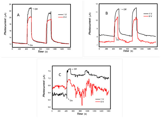
Figure 12.
The effect of the bias voltage and power of typical light sources on the photogenerated current for the MoVOx (3#) to 980 nm (Red line: 0 V bias; Black line: 1 V bias) ((A) 100 mW; (B) 50 mW; (C) 5 mW) (using A4 printing paper as substrates and the graphite electrodes with 6B pencil drawings).
As can be seen in Figure 6, Figure 7, Figure 8, Figure 9, Figure 10, Figure 11 and Figure 12, a good photoelectric signal was still determined even when zero bias was applied and the graphite electrodes with 6B pencil drawings on A4 printing paper were used. This indicates that the MoVOx nanobelts can produce a strong intrinsic electric field to promote photogenerated carrier transport, enabling self-powering. Self-powered devices are an important area of research due to their low energy consumption [79,80,81,82]. Similarly, self-driven nanomaterials also play a significant role in preventing the recombination of photogenerated charges. In most cases, the bias applied in this study was found to have little effect. Increasing the bias voltage increases the photogenerated current when the material is excited by light of certain wavelengths. This demonstrates that interfaces exist within the mixed oxides prepared by the one-pot method. Charge transfer between these interfaces generates a built-in electric field. The built-in electric field created by the MoVOx nanobelts is strong enough to facilitate the transport of photogenerated charges, and inhibit their recombination. Increasing the V-doping content significantly increases the base current from nA to μA. This is mainly due to the unfilled d electrons of the V element. This suggests that V doping can enhance the conductivity of the mixed oxide. This improves the transport of photogenerated carriers. However, as shown in Figure 6, a large fluctuation in the photocurrent of the MoVOx nanobelts was observed when a 20 mW, 1064 nm light source was used. This may be due to electron-electron and electron-phonon scattering affecting charge transport. Therefore, controlling the microstructure of materials is important in terms of suppressing the recombination of photogenerated carriers and reducing non-radiative energy consumption. The presence of an internal electric field can suppress photogenerated charge recombination, which is useful for the material itself.
Additionally, Figure 10, Figure 11 and Figure 12 show an interesting phenomenon: a transition from positive to negative photoconductivity in the low V-doping sample as the power of typical light sources decreased. This phenomenon was not observed in the high V doping mixed oxide sample. This reflects the result of an imbalance between the concentration of material defects and the concentration of photogenerated electrons. As the power of the light sources was reduced further, the concentration of photogenerated electrons decreased too. When the concentration of photogenerated electrons is lower than the concentration of material defects, all the photogenerated electrons are trapped by the material defects. The net increase in photocurrent is negative. This indicates negative conductivity. Heavily V-doped MoO3 resulted in a high VO2 content in the heterojunction. Since the valence state of V varies between +2 and +5, VO2 contains many oxygen vacancies, which have an electron-donating effect. This electron-rich effect of VO2 can passivate the material defects, resulting in a positive net increase in current. This response is known as defect-assisted photoconductive behavior. Additionally, highly V-doped MoO3 exhibits plasmonic effects that contribute to the interfacial charge transfer. In our previous publication [83], we introduced the phenomenon of the transition from negative to positive photocurrent response by passivating the grain boundary defects of the nanocomposite with metal nanomaterials. Consequently, the impact of material defects and interfaces on the acquisition of optoelectronic properties was substantial. The modulation of material defects for different applications is an ongoing process.
For ease of comparison, the key data in Figure 6, Figure 7, Figure 8 and Figure 9 are summarized in Table 2.
Table 2.
The comparative photocurrent signals of 1#, 3#-MoVOx nanobelt aggregation states using carbon electrodes with 6B pencil drawings and A4 paper as a substrate to some representative light sources (0 V bias applied). * Negative photoconductivity.
As shown in Table 2, as the V doping concentration increases, the switching ratio increases, while the response and recovery speeds slow down accordingly. This indicates an increase in defects, which in turn exacerbates scattering and affects the response speed. Under light irradiation of 5 mW at 650 nm (it is shown in Figure 10), and 5, 50 mW at 980 nm (it is shown in Figure 11), 1#-MoVOx nanobelts exhibit a negative photoconductive effect. This is due to an imbalance between the defect concentration and the photogenerated carrier concentration. All photogenerated electrons are captured by defects, leading to a decrease in the photocurrent. On the other hand, it also shows that even when using carbon electrodes and paper substrates, it is still possible to obtain broad-spectrum photocurrent signals. Defects originate not only from the MoVOx nanobelt itself, but also from the carbon electrodes with 6B pencil drawings and paper substrate. Despite the presence of so many defects, it is still significant that photogenerated carriers can still be extracted. From the perspectives of cost and multidisciplinary research, the findings are highly valuable.
Since it is still possible to achieve better photoelectric signal extraction at zero bias using graphite electrodes with 6B pencil drawings, the effect of bias on the photoelectric signal was examined again using gold electrodes due to Au’s low barrier. Representative results are shown in Figure 13, Figure 14, Figure 15, Figure 16, Figure 17, Figure 18, Figure 19, Figure 20, Figure 21, Figure 22, Figure 23, Figure 24, Figure 25 and Figure 26. Since the resulting oxide nanobelts have been stored at room temperature for over 2 years, these research results also reflect the photophysical stability of the nanomaterials.
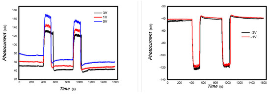
Figure 13.
The effects of bias on the optoelectronic signal to 200 mW 808 nm light source for the 1#-MoVOx (using Au gap electrodes on PET film).
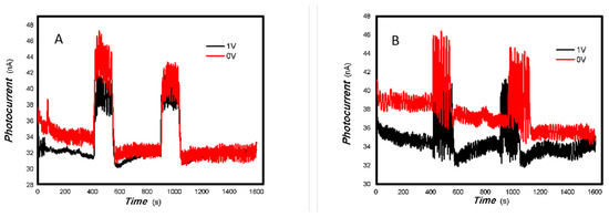
Figure 14.
The effects of bias on the optoelectronic signal to the 980 and 1064 nm light sources for the 1#-MoVOx ((A) 980 nm (100 mW); (B) 1064 nm (20 mW)) (using Au gap electrodes on PET film).
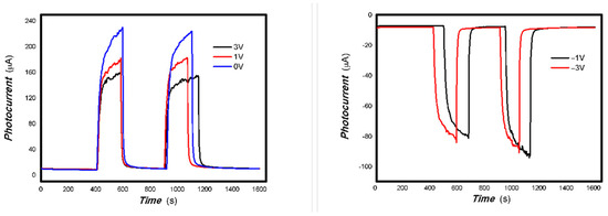
Figure 15.
The effects of bias on the optoelectronic signal to 200 mW 808 nm light source for the 2#-MoVOx (using Au gap electrodes on PET film).
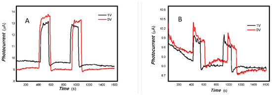
Figure 16.
The effects of bias on the optoelectronic signal to the 980 and 1064 nm light sources for the 2#-MoVOx ((A) 980 nm (100 mW); (B) 1064 nm (20 mW)) (using Au gap electrodes on PET film).
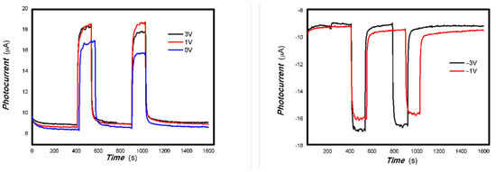
Figure 17.
The effects of bias on the optoelectronic signal to the 980 nm light source for the 3#-MoVOx (using Au gap electrodes on PET film).
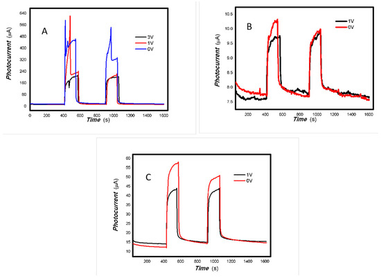
Figure 18.
The effects of bias on the optoelectronic signal to the representative light sources for the 3#-MoVOx ((A) 808 nm (200 mW); (B) 1064 nm (20 mW); (C) 650 nm (50 mW)) (using Au gap electrodes on PET film).
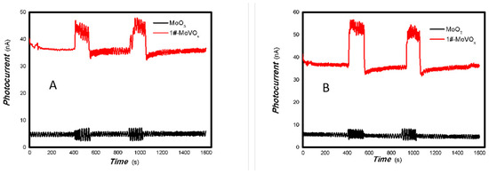
Figure 19.
The effects of V doping on the optoelectronic signal of 1#-MoVOx ((A) 405 nm (50 mW); (B) 650 nm (50 mW)) (using Au gap electrodes on PET film).
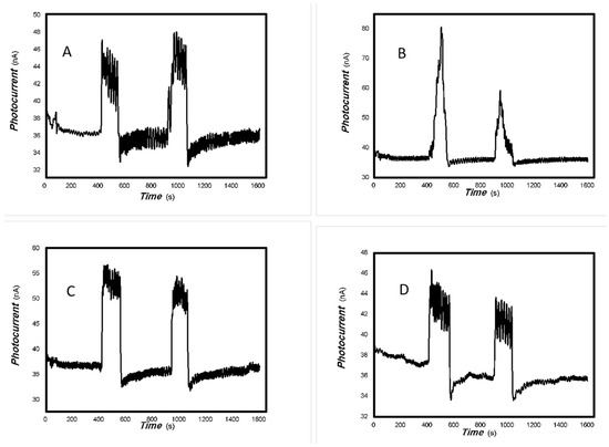
Figure 20.
The comparative photocurrent signals of 1#-MoVOx to the light source with different wavelengths ((A) 50 mW 405 nm; (B) 50 mW 532 nm; (C) 50 mW 650 50 mW; (D) 50 mW 780 nm) (using Au gap electrodes on PET film).
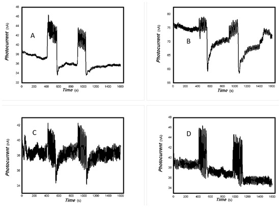
Figure 21.
The comparative photocurrents signals of 1#-MoVOx to the light source with different wavelengths ((A) 780 nm (50 mW); (B) 808 nm (50 mW); (C) 980 nm (50 mW); (D) 1064 nm (20 mW)) (using Au gap electrodes on PET film).
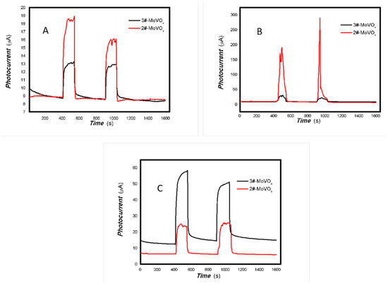
Figure 22.
The comparative photocurrents signals of 2#,3#-MoVOx to the light source with different wavelengths ((A) 405 nm (50 mW); (B) 532 nm (50 mW); (C) 650 nm (50 mW)) (using Au gap electrodes on PET film).
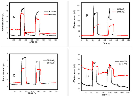
Figure 23.
The comparative photocurrents signals of 2#,3#-MoVOx to the light source with different wavelength ((A) 780 nm (50 mW); (B) 808 nm (200 mW); (C) 980 nm (100 mW); (D) 1064 nm (20 mW)) (using Au gap electrodes on PET film).
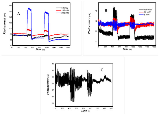
Figure 24.
The dependence of the photocurrent signals of 1#-MoVOx on the power of incident light sources ((A) 808 nm; (B) 980 nm; (C) 5 mW 980 nm) (using Au gap electrodes on PET film).
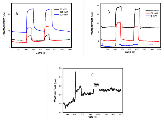
Figure 25.
The dependence of the photocurrent signals of 2#-MoVOx on the power of incident light sources ((A) 808 nm; (B) 980 nm; (C) 5 mW 980 nm) (using Au gap electrodes on PET film).
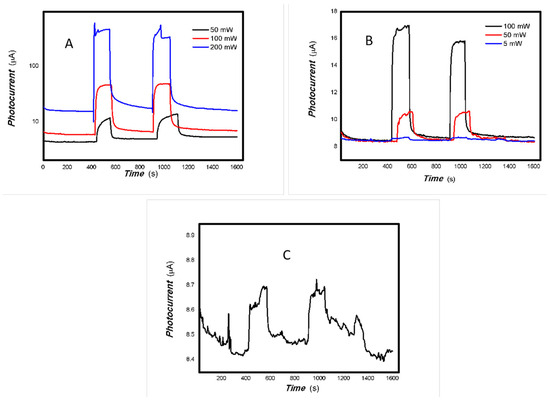
Figure 26.
The dependence of the photocurrent signals of 3#-MoVOx on the power of incident light sources ((A) 808 nm; (B) 980 nm; (C) 5 mW 980 nm) (using Au gap electrodes on PET film).
The effect of bias on the optoelectronic signal was examined by selecting several representative light sources first. These results are shown in Figure 13, Figure 14, Figure 15, Figure 16, Figure 17 and Figure 18.
Figure 13 shows that the bias has a little effect on the optoelectronic signal to 200 mW 808 nm light source for the 1#-MoVOx.
Figure 14 shows that the applying a bias voltage slightly reduces the photoelectric signal for the 1#-MoVOx sample with 980 nm and 20 mW 1064 nm light sources. This trend of decrease is more obvious for the 2#-MoVOx sample. These results are shown in Figure 15 and Figure 16. This is primarily due to the built-in electric field being in the opposite direction to the applied bias voltage, which counteracts part of the driving force for charge transfer.
Figure 17 and Figure 18 demonstrate that applying a bias voltage significantly increases the transfer of photogenerated charge. This indicates differences in the strength of the built-in electric field of various V-doped nanocomposites, reflecting the differing effects of applying different bias voltages to photogenerated electrical signals.
In order to compare the doping effect of different V, representative light sources were selected and examined. This is shown in Figure 19.
Figure 19 shows that low V doping improves both the photoelectric signal and the base current. V doping can improve the conductivity of the material. However, the 50 mW 405 and 650 nm light sources triggered large fluctuations in the base current for the MoO3 reference sample only. This suggests that radiation from these light sources increases the likelihood of collisions between electrons and material defects, resulting in significant fluctuations in the base current.
The above experimental investigations illustrate that the prepared mixed oxides themselves have a built-in electric field that can drive the directional movement of photogenerated charges to form photocurrents. The effect of zero bias applied on different wavelengths of light is shown in Figure 20 and Figure 21.
Figure 20 and Figure 21 demonstrate that the 1#-MoVOx nanobelts still exhibited excellent photocurrent extraction capabilities when exposed to light sources of 50 mW at 405, 650, 780, and 980 nm, as well as 20 mW at 1064 nm, with a bias of 0 V applied.
It was found that increasing V doping improves the electrical conductivity of the material. The baseline current changes from nA to μA. To facilitate the comparison of the effect of increasing V doping on the photoelectric signals, the photoelectric signals of the 2#, 3# nanocomposite samples were compared in the same figure. The results are shown in Figure 22 and Figure 23.
Figure 22 and Figure 23 demonstrate that the photoelectric signal in the near-infrared (NIR) region (780, 808, 980 and 1064 nm) increases significantly with V doping. Therefore, V doping greatly increases the red shift of the material.
For ease of comparison and analysis, some of the key data from the above figure are summarized in Table 3.
Table 3.
The comparative photocurrent signals of 1#, 2#, 3#-MoVOx nanobelt aggregation states using Au gap electrodes and PET film to some representative light sources (0 V bias applied).
As shown in Table 3, the general trend is that the photoconductivity ratio first increases and then decreases as the V doping concentration increases. The response and recovery times are also prolonged. There are also some fluctuations. This is primarily due to the numerous defects present in the mixed oxides. Defect-induced scattering reduces charge transport, leading to significant baseline and photocurrent fluctuations. A comparison of Table 2 and Table 3 shows that the resulting material using Au electrodes and a PET film substrate did not exhibit a negative photoconductive effect. This indicates that the defects in the carbon electrode with 6B pencil drawings and paper substrate played a significant role for the acquisition of optoelectronic signals and photoconductive behaviors. Light scattering caused by defects plays an important role in the fluctuation of photocurrent.
The representative results of their photoelectric signals dependent on the incident light power are shown in Figure 24, Figure 25 and Figure 26.
As shown in Figure 24, Figure 25 and Figure 26, the photoelectric signal clearly depends on the incident light power. A good photoelectric signal is still obtained with increased V doping (samples 2# and 3#) for a 5 mW, 980 nm light source. This is demonstrated in Figure 25 and Figure 26. However, there is significant fluctuation at a low V doping amount for a 5 mW, 980 nm light source. This is shown in Figure 24. This is primarily due to the fact that mixed oxides with low V doping contain more defects that can easily capture photogenerated electrons, thereby increasing the likelihood of electron-electron and electron-defect collisions. This affects charge transport and leads to large photocurrent fluctuations. A comparison of Figure 22 and Figure 23 shows that sample 2# has higher near-infrared (NIR) photoelectric sensitivity. The improvement in near-infrared photoconductivity is mainly due to the appropriate doping concentration of V element. According to the reference [84], the band gap of VO2 is approximately 1.17 eV, this is the primary reason for the enhanced near-infrared photoelectric sensitivity. However, other factors, including changes in the valence state, plasma characteristics and the high proportion of amorphous material, also affect its photophysical properties and physical mechanisms. These factors work together to promote the extraction of photo-generated charges from the material and bring about different physical effects. The one-pot preparation of nanocomposites that exhibit photogenerated charge extraction properties in the near-infrared spectrum has been demonstrated to be a simple and feasible process. Suppressing photogenerated carrier recombination and improving charge extraction properties is important for applications in multidisciplinary fields [85]. As electron–hole recombination has been a key bottleneck in these fields for several decades, this study focused on a different nanocomposite system to improve the extraction of photogenerated charges across the broadband spectrum. This provides an important reference for these fields.
3. Materials and Methods
3.1. Raw Materials
The following materials were used in this study: sodium molybdate dihydrate (analytical reagent, AR), Tianjin Fengchuan Chemical Reagent Co. (Tianjin, China); ammonium metavanadate (NH4VO3) (AR), Tianjin Bodi Chemical Co (Tianjin, China); and hydrochloric acid (AR), Hongteng Weiye New Material Co., Ltd. (Yantai, China).
3.2. Synthesis of MoVOx Mixed Oxide with One Pot
The dilute hydrochloric acid and the synthesis of MoVOx was similar to that of MoO3 in reference [74]. First, 1 g of sodium molybdate was added to 1#, 2#, 3# hydrothermal kettle, and then 40 mL of dilute hydrochloric acid, 20 mL of H2O, and 0.2 g, 0.5 g, 0.8 g ammonium metavanadate were added, and stirred for about 10 min. The hydrothermal reaction was maintained at 170 °C for 6 h. The resulting products are labeled 1#, 2#, 3#-MoVOx. The synthesis process of the MoVOx is as follows (it is shown in Scheme 1).
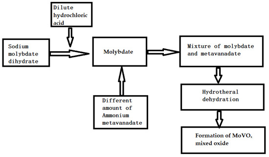
Scheme 1.
The synthesis process of the MoVOx.
3.3. Characterization with SEM, UV-Vis-NIR Spectrum, and XRD
The characterizations by scanning electron microscope (SEM), UV-VIS-NIR spectrophotometer (UV-Vis-NIR) and X-ray powder diffraction (XRD) were similar to the reference [74,75,83]. The instruments used were a ZEISS Gemini SEM300 (Oberkochen, Germany), TU-1810 spectrophotometer (Beijing Puxi General Instrument Co., Ltd., Beijing, China), and XRD-7000 from SHIMADZU (Shimadzu, Kyoto, Japan).
3.4. Measurement of the Optoelectronic Signal of MoVOx Mixed Oxide in the Wide Spectral Range
The MoVOx mixed oxide suspension was cast on the Au gap electrodes on a flexible polyethylene terephthalate (PET) film. For the photodetector structure of the photoconductor type, the structure of the electrodes is shown in Scheme 2. The determination of the optoelectronic response to the weak visible light (40 W) or 405, 532, 650 nm (100, 50, and 5 mW) and 780, 808, 980, and 1064 nm NIR (10, 40, 50, 100, and 200 mW) was similar to that in reference [74,75,83]. Another electrodes was used 6B pencil drawings and A4 printing paper as a substrate in this study. The bias applied was 0 and 1 V.
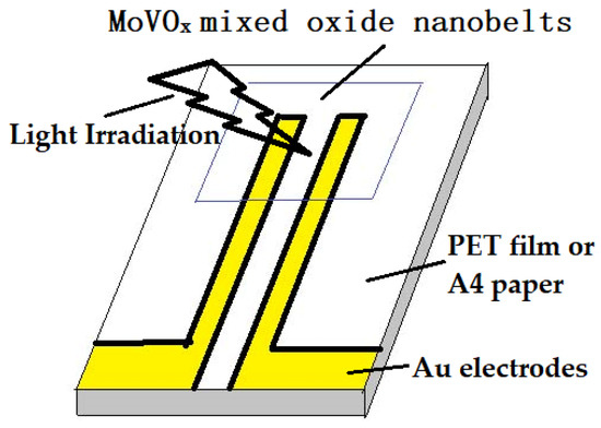
Scheme 2.
The structure of the electrodes used in this study.
4. Conclusions
In short, the MoVOx mixed oxide nanobelt was synthesized using the one-pot hydrothermal method. Good photoelectric signals were still measured within the broadband light response range, even with zero bias applied, and using graphite electrodes with 6B pencil drawings and Au electrodes. This demonstrates that the MoVOx mixed oxide presents a strong built-in electric field that promotes the photogenerated carrier transport, which can be self-powered. Doping with V significantly improved the NIR photoelectric sensitivity of the nanocomposites, and brought about different physical effects. This inexpensive, simple method can be used to obtain metal oxide nanocomposites that exhibit a photocurrent response over a wide spectral range. It is also expected to be suitable for bandgap narrowing in other wide-bandgap oxide material systems. These results are probably due to the introduction of intermediate states through V doping or intercalation. This study also provides an effective way to suppress the recombination of photogenerated carriers by controlling the microstructure of the nanocomposite and forming a strong built-in electric field.
Author Contributions
Conceptualization, methodology, investigation, writing—original draft preparation, writing—review and editing, funding acquisition, resources, X.M.; investigation, X.M., X.Z., M.G., R.H. and Y.W.; resources, G.L.; all authors analyzed the data; all authors discussed the results of the paper. All authors have read and agreed to the published version of the manuscript.
Funding
This project was supported by the Natural Science Foundation of Shandong Province (project no. ZR2013EMM008).
Institutional Review Board Statement
Not applicable.
Informed Consent Statement
Not applicable.
Data Availability Statement
The data presented in this study are available on request from the corresponding author. The data are not publicly available due to privacy.
Acknowledgments
Thanks to You Wang and Guang Li of Zhejiang University for the fabrication of several electrodes, and for checking the English of the paper for many times. The SEM was performed by Jie Su at the Structural Composition Testing Center, School of Chemistry and Chemical Engineering, Shandong University. Some students, such as Guiting Dou, performed part of the experiments.
Conflicts of Interest
The authors declare no conflicts of interest.
References
- Soundharaya, J.; Raksha, A.; Rajni, K.S.; Senthilkumar, N.; Eswaramoorthy, N.; Raguram, T. Construction of Cu-doped α-MoO3 nanostructures and their application as counter electrode in dye-sensitized solar cells. Mater. Lett. 2024, 359, 135773. [Google Scholar] [CrossRef]
- Milani, E.A.; Piralaee, M.; Raeyani, D.; Asgari, A. High-performance semi-transparent organic solar cells for window applications using MoO3/Ag/MoO3 transparent anodes. Sol. Energy Mater. Sol. Cells 2024, 276, 113066. [Google Scholar] [CrossRef]
- Şakar, B.C.; Yıldırım, F.; Aydoğan, Ş. Highly stable, self-powered UV-Vis-NIR broadband isotype photodetector based on Ti-doped amorphous MoO3. Sens. Actuators A Phys. 2024, 370, 115216. [Google Scholar] [CrossRef]
- Yadav, A.; Khan, A.; Kumar, A.; Khanuja, M.; Pathi, P.; Gupta, G. Highly responsive MoS2/MoO3 heterojunction based broadband photodetector. Opt. Mater. 2024, 157, 116227. [Google Scholar] [CrossRef]
- Subramaniyan, S.; Govindasamy, M.; Sakkarapani, S.; Kuo, C. Exploration of CeO2 decorated on MoO3 as a potential electrode for high performance hybrid supercapacitors. J. Alloys Compd. 2025, 1013, 178518. [Google Scholar] [CrossRef]
- Modi, K.H.; Pataniya, P.M.; Bhadu, G.; Sumesh, C.K. Self-supported SnS/MoO3 electrocatalyst for supercapacitor and hydrogen evolution reaction. J. Energy Storage 2024, 99, 113475. [Google Scholar] [CrossRef]
- Dabir, M.P.; Masoudpanah, S.M.; Mamizadeh, M. Ultrathin needle-like NiMoO4/MoO3 heterostructure for supercapacitor and overall water splitting applications. J. Energy Storage 2024, 82, 110542. [Google Scholar] [CrossRef]
- Sun, Y.; Li, T.; Liu, X.; Han, Y.; Liu, Y.; Zada, A.; Deng, W.; Yuan, Z.; Dang, A. Modulating oxygen vacancies in MXene/MoO3-x smart fiber by defect engineering for ultrahigh volumetric energy density supercapacitors and wearable SERS sensors. Chem. Eng. J. 2024, 494, 152911. [Google Scholar] [CrossRef]
- Shaheen, N.; Zulfiqar, S.; El Sayed, M.E.; Samir, A.; Shahid, M.; Warsi, M.F.; Cochran, E.W. Evaluation of energy storage mechanism and development of nanoarchitecture in 1D WS2/MoO3/MXene composite for supercapacitor applications. J. Alloys Compd. 2025, 1010, 178072. [Google Scholar] [CrossRef]
- Song, Y.Z.; Liu, Z.X.; Huang, Y.A. Synthesis of MnMoO4/α-MoO3 composite materials for supercapacitor. Inorg. Chem. Commun. 2024, 170, 113481. [Google Scholar] [CrossRef]
- Yue, X.; Zhang, J.; Chen, D.; Xu, X.; Wu, H.; Zhou, Y.; Liang, Z. Multifunctional α-MoO3 Nanobelt Interlayer with the Capacity Compensation Effect for High-Energy Lithium-Sulfur Batteries. ACS Appl. Mater. Interfaces 2023, 15, 13064–13072. [Google Scholar] [CrossRef]
- Wei, K.; Qiu, J.; Zhao, Y.; Ma, S.; Wei, Y.; Li, H.; Zeng, C.; Cui, Y. Tunable oxygen vacancies in MoO3 lattice with improved electrochemical performance for Li-ion battery thin film cathode. Ceram. Int. 2023, 49, 21729–21736. [Google Scholar] [CrossRef]
- Wu, Y.; Liu, W.; Zhang, Z.; Zheng, Y.; Fu, X.; Lu, J.; Cheng, S.; Su, J.; Gao, Y. Defect-Rich MoO3 Nanobelts for ultrafast and wide-temperature proton battery. Energy Storage Mater. 2023, 61, 102849. [Google Scholar] [CrossRef]
- Qin, J.; Sun, B.; Mao, S.; Yang, Y.; Liu, M.; Rao, Z.; Ke, C.; Zhao, Y. Improved resistive switching performance and mechanism analysis of MoO3 nanorods based memristors. Mater. Today Commun. 2023, 36, 106770. [Google Scholar] [CrossRef]
- Ma, K.; Kim, S.; Kim, H.Y.; Seo, I.; Han, S.H.; Shin, S.; Jang, H.S.; Kim, D.H. Mechanical and electrical properties of α-MoO3 belts under strain for flexible electronics applications. Appl. Surf. Sci. 2025, 681, 161512. [Google Scholar] [CrossRef]
- Li, J.; Wang, N.; Yang, X.; Li, J.; Xiong, S.; Fu, H.; An, X. Conductometric triethylamine sensor based on Pd nanoparticles modified Fe doped MoO3 porous nanobelts. Sens. Actuators B Chem. 2025, 137289. [Google Scholar] [CrossRef]
- Zhang, S.; Wang, Q.; Song, P. Design of narrow bandgap Fe2O3/MoO3 heterostructure for boosting triethylamine sensing performance. ChemPhysMater 2024, 3, 284–292. [Google Scholar] [CrossRef]
- Habashyani, S.; Budak, S.M.H.F.; Kasapoglu, A.E.; Çoban, O.; Gür, E. Electrochromic properties of undoped and Ti-doped MoO3 converted from vertical nanowall MoS2 thin films. Electrochim. Acta 2024, 498, 144638. [Google Scholar] [CrossRef]
- Vinay Kumar, E.; Harini, R.; Bhuvaneshwari, H.S.; Sushma, P.M.; Sushmitha, D.S.; Kumara Swamy, B.E.; Anitha, G.; Nagaraju, G. Facile green synthesis of Zn doped MoO3 nanoparticles and its photocatalytic and photoluminescence studies. J. Mol. Struct. 2024, 1312, 138494. [Google Scholar] [CrossRef]
- Tian, R.; Ding, Y.; Wang, Q.; Song, P. Advanced triethylamine sensor utilizing 3D microspheres of La-doped MoO3: Performance enhancement and mechanism insights. Sens. Actuators B. Chem. 2024, 412, 135817. [Google Scholar] [CrossRef]
- Khanlary, M.R.; Parhizkari, M.; Heydari, N. Structural and optical properties of 1T-MoS2/MoO3 thin films prepared by spray pyrolysis method. Phys. B Condens. Matter 2024, 680, 415837. [Google Scholar] [CrossRef]
- Nasser, R.; Zhou, H.; Li, F.; Elhouichet, H.; Song, J. Heterostructured MoO3@CoWO4 nanobelts towards high electrochemical performances via oxygen vacancies generation. J. Colloid Interface Sci. 2024, 654, 805–818. [Google Scholar] [CrossRef] [PubMed]
- Roy, D.; Das, B.K.; Riaz, S.N.; Das, D.; Sarkar, S.; Chattopadhyay, K.K. Oxygen Vacancy-Induced Band Engineering and Metal Unsaturation in MoS2-MoO3 with Spillover-Based Confined Catalysis. ACS Appl. Energy Mater. 2023, 6, 4892–4908. [Google Scholar] [CrossRef]
- Jansi, R.; Revathy, M.S.; Vinoth, S.; Kumar, A.; Isaac, R.S.R.; Deepa, N. Abdullah Al-Enizi, Mohd Ubaidullah, Bidhan Pandit, Mohd Shahazad, Manish Gupta, Improvement in ammonia gas sensing properties of La doped MoO3 thin films fabricated by nebulizer spray pyrolysis method. Opt. Mater. 2023, 145, 114464. [Google Scholar] [CrossRef]
- Naveen, M.V.; Krishnamurthy, G.; Yuvaraj, T.C.M.; Harini, R.; Manjuraj, T.; Anitha; Nagaraju, G. Enhanced photocatalytic applications of Ce-doped MoO3 nanoparticles synthesized via combustion process using Calophyllum seed powder. J. Mol. Struct. 2025, 1328, 141125. [Google Scholar] [CrossRef]
- Dumrongrojthanath, P.; Phuruangrat, A.; Thipkonglas, S.; Kuntalue, B.; Thongtem, S.; Thongtem, T. Synthesis and characterization of Ce-doped MoO3 nanobelts for using as visible-light-driven photocatalysts. Superlattices Microstruct. 2018, 120, 241–249. [Google Scholar] [CrossRef]
- Liu, Z.; Jin, Y.; Teng, F.; Hua, X.; Chen, M. An efficient Ce-doped MoO3 catalyst and its photo-thermal catalytic synergetic degradation performance for dye pollutant. Catal. Commun. 2015, 66, 42–45. [Google Scholar] [CrossRef]
- Tutel, Y.; Durukan, M.B.; Hacioglu, S.O.; Baskose, U.C.; Toppare, L.; Unalan, H.E. Cobalt-doped MoO3 thin films and dual-band electrochromic devices with excellent cyclic stability. Appl. Mater. Today 2023, 35, 101924. [Google Scholar] [CrossRef]
- Khalid, N.R.; Hasnain, M.; Ali, F.; Siddique, S.; Iqbal, T.; Rafique, M.; Imran, M.; Assiri, M.A. Green synthesized, photocatalytic Co-doped MoO3 nanospheres for wastewater treatment. Ceram. Int. 2024, 50, 9640–9649. [Google Scholar] [CrossRef]
- Benameur, N.; Chakhoum, M.A.; Boukhachem, A.; Dahamni, M.A.; Ghamnia, M.; Hacini, N.; Pireaux, J.-P.; Houssiau, L.; Ziouche, A. Investigation of some physical properties of pure and Co-doped MoO3 synthesized on glass substrates by the spray pyrolysis method. J. Electron Spectrosc. Relat. Phenom. 2019, 234, 71–79. [Google Scholar] [CrossRef]
- Yue, L.; Ma, L.; Zhao, Z.; Gong, F.; Yang, X.; Zhang, Y. Synthesis of mesoporous cobalt-doped MoO3 nanoribbons for highly selective detection of triethylamine. Mater. Lett. 2024, 377, 137552. [Google Scholar] [CrossRef]
- Gomathi, K.; Padmanathan, S.; Ali, A.M.; Rajamanickam, A.T. Construction of Ni doped MoO3 nanostructures and their application as counter electrode in dye-sensitized solar cells. Inorg. Chem. Commun. 2022, 135, 109079. [Google Scholar] [CrossRef]
- Jiang, W.; Meng, L.; Zhang, S.; Chuai, X.; Zhou, Z.; Hu, C.; Sun, P.; Liu, F.; Yan, X.; Lu, G. Design of highly sensitive and selective xylene gas sensor based on Ni-doped MoO3 nano-pompon. Sens. Actuators B Chem. 2019, 299, 126888. [Google Scholar] [CrossRef]
- Ganesh, V.; Yahia, I.S.; Algarni, H. Room-temperature ammonia gas sensor based on Ni-doped MoO3 thin film prepared by spray pyrolysis method. J. Mater. Sci. Mater. Electron. 2023, 34, 1656. [Google Scholar] [CrossRef]
- Bennie, R.B.; Joel, C.; Raj, A.N.P.; Antony, A.J.; Pillai, S.I. Electrical conductivity and electrochemical studies of Cr-doped MoO3 nanoflakes for energy storage applications. J. Solid State Electrochem. 2023, 27, 271–280. [Google Scholar] [CrossRef]
- Al-Otaibi, A.L.; Ghrib, T.; Alqahtani, M.; Alharbi, M.A.; Hamdi, R.; Massoudi, I. Structural, optical and photocatalytic studies of Zn doped MoO3 nanobelts. Chem. Phys. 2019, 525, 110410. [Google Scholar] [CrossRef]
- Pepe, Y.; Tutel, Y.; Ucar, A.D.; Cevik, E.; Karatay, A.; Unalan, H.E.; Elmali, A. Enhanced nonlinear absorption and photoluminescence properties of Zn, Fe, Cu, V and Ni doped MoO3 transition metal oxide thin films. Phys. Scr. 2024, 99, 025216. [Google Scholar] [CrossRef]
- Liu, A.; Liu, T.; Fu, H.; Yin, X.; Liu, K.; Yu, J. Enhanced performance of Zn and Co co-doped MoO3 nanosheets as gas sensor for n-butylamine. Ceram. Int. 2022, 48, 32986–32993. [Google Scholar] [CrossRef]
- Wang, J.; Zhou, Q.; Wei, Z.; Xu, L.; Zeng, W. Experimental and theoretical studies of Zn-doped MoO3 hierarchical microflower with excellent sensing performances to carbon monoxide. Ceram. Int. 2020, 46, 29222–29232. [Google Scholar] [CrossRef]
- Yang, S.; Liu, Y.; Chen, T.; Jin, W.; Yang, T.; Cao, M.; Liu, S.; Zhou, J.; Zakharova, G.S.; Chen, W. Zn doped MoO3 nanobelts and the enhanced gas sensing properties to ethanol. Appl. Surf. Sci. 2017, 393, 377–384. [Google Scholar] [CrossRef]
- Vinay Kumar, E.; Niveditha, B.S.; Sushmitha, L.; Usha, B.K.; Kumara Swamy, B.E.; Anitha; Nagaraju, G. Facile green synthesis of Cu-doped MoO3 nanoparticles and its application for the photocatalytic degradation of hazardous organic pollutants. Nano-Struct. Nano-Objects 2023, 36, 101066. [Google Scholar] [CrossRef]
- Tan, X.; Chen, X.; Guo, J.; Wang, L.; Dong, Z.; Li, X.; Yang, L.; Zhang, D.; Qian, L.; He, C. High performance and highly selective sensing of triethylamine sensors based on Cu-doped MoO3 nanobelts. J. Alloys Compd. 2024, 976, 173152. [Google Scholar] [CrossRef]
- Li, Z.; Wang, W.; Zhao, Z.; Liu, X.; Song, P. Facile synthesis and enhanced trimethylamine sensing performances of W-doped MoO3 nanobelts. Mater. Sci. Semicond. Process. 2017, 66, 33–38. [Google Scholar] [CrossRef]
- Yang, S.; Lei, G.; Tan, L.; Xu, H.; Xiong, J.; Wang, Z.; Gu, H. Fe-doped MoO3 nanoribbons for high-performance hydrogen sensor at room temperature. J. Alloys Compd. 2021, 877, 160200. [Google Scholar] [CrossRef]
- Li, H.; Wang, L.; Du, F. Controllable synthesis and formation mechanism of pure and Fe-doped h-MoO3 microrods under hydrothermal reaction conditions. CrystEngComm 2023, 25, 4089–4099. [Google Scholar] [CrossRef]
- Xian, H.; Guo, H.; Xia, J.; Chen, Q.; Luo, Y.; Song, R.; Li, T.; Traversa, E. Iron-Doped MoO3 Nanosheets for Boosting Nitrogen Fixation to Ammonia at Ambient Conditions. ACS Appl. Mater. Interfaces 2021, 13, 7142–7151. [Google Scholar] [CrossRef]
- Maurya, A.; Pradhan, N.; Yadav, M. Heteroatom doped MoO3 as efficient electrocatalyst towards hydrogen evolution reaction in acidic as well as alkaline medium. J. Electroanal. Chem. 2025, 977, 118827. [Google Scholar] [CrossRef]
- Shkir, M.; Trabelsi, A.B.G.; Alkallas, F.H.; AlFaify, S. High performance of the rare earth (Er, Gd & Pr) doped MoO3 thin films for advanced applications towards ammonia gas sensing. J. Mater. Res. Technol. 2022, 20, 4556–4565. [Google Scholar] [CrossRef]
- Chen, X.; Liu, T.; Yin, X. High response triethylamine gas sensor based on flaky W-doped MoO3. J. Ind. Eng. Chem. 2024, 129, 691–698. [Google Scholar] [CrossRef]
- Phuruangrat, A.; Cheed-Im, U.; Thongtem, T.; Thongtem, S.I. High visible light photocatalytic activity of Eu-doped MoO3 nanobelts synthesized by hydrothermal method. Mater. Lett. 2016, 172, 166–170. [Google Scholar] [CrossRef]
- Kamoun, O.; Boukhachem, A.; Amlouk, M.; Ammar, S. Physical study of Eu doped MoO3 thin films. J. Alloys Compd. 2016, 687, 595–603. [Google Scholar] [CrossRef]
- Ma, J.; Li, J.; Jiang, Z.; Zhang, R.; Wu, T.; Liu, C.; Xu, L.; Feng, Q. Hydrothermal preparation of a novel indium doped MoO3 photocatalyst with enhanced photocatalytic activity for Rhodamine B degradation. Opt. Mater. 2024, 154, 115792. [Google Scholar] [CrossRef]
- Bai, S.; Chen, C.; Zhang, D.; Luo, R.; Li, D.; Chen, A.; Liu, C. Intrinsic characteristic and mechanism in enhancing H2S sensing of Cd-doped MoO3 nanobelts. Sens. Actuators B 2014, 204, 754–762. [Google Scholar] [CrossRef]
- Boukhachem, A.; Kamoun, O.; Mrabet, C.; Mannai, C.; Zouaghi, N.; Yumak, A.; Boubaker, K.; Amlouk, M. Structural, optical, vibrational and photoluminescence studies of Sn-doped MoO3 sprayed thin films. Mater. Res. Bull. 2015, 72, 252–263. [Google Scholar] [CrossRef]
- Camacho, R.A.P.; Tian, R.; Liu, J.; Zhou, S.; Wu, A.; Huang, H. Superior lithium-ion storage of V-doped MoO3 nanosheets via plasma evaporation. Electrochim. Acta 2021, 394, 139121. [Google Scholar] [CrossRef]
- Yang, L.; Liu, J.; Cheng, F.; Zhou, S.; Xu, Q.; Yin, D.; Liu, X. V-doped MoO3 nanorods for highly selective oxidation of 5-hydroxymethylfurfural to bio-monomer 2, 5-furandicarboxylic acid. Renew. Energy 2024, 226, 120409. [Google Scholar] [CrossRef]
- Feste, P.D.; Crisci, M.; Barbon, F.; Tajoli, F.; Salerno, M.; Drago, F.; Prato, M.; Gross, S.; Gatti, T.; Lamberti, F. Work Function Tuning in Hydrothermally Synthesized Vanadium-Doped MoO3 and Co3O4 Mesostructures for Energy Conversion Devices. Appl. Sci. 2021, 11, 2016. [Google Scholar] [CrossRef]
- Qu, G.; Wang, J.; Liu, G.; Tian, B.; Su, C.; Chen, Z.; Rueff, J.; Wang, Z. Vanadium Doping Enhanced Electrochemical Performance of Molybdenum Oxide in Lithium-Ion Batteries. Adv. Funct. Mater. 2019, 29, 1805227. [Google Scholar] [CrossRef]
- Zhu, L.; Li, Z.; Yang, M.; Zhou, Y.; Chen, J.; Xie, F.; Wang, N.; Jin, Y.; Sun, S.; Meng, H. An Effective Approach to Enhance Hydrogen Evolution Reaction and Hydrogen Oxidation Reaction by Ni Doping to MoO3. Small 2023, 19, 2303481. [Google Scholar] [CrossRef]
- Almodóvar, P.; Álvarez-Serrano, I.; Llorente, I.; López, M.L.; Chacón, J.; Díaz-Guerra, C. Nickel-Doped h-MoO3 Cathodes: A High-Performance Material for Aluminum-Ion Batteries. Battery Energy 2025, e20240076. [Google Scholar] [CrossRef]
- Yu, J.; Zheng, Z.; Wang, A.; Humayun, M.; Attia, Y.A. MoO3 with the Synergistic Effect of Sulfur Doping and Oxygen Vacancies: The Influence of S Doping on the Structure, Morphology, and Optoelectronic Properties. Nanomaterials 2024, 14, 1189. [Google Scholar] [CrossRef] [PubMed]
- Li, L.; Zhang, T.; Yan, J.; Cai, X.; Liu, S. P Doped MoO3−x Nanosheets as Efficient and Stable Electrocatalysts for Hydrogen Evolution. Small 2017, 13, 1700441. [Google Scholar] [CrossRef] [PubMed]
- Xu, L.; Zhou, W.; Chao, S.; Liang, Y.; Zhao, X.; Liu, C.; Xu, J. Advanced Oxygen-Vacancy Ce-Doped MoO3 Ultrathin Nanoflakes Anode Materials Used as Asymmetric Supercapacitors with Ultrahigh Energy Density. Adv. Energy Mater. 2022, 12, 2200101. [Google Scholar] [CrossRef]
- Shahrokhi, M.; Bahers, T.L.; Raybaud, P. Tailoring the optoelectronic properties and dielectric profiles of few-layer S-doped MoO3 and O-doped MoS2 nanosheets: A first-principles study. Phys. Chem. Chem. Phys. 2022, 24, 25440–25451. [Google Scholar] [CrossRef]
- Gu, C.; Li, D.; Zeng, S.; Jiang, T.; Shen, X.; Zhang, H. Synthesis and defect engineering of molybdenum oxides and their SERS applications. Nanoscale 2021, 13, 5620–5651. [Google Scholar] [CrossRef]
- Ge, H.; Kuwahara, Y.; Yamashita, H. Development of defective molybdenum oxides for photocatalysis, thermal catalysis, and photothermal catalysis. Chem. Commun. 2022, 58, 8466–8479. [Google Scholar] [CrossRef]
- Wang, J.; Yang, Y.; Li, H.; Gao, J.; He, P.; Bian, L.; Dong, F.; He, Y. Stable and tunable plasmon resonance of molybdenum oxide nanosheets from the ultraviolet to the near-infrared region for ultrasensitive surface-enhanced Raman analysis. Chem. Sci. 2019, 10, 6330–6335. [Google Scholar] [CrossRef]
- Xu, X.; Lai, H.; Xia, Y.; Luo, T.; Chen, Y.; Wang, S.; Chen, K.; Wang, X.; Shi, T.; Xie, W.; et al. The electronic properties tuned by the synergy of polaron and d-orbital in a Co–Sn co-intercalated α-MoO3 system. J. Mater. Chem. C 2020, 8, 6536–6541. [Google Scholar] [CrossRef]
- Zhou, L.; Guan, Z.; Yang, L.; Guo, D.; Wu, L.; Chen, X.; Wang, S. Constructing Conductive MoOx Thin Films by Plasma-Enhanced Atomic Layer Deposition. Adv. Eng. Mater. 2024, 26, 2301724. [Google Scholar] [CrossRef]
- Dong, W.J.; Lee, J. Tailoring Oxidation State of Solution-Processed MoO3–x Layer Using Laser-Irradiation and Its Application in Organic Solar Cells. Adv. Mater. Interfaces 2019, 6, 1901195. [Google Scholar] [CrossRef]
- Xu, Z.; Zhao, Y.; He, J.; Wang, T.; Yang, J.; Shen, X.; Cao, L.; Huang, J. MoO3/Carbon Dots Composites for Li-Ion Battery Anodes. ChemNanoMat 2019, 5, 921–925. [Google Scholar] [CrossRef]
- Huang, P.; He, Y.; Cao, C. Impact of lattice distortion and electron doping on a-MoO3 electronic structure. Sci. Rep. 2014, 4, 7131. [Google Scholar] [CrossRef] [PubMed]
- Gutzler, R.; Garg, M.; Ast, C.R.; Kuhnke, K.; Kern, K. Light–matter interaction at atomic scales. Nat. Rev. Phys. 2021, 3, 441–453. [Google Scholar] [CrossRef]
- Ma, X.; Gao, M.; Zhang, X.; Wang, Y.; Li, G. Interface Interaction between MoO3 and Carbon Dots Derived from Chitosan Promoted the Photocurrent Extraction Ability of Carriers in a Wide Range of the Light Spectrum. Coatings 2024, 14, 171. [Google Scholar] [CrossRef]
- Ma, X.; Zhang, X.; Gao, M.; Wang, Y.; Li, G. Construction of a MoOx/MoS2 Heterojunction via the Surface Sulfurization of the Oxide and Its Photocurrent-Switching Characteristics in the Range of the Broadband Light Spectrum. Materials 2024, 17, 5507. [Google Scholar] [CrossRef]
- Vashishtha, P.; Verma, A.K.; Walia, S.; Gupta, G. A Solar-Blind Ultraviolet Photodetector with Self-Biasing Capability, Controlled by Surface Potential based on GaN Hexagonal Nano-Spikes. Mater. Lett. 2024, 368, 136708. [Google Scholar] [CrossRef]
- Vashishtha, P.; Kumar, M.; Prajapat, P.; Ahmed, J.; Singh, V.N.; Gupta, G. Highly responsive SnSe/GaN heterostructure-based UVC-SWIR broadband photodetector. Mater. Sci. Semicond. Process. 2023, 156, 107277. [Google Scholar] [CrossRef]
- Vashishtha, P.; Prajapat, P.; Sharma, A.; Goswami, P.; Walia, S.; Gupta, G. Self-driven and thermally resilient highly responsive nano-fenced MoS2 based photodetector for near-infrared optical signal. Mater. Res. Bull. 2023, 164, 112260. [Google Scholar] [CrossRef]
- Shah, P.; Detroja, D.; Shah, A.; Siraj, S.; Sahatiya, P.; Pataniya, P.; Sumesh, C.K. Flexible cellulose paper-based broadband photodetectors functionalized with NiFe2O4:PANI nanocomposites. Sens. Actuators A: Phys. 2025, 383, 116193. [Google Scholar] [CrossRef]
- Chu, L.; Xu, C.; Liu, D.; Nie, C.; Zhou, X.; Deng, L. A high-performance self-powered broadband photodetector based on vertical MAPbBr3/ZnO heterojunction. Mater. Sci. Semicond. Process. 2024, 169, 107943. [Google Scholar] [CrossRef]
- Peng, S.; Zhang, C.; Wei, Y.; Ouyang, Y.; Han, J.; Li, C.; Dong, M.; Wang, J. High performance self-powered PbSe/WSe2 p-n heterojunction photodetector for image sensing. J. Mater. Sci. Technol. 2025, 225, 125–132. [Google Scholar] [CrossRef]
- Jia, M.; Tang, L.; Teng, K.S.; Lü, Y. High-performance self-powered ultraviolet photodetector based on PVK/amorphous-WO3 organic-inorganic heterojunction. Appl. Surf. Sci. 2024, 643, 158641. [Google Scholar] [CrossRef]
- Ma, X.; Li, C.; Zhang, X.; Gao, M.; Wang, Y.; Li, G. Interface Optimisation of the Fe2O3/C3N4 Heterojunction with Metal Nanoparticles and Their Negative and Positive Photoelectric Responses in a Broadband Light Spectrum Range. Coatings 2024, 14, 1595. [Google Scholar] [CrossRef]
- Bhuyan, P.D.; Gupta, S.K.; Kumar, A.; Sonvane, Y.; Gajjar, P.N. Highly infrared sensitive VO2 nanowires for a nano-optical device. Phys. Chem. Chem. Phys. 2018, 20, 11109. [Google Scholar] [CrossRef]
- Talebian-Kiakalaieh, A.; Hashem, E.M.; Guo, M.; Ran, J.; Qiao, S. Single Atom Extracting Photoexcited Holes for Key Photocatalytic Reactions. Adv. Energy Mater. 2025, 2025, e2501945. [Google Scholar] [CrossRef]


Disclaimer/Publisher’s Note: The statements, opinions and data contained in all publications are solely those of the individual author(s) and contributor(s) and not of MDPI and/or the editor(s). MDPI and/or the editor(s) disclaim responsibility for any injury to people or property resulting from any ideas, methods, instructions or products referred to in the content. |
© 2025 by the authors. Licensee MDPI, Basel, Switzerland. This article is an open access article distributed under the terms and conditions of the Creative Commons Attribution (CC BY) license (https://creativecommons.org/licenses/by/4.0/).