Article

Optical and Structural Characterization of Cu-Doped Ga2O3 Nanostructures Synthesized via Hydrothermal Method

by
Jiwoo Kim
1,†,
Heejoong Ryou
1,2,†,
Janghun Lee
1,
Sunjae Kim
1 and
Wan Sik Hwang
1,2,*
1
Department of Materials Science and Engineering, Korea Aerospace University, Goyang 10540, Republic of Korea
2
Department of Smart Air Mobility, Korea Aerospace University, Goyang 10540, Republic of Korea
*
Author to whom correspondence should be addressed.
These authors contributed equally to this work.
Inorganics 2025, 13(7), 231; https://doi.org/10.3390/inorganics13070231
Submission received: 4 June 2025 / Revised: 24 June 2025 / Accepted: 3 July 2025 / Published: 7 July 2025

Abstract

In this study, we investigate the optical and structural properties of Cu-doped β-Ga2O3 nanostructures synthesized via a hydrothermal method, followed by annealing in ambient O2. Different Cu doping concentrations (0, 1.6, and 4.8 at.%) are introduced to examine their effects on the crystal structure, chemical state, and optical bandgap of β-Ga2O3. X-ray diffraction (XRD) analysis reveals that the host β-Ga2O3 crystal structure is preserved at lower doping levels, whereas secondary phases (Ga2CuO4) appear at higher doping concentrations (4.8 at.%). X-ray photoelectron spectroscopy (XPS) confirms the presence of Cu2+ ions in both lattice substitution sites and surface-adsorbed hydroxylated species (Cu(OH)2). The optical bandgap of β-Ga2O3 is found to decrease with increasing Cu concentration, likely due to the formation of localized states or secondary phases. These findings demonstrate the tunability of the optical properties of β-Ga2O3 via Cu doping, providing insights into the incorporation mechanisms and their impact on structural and electronic properties.

Graphical Abstract

1. Introduction

Gallium oxide (Ga2O3), a wide-bandgap semiconductor with a bandgap of approximately 4.9 eV, has attracted significant attention for its potential applications in optoelectronic devices, power electronics, and deep ultraviolet photodetectors due to its high breakdown voltage, chemical stability, and transparency to UV light [1,2,3]. Among the various polymorphs of Ga2O3, the monoclinic β-phase is the most thermodynamically stable at ambient conditions, making it particularly suitable for high-temperature and high-power applications [4,5,6]. The introduction of various dopants into β-Ga2O3 is a well-established strategy for effectively modulating its electrical, optical, and structural properties [7,8,9,10,11,12,13,14,15,16,17,18,19,20,21,22]. For instance, Sn [10,11], Al [12,13], In [14], Ge [15], Zr [16], and Si [17,18] doping has been extensively studied to enhance conductivity, modify bandgap energy, or influence structural distortion. Recently, Cu doping has gained attention as a promising strategy to modify the optical properties of β-Ga2O3 [19,20,21], due to its ability to introduce localized states and secondary phases that can substantially influence the material’s electronic band structure. In particular, Cu doping is a promising p-type dopant that modifies the energy band structure and facilitates the formation of p-type β-Ga2O3. [19,21] Although Cu doping presented exciting possibilities for bandgap engineering, the mechanisms governing its incorporation into the β-Ga2O3 lattice and the consequent effects on the material’s structural and optical properties have remained poorly understood. Additionally, a comprehensive understanding of the Cu doping process is hindered by the lack of information about secondary phases such as Ga2CuO4 and their solubility limits. In this study, we systematically investigated the effects of Cu doping on β-Ga2O3 nanostructures synthesized via a hydrothermal method. By varying the Cu concentration, we examined the structural, chemical, and optical changes induced by Cu incorporation. X-ray diffraction (XRD, X’Pert Pro MPD, Malvern Panalytical, Almelo, The Netherlands), X-ray photoelectron spectroscopy (XPS, AXIS-NOVA and Ultra DLD, Ant Teknik, İSTANBUL, Türkiye), and diffuse reflectance spectroscopy (DRS, Lambda 1050, Perkin Elmer, Waltham, MA, USA) were employed to characterize the crystallinity, chemical states, and optical bandgaps of the Cu-doped β-Ga2O3 nanostructures, respectively. This study aims to provide a comprehensive understanding of the role of Cu doping in modulating the properties of β-Ga2O3, paving the way for its application in optoelectronic devices.

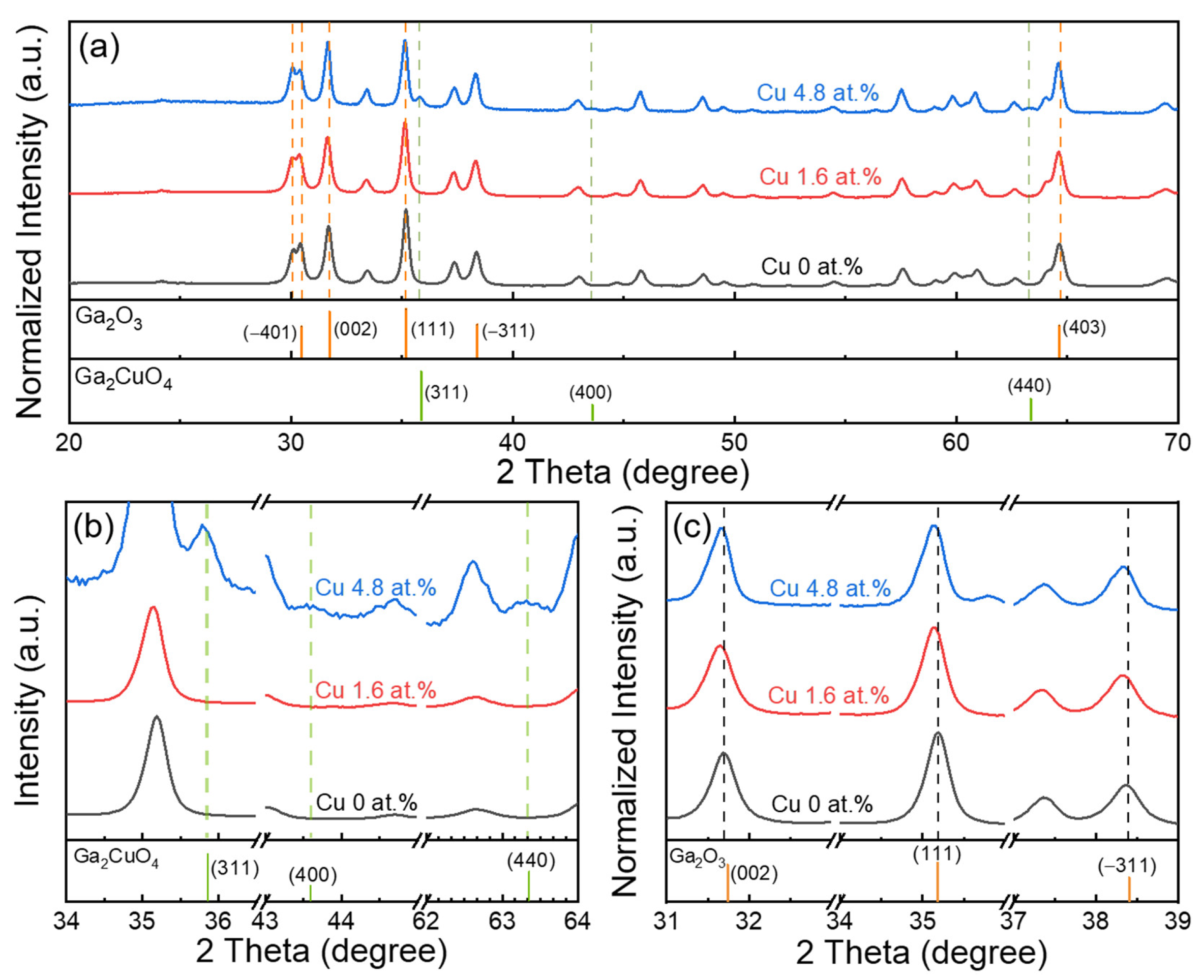
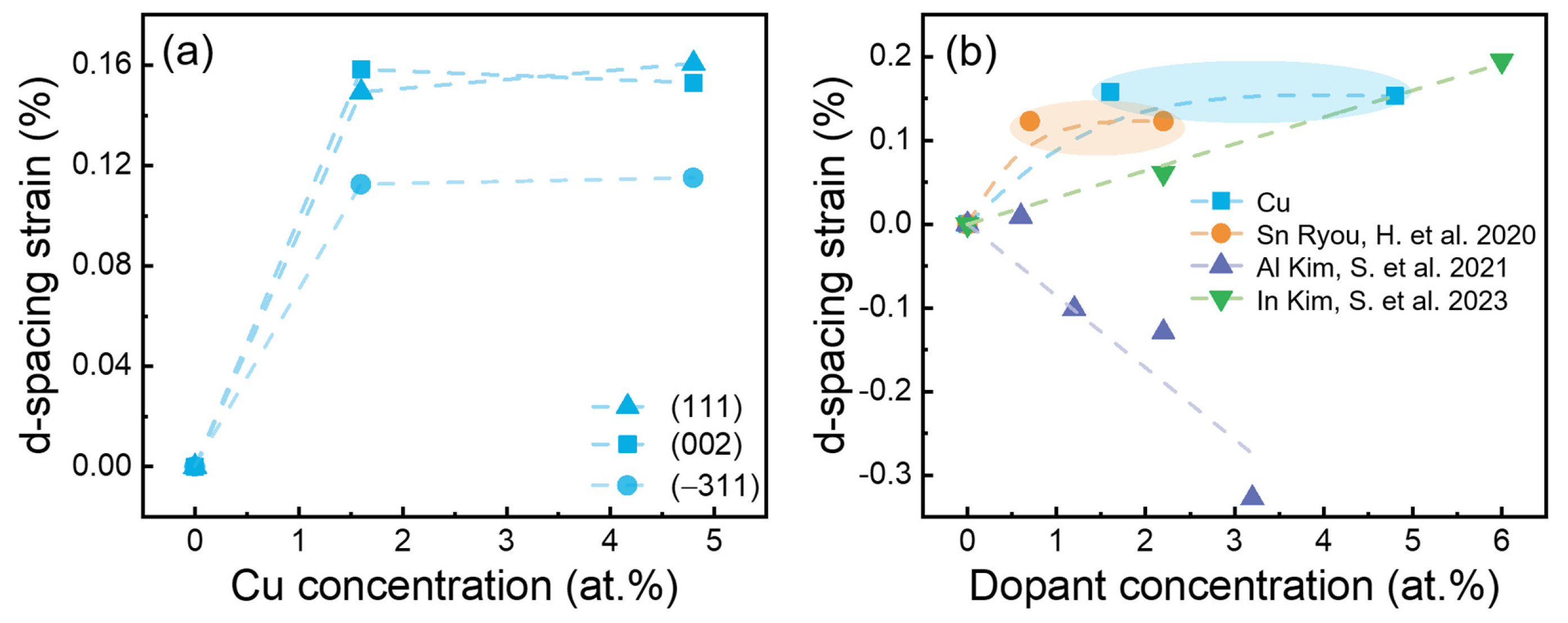
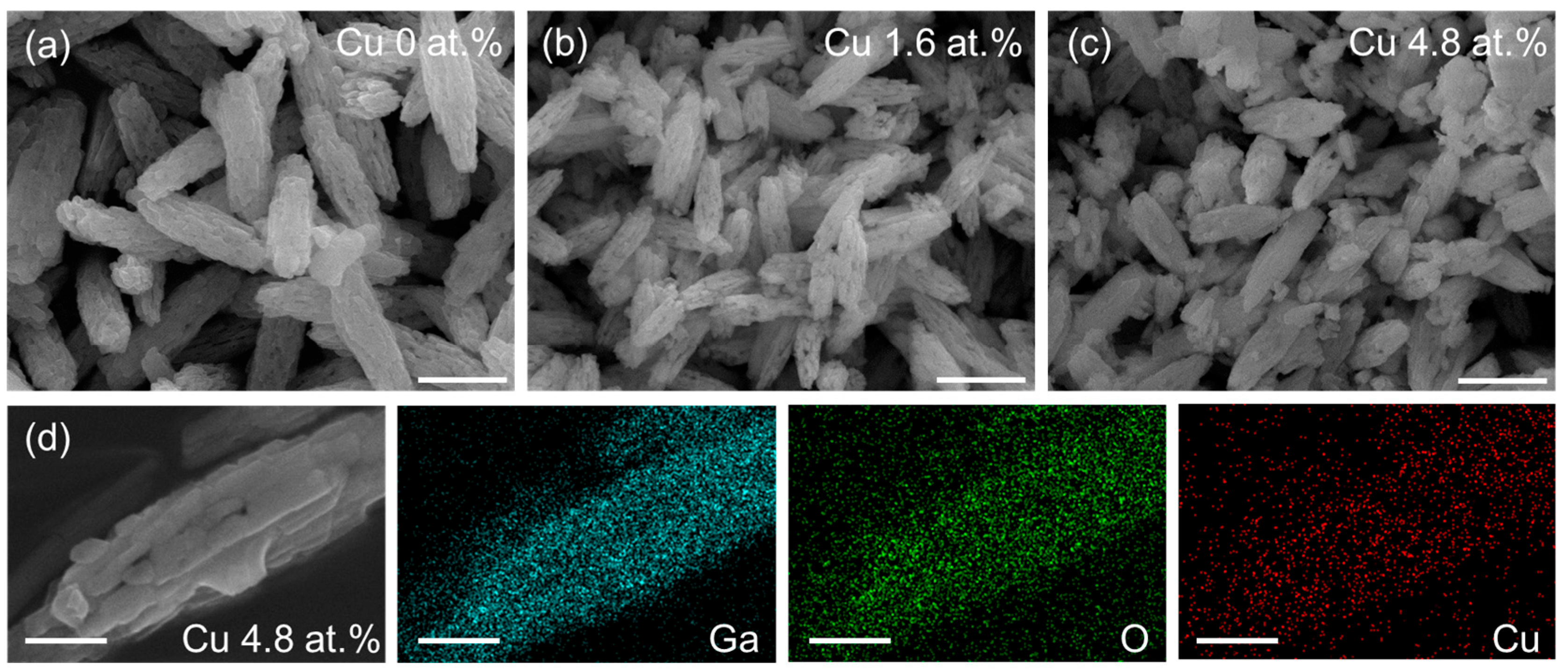
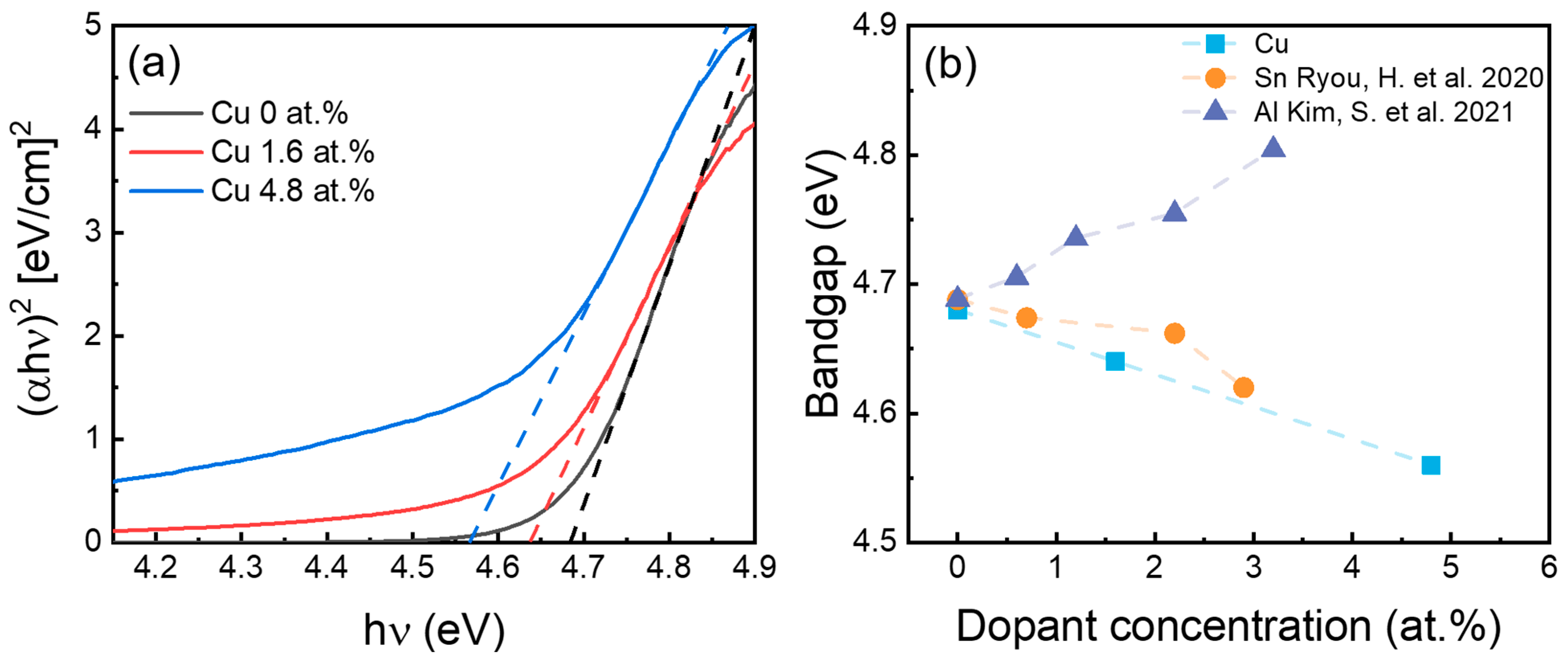
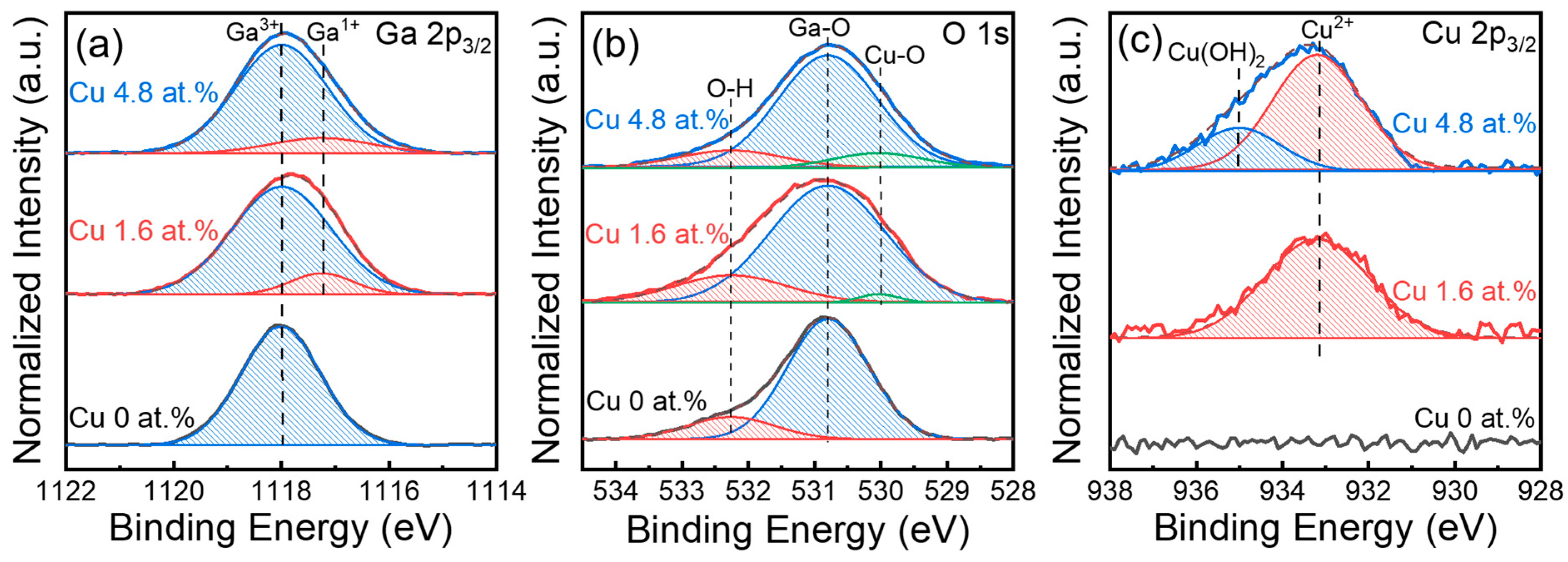
2. Results and Discussion

The crystallinity of Cu-doped β-Ga2O3 nanostructures with varying Cu concentrations was examined using XRD, as shown in Figure 1. Figure 1a displays the normalized XRD patterns of β-Ga2O3 samples with increasing Cu doping concentrations (0, 1.6, and 4.8 at.%). The dominant diffraction peaks corresponding to β-Ga2O3 were consistently observed across all samples, indicating that the host crystal structure was largely preserved despite increasing Cu content. However, at a doping level of 4.8 at.%, additional diffraction peaks appeared, which were indexed to Ga2CuO4. These secondary-phase peaks are further highlighted in Figure 1b. The results indicated that the solubility limit of Cu in β-Ga2O3 ranges from 1.6 to 4.8 at.%. A closer examination of the (002), (111), and (–311) planes of β-Ga2O3 in Figure 1c revealed a systematic shift toward lower 2θ values with increasing Cu concentration. At 1.6 at.% doping, the peak positions shifted to lower angles, and these shifts remained nearly unchanged at 4.8 at.% doping. This trend may be attributed to a possible increase in the lattice constant of β-Ga2O3 nanostructures resulting from the partial substitution of Ga3+ ions (ionic radius: 62 pm) with larger Cu2+ ions (ionic radius: 73 pm) [19,22]. However, alternative structural factors such as the formation of point defects, local lattice distortions, or stress relaxation effects may also contribute to the observed shift and cannot be excluded.
Figure 2a presents the d-spacing strain (%) of the (111), (002), and (–311) crystallographic planes in β-Ga2O3 nanostructures as a function of Cu concentration (at.%). The introduction of Cu atoms induced a positive d-spacing strain across all measured planes, indicating lattice expansion. This behavior was attributed to the substitutional incorporation of Cu atoms into Ga sites within the crystal lattice. Given that the ionic radii of Cu+ (0.77 Å) and Cu2+ (0.73 Å) are larger than that of Ga3+ (0.62 Å) [23], replacing Ga with Cu induces local lattice distortion. The resulting increase in interplanar spacing led to positive strain. Closer inspection of Figure 2a revealed that the d-spacing strain increased sharply with Cu concentration up to approximately 1.6 at.%, after which it began to saturate across all crystallographic planes. This saturation observed between 1.6 and 4.8 at.% indicated a limit to substitutional incorporation at higher doping levels, likely due to the formation of secondary phases arising from solubility limits that impede further lattice expansion. The corresponding peak positions are summarized in Table 1. At 4.8 at.% Cu, the emergence of minor peaks suggests the formation of a secondary phase, Ga2CuO4.
Figure 2b compares the d-spacing strain (%) induced by various dopants (Cu, Sn, Al, and In) as a function of dopant concentration (at.%). Cu, Sn, and In doping resulted in positive strain (lattice expansion), whereas Al doping led to negative strain (lattice contraction). These trends were primarily governed by the mismatch in ionic radii between the dopants and the host Ga3+ ion. Specifically, Cu+/Cu2+ and Sn4+ [11], which possess larger ionic radii than Ga3+, expand the lattice upon substitution. In contrast, Al3+ [12], having a smaller ionic radius, contracts the lattice. In3+ [14], with a slightly larger ionic radius than Ga3+, induces a gradual positive strain with increasing concentration.
The emergence of secondary-phase peaks corresponding to Ga2CuO4 in the XRD pattern at 4.8 at.% Cu doping indicates that the solubility limit of Cu in β-Ga2O3 has been exceeded. This interpretation is further supported by the (002) plane strain behavior shown in Figure 2a, where a saturation trend is observed beyond a certain Cu concentration. Such strain plateauing behavior is analogous to previous findings in Sn-doped β-Ga2O3 systems, where the precipitation of SnO2 beyond the solubility limit (approximately 1 at.%) was accompanied by a flattening of lattice strain and deterioration of photocatalytic performance [11]. In the present study, the morphological evolution (Figure 3) and the observed strain saturation collectively suggest that the formation of Ga2CuO4 is associated with structural distortion and possible degradation of material properties. Although localized techniques such as TEM or high-resolution XPS were not employed in this work, the XRD-based analysis provides strong evidence of bulk phase separation and strain relaxation. The secondary phase is expected to adversely affect the optical and electronic behavior of the nanostructures through interface scattering, localized defect states, or carrier trapping.
These findings underscored the critical role of dopant size in determining the direction and extent of lattice distortion in β-Ga2O3 nanostructures.
Interestingly, In and Al dopants induced continuous positive and negative strain trends, respectively, as the dopant concentration increased. In contrast, Cu and Sn doping exhibited a saturation behavior in strain. As shown for Cu in Figure 2a and previously reported for Sn-doped β-Ga2O3 [11], the strain initially increased with dopant concentration but eventually reached a plateau. This saturation behavior suggests that dopant atoms were substitutionally incorporated into the β-Ga2O3 lattice at lower concentrations. However, beyond a critical threshold—likely associated with the solubility limit or the onset of secondary phase formation—further incorporation became energetically unfavorable. Consequently, excess dopant atoms may segregate or form secondary phases, resulting in minimal additional lattice strain. This interpretation is supported by the experimental observation of secondary phases in the strain saturation region for both Cu and Sn doping in β-Ga2O3. SEM (JSM-7100F, JEOL, Tokyo, Japan) images of β-Ga2O3 nanostructures doped with different Cu concentrations are shown in Figure 3. The surface morphology remained relatively uniform across all doping levels, maintaining the characteristic rod-like features of hydrothermally synthesized β-Ga2O3. In the undoped sample (Figure 3a), the nanorods appeared uniform and isolated. Upon Cu doping at 1.6 at.% (Figure 3b), the rod-like morphology persisted, though a slight reduction in individual rod length and an increase in aggregation density were observed, implying partial suppression of anisotropic growth due to dopant incorporation. At 4.8 at.% Cu (Figure 3c), more pronounced morphological changes emerged, including the presence of small, dust-like particles surrounding the nanorods. This suggests that the Cu content at this concentration exceeded the solid solubility limit in β-Ga2O3, promoting the formation of secondary phases such as Ga2CuO4. These dust-like features, combined with structural broadening observed in XRD (Figure 1 and Figure 2), support the interpretation of strain saturation and lattice distortion at high doping levels.
To further verify the compositional uniformity, EDS elemental mapping was conducted for the 4.8 at.% Cu nanorod (Figure 3d). The Ga, O, and Cu elements are uniformly distributed, confirming successful Cu incorporation. While the SEM analysis was primarily qualitative, the observed trends in particle morphology, combined with structural and compositional evidence, strongly support the impact of Cu doping on crystal growth behavior.
The optical bandgap of Cu-doped β-Ga2O3 was estimated using Tauc plots in Figure 4a, which showed the relationship between the square of the absorption coefficient (αhν)2 and photon energy (hν).
It showed that as Cu concentration increased, the absorption edge shifted toward lower values, indicating a narrowing of the bandgap. Figure 4b summarizes the trends in optical bandgap values for three different dopants. The variation in the optical bandgap with different dopants could be understood by considering the intrinsic properties of the corresponding oxides—Al2O3, CuO (or Cu2O), and SnO2—as well as their effects on the crystal lattice and electronic structure of β-Ga2O3. Al doping led to an increase in the optical bandgap, which can be attributed to the large bandgap of Al2O3 (~6.9 eV) [24]. In contrast, Cu and Sn doping resulted in a reduction in the optical bandgap. This behavior can be explained by the relatively narrow bandgaps of CuO (~1.2–1.5 eV) [25] and SnO2 (~3.6 eV) [26] and the possible formation of defect states or secondary phases within the β-Ga2O3 matrix. In the case of Cu doping, the emergence of Ga2CuO4 secondary phases, as confirmed by XRD analysis, may contribute additional absorption pathways or introduce localized states within the bandgap. Recent studies have also shown that Cu doping in β-Ga2O3 can lead to a reduction in the optical bandgap, which has been attributed to the formation of impurity-induced energy levels. Zhang et al. [19] reported that post-annealed Cu-doped β-Ga2O3 films exhibited a significant narrowing of the bandgap, suggesting that Cu atoms were activated as acceptor-type impurities. These impurities introduce acceptor energy levels near the top of the valence band, thereby reducing the energy required for electronic transitions. This observation supports the hypothesis that Cu doping can effectively modify the electronic band structure by creating localized states, which contribute to bandgap narrowing. Similarly, Sn incorporation is known to form shallow donor states [27] or induce band tailing. These effects can lead to an apparent narrowing of the optical bandgap observed in the Tauc analysis. Therefore, the observed dopant-dependent bandgap modulation in β-Ga2O3 nanostructures is a combined result of lattice distortion, the ionic size and bandgap of the dopant oxide, and the formation of defect states or secondary phases.
The chemical states of Ga, O, and Cu in Cu-doped β-Ga2O3 nanostructures were analyzed using XPS, as shown in Figure 5. In the Ga 2p3/2 spectra in Figure 5a, the main peak centered at ~1118.2 eV corresponds to Ga3+ [28], characteristic of β-Ga2O3. A minor shoulder at a lower binding energy (~1117.2 eV) appears with increasing Cu concentration, which may be attributed to the formation of Ga1+ states [29], possibly induced by oxygen vacancies or Cu-related charge compensation effects. The O 1s spectra in Figure 5b were deconvoluted into three components: the dominant peak at ~530 eV associated with oxygen in CuO [30,31], a peak at ~530.8 eV corresponding to lattice O–Ga bonds [32], and a higher energy component (~532.3 eV) related to surface hydroxyl groups (O–H) [33]. The CuO-related peak becomes more prominent with Cu doping, indicating the increasing presence of Cu–O bonding environments within the nanostructure. The Cu 2p3/2 spectra in Figure 5c showed no detectable Cu signal in the undoped sample, as expected. In the Cu 1.6 at.% doped samples, broad peaks centered around 933.1 eV were observed, which is characteristic of Cu2+ ions [34]. This binding energy range is consistent with Cu–O bonds present in CuO or Cu2+ substituting Ga3+ sites within the Ga2O3 lattice. When Cu is incorporated into the Ga2O3 crystal structure, it likely replaces Ga3+ ions, leading to localized lattice distortions and the formation of Cu2+–O bonds. Additionally, the formation of Ga2CuO4, as confirmed by XRD analysis, contributes to this peak, as Cu2+ ions are a major constituent in this compound. In the 4.8 at.% doped samples, on top of the broad peaks centered around 933.1 eV, an additional peak around 935 eV was also observed, which is attributed to Cu(OH)2 or hydrated Cu species [35]. This observation implies that, at higher doping concentrations, Cu not only substitutes Ga in the β-Ga2O3 lattice as Cu2+ but may also contribute to the formation of secondary surface phases such as Ga2CuO4. Quantitative XPS analysis was performed, and the atomic ratios of Cu 2p, Ga 2p, and O 1s are shown in Table 2.
These results confirmed the incorporation of Cu into the β-Ga2O3 lattice and/or surface, along with the formation of Cu-based secondary phases, especially at higher doping concentrations. The presence of this peak suggested that, at higher Cu doping levels, some of the Cu atoms migrate to the surface or remain in an unincorporated state, reacting with adsorbed moisture or hydroxyl groups to form Cu(OH)2. This phenomenon could be observed when samples are exposed to ambient conditions or during the preparation process, where surface hydroxylation can occur. The formation of amorphous or poorly crystallized Cu(OH)2 would not produce detectable peaks in XRD, explaining why this component is only observed in the XPS spectra. This discrepancy can be explained by the surface-sensitive nature of XPS compared to the bulk-sensitive nature of XRD. XPS probes only the top few nanometers of the surface, where adsorbed or amorphous hydroxyl species may form due to exposure to ambient conditions or residual moisture during sample preparation. In contrast, XRD primarily detects long-range-ordered crystalline phases, and thus amorphous or low-concentration surface species like Cu(OH)2 may remain undetected.

3. Materials and Methods

3.1. Hydrothermal Synthesis of Cu-Doped β-Ga2O3 Nanostructures

To synthesize Cu-doped β-Ga2O3 nanostructures with varying doping concentrations, 0.1 M gallium (Ⅲ) nitrate hydrate (Ga(NO3)3·xH2O) was dissolved in 50 mL of deionized (DI) water using magnetic stirring at room temperature. CuCl2 was then added to obtain Cu/Ga atomic ratios of 0, 1.6, and 4.8 at.%. The initial pH of the solution was 2.14 and was adjusted to approximately 10 by adding ammonium hydroxide solution (NH4OH, 28 vol% in H2O). The solution was stirred at 300 RPM for 2 h at 60 °C and then transferred to a Teflon-lined stainless-steel autoclave, where it was heated in an electric oven at 140 °C for 10 h. After naturally cooling to room temperature, the resulting α-GaOOH nanostructures doped with various Cu concentrations were collected by centrifugation at 8000 RPM for 20 min. The collected precipitates were washed three times with DI water and subsequently dried in an oven at 70 °C for 6 h. Finally, the nanostructures were annealed in an O2 ambient at 1000 °C for 6 h to convert them to Cu-doped β-Ga2O3.

3.2. Characterization of Cu-Doped β-Ga2O3 Nanostructures

The crystal structure of Cu-doped β-Ga2O3 was characterized by XRD using Cu Kα radiation (λ = 1.5406 Å). XPS was employed to investigate the chemical bonding states of Cu within the nanostructures. The surface morphology and microstructural characteristics were examined using SEM, and the uniform distribution of dopants was further confirmed by energy-dispersive X-ray spectroscopy (EDS) analysis. The optical bandgap of the Cu-doped β-Ga2O3 nanostructures was estimated using the Tauc relation, as given in Equation (1) [36]:
( α h ν ) m = A ( h ν E g )
where α is the absorption coefficient [37], hν is the photon energy, A is a proportionality constant, Eg is the optical bandgap energy, and m is an index that depends on the nature of the electronic transition. For a direct allowed transition, m = ½ is used. To extract the bandgap, the linear portion of the (αhν)2 versus hν plot was fitted with a straight line of the form. The x-intercept of this line corresponds to the photon energy at which (αhν)2 = 0.

4. Conclusions

We synthesized Cu-doped β-Ga2O3 nanostructures using a hydrothermal method followed by annealing. XRD analysis confirmed that the β-Ga2O3 crystal structure was preserved at doping levels of 1.6 and 4.8 at.%. However, at 4.8 at.% doping, additional diffraction peaks appeared, which were identified as Ga2CuO4. At 1.6 at.% doping, the peak positions shifted to lower angles, and this shift remained nearly unchanged at 4.8 at.% doping. This observation suggests a possible increase in the lattice constant of β-Ga2O3 nanostructures due to the substitution of Ga3+ ions (ionic radius: 62 pm) with larger Cu2+ ions (ionic radius: 73 pm). The formation of secondary phases at higher doping levels further supports this conclusion. These results indicate that the solubility limit of Cu in β-Ga2O3 lies between 1.6 and 4.8 at.%. XPS analysis demonstrated that Cu was incorporated into the lattice as Cu2+, while surface-adsorbed Cu(OH)2 species were also detected at higher doping levels. Optical bandgap measurements revealed a reduction in the bandgap with increasing Cu concentration, likely due to defect state formation and contributions from secondary phases. This study provides valuable insights into the effects of Cu doping on β-Ga2O3, suggesting potential applications in tailoring optical properties for optoelectronic devices.

Author Contributions

Validation, S.K.; Formal analysis, J.L.; Investigation, J.K. and H.R.; Writing—review & editing, W.S.H. All authors have read and agreed to the published version of the manuscript.

Funding

This work was supported by the Korea Research Institute for Defense Technology Planning and Advancement (KRIT) grant funded by the Defense Acquisition Program Administration (DAPA) (Grant No. KRIT-CT-22−046) and also supported by the Korea Aerospace University grant funded by the Department of Materials Science and Engineering.

Institutional Review Board Statement

Not applicable.

Informed Consent Statement

Not applicable.

Data Availability Statement

The original contributions presented in the study are included in the article, further inquiries can be directed to the corresponding author.

Conflicts of Interest

The authors declare no conflicts of interest.

References

  1. Guo, D.; Guo, Q.; Chen, Z.; Wu, Z.; Li, P.; Tang, W. Review of Ga2O3-based optoelectronic devices. Mater. Today Phys. 2019, 11, 100157. [Google Scholar] [CrossRef]
  2. Zhang, J.; Shi, J.; Qi, D.C.; Chen, L.; Zhang, K.H. Recent progress on the electronic structure, defect, and doping properties of Ga2O3. APL Mater. 2020, 8, 020906. [Google Scholar] [CrossRef]
  3. Tsao, J.Y.; Chowdhury, S.; Hollis, M.A.; Jena, D.; Johnson, N.M.; Jones, K.A.; Kaplar, R.J.; Rajan, S.; Van de Walle, C.G.; Bellotti, E.; et al. Ultrawide-bandgap semiconductors: Research opportunities and challenges. Adv. Electron. Mater. 2018, 4, 1600501. [Google Scholar] [CrossRef]
  4. Yoshioka, S.; Hayashi, H.; Kuwabara, A.; Oba, F.; Matsunaga, K.; Tanaka, I. Structures and energetics of Ga2O3 polymorphs. J. Phys. Condens. Matter 2007, 19, 346211. [Google Scholar] [CrossRef]
  5. Pearton, S.J.; Yang, J.; Cary, P.H.; Ren, F.; Kim, J.; Tadjer, M.J.; Mastro, M.A. A review of Ga2O3 materials, processing, and devices. Appl. Phys. Rev. 2018, 5, 011301. [Google Scholar] [CrossRef]
  6. Biswas, M.; Nishinaka, H. Thermodynamically metastable α-, ε- (or κ-), and γ-Ga2O3: From material growth to device applications. APL Mater. 2022, 10, 060701. [Google Scholar] [CrossRef]
  7. Gao, S.; Li, W.; Dai, J.; Wang, Q.; Suo, Z. Effect of transition metals doping on electronic structure and optical properties of β-Ga2O3. Mater. Res. Express 2021, 8, 025904. [Google Scholar] [CrossRef]
  8. Kyrtsos, A.; Matsubara, M.; Bellotti, E. On the feasibility of p-type Ga2O3. Appl. Phys. Lett. 2018, 112, 032108. [Google Scholar] [CrossRef]
  9. Lyons, J.L. A survey of acceptor dopants for β-Ga2O3. Semicond. Sci. Technol. 2018, 33, 05LT02. [Google Scholar] [CrossRef]
  10. Suzuki, N.; Ohira, S.; Tanaka, M.; Sugawara, T.; Nakajima, K.; Shishido, T. Fabrication and characterization of transparent conductive Sn-doped β-Ga2O3 single crystal. Phys. Status Solidi C 2007, 4, 2310–2313. [Google Scholar] [CrossRef]
  11. Ryou, H.; Yoo, T.H.; Yoon, Y.; Lee, I.G.; Shin, M.; Cho, J.; Cho, B.J.; Hwang, W.S. Hydrothermal synthesis and photocatalytic property of Sn-doped β-Ga2O3 nanostructure. ECS J. Solid State Sci. Technol. 2020, 9, 045009. [Google Scholar] [CrossRef]
  12. Kim, S.; Ryou, H.; Lee, I.G.; Shin, M.; Cho, B.J.; Hwang, W.S. Impact of Al doping on a hydrothermally synthesized β-Ga2O3 nanostructure for photocatalysis applications. RSC Adv. 2021, 11, 7338–7346. [Google Scholar] [CrossRef]
  13. Ma, X.; Zhang, Y.; Dong, L.; Jia, R. First-principles calculations of electronic and optical properties of aluminum-doped β-Ga2O3 with intrinsic defects. Results Phys. 2017, 7, 1582–1589. [Google Scholar] [CrossRef]
  14. Kim, S.; Ryou, H.; Moon, J.; Lee, I.G.; Hwang, W.S. Codoping of Al and In atoms in β-Ga2O3 semiconductors. J. Alloys Compd. 2023, 931, 167502. [Google Scholar] [CrossRef]
  15. Kim, S.; Ryou, H.; Kim, H.W.; Hwang, W.S. Enhanced photocatalytic properties of Ge-doped Ga2O3 nanostructures synthesized via hydrothermal method. Semicond. Sci. Technol. 2025, 40, 035003. [Google Scholar] [CrossRef]
  16. Saleh, M.; Bhattacharyya, A.; Varley, J.B.; Swain, S.; Jesenovec, J.; Krishnamoorthy, S.; Lynn, K. Electrical and optical properties of Zr doped β-Ga2O3 single crystals. Appl. Phys. Express 2019, 12, 085502. [Google Scholar] [CrossRef]
  17. Yoo, T.H.; Ryou, H.; Lee, I.G.; Cho, B.J.; Hwang, W.S. Enhanced photocatalytic activity of electrospun β-Ga2O3 nanofibers via in-situ Si doping using tetraethyl orthosilicate. Catalysts 2019, 9, 1005. [Google Scholar] [CrossRef]
  18. Zheng, T.; Wang, Q.; Dang, J.; He, W.; Wang, L.; Zheng, S. Effects of Si concentration on electronic structure and optical gap of Si-doped β-Ga2O3. Comput. Mater. Sci. 2020, 174, 109505. [Google Scholar] [CrossRef]
  19. Zhang, Y.; Yan, J.; Li, Q.; Qu, C.; Zhang, L.; Xie, W. Optical and structural properties of Cu-doped β-Ga2O3 films. Mater. Sci. Eng. B 2011, 176, 846–849. [Google Scholar] [CrossRef]
  20. Yan, H.; Guo, Y.; Song, Q.; Chen, Y. First-Principles Study on Electronic Structure and Optical Properties of Cu-Doped β-Ga2O3. Phys. B Condens. Matter 2014, 434, 181–184. [Google Scholar] [CrossRef]
  21. Gong, G.; Gou, L. Microstructure and Properties of Cu-Doped β-Ga2O3 Rod Prepared with Liquid Metallic Gallium. J. Eur. Ceram. Soc. 2025, 45, 116916. [Google Scholar] [CrossRef]
  22. Chen, Y.; Yang, F.; Duan, J.; Meng, H.; Zhang, W.; Luo, W.; Wu, Y.; Wang, Y.; Zhang, Y. Band engineering of ReS2/V-In2S3 S-scheme heterojunction for high-efficiency visible-light-driven hydrogen evolution. Chem. Eng. J. 2025, 514, 163380. [Google Scholar] [CrossRef]
  23. Babu, A.; Rao, N.M. Effect of Copper Substitution on the Structural, Optical, and Magnetic Properties of β-Ga2O3 Powders. Appl. Phys. A 2025, 131, 172. [Google Scholar] [CrossRef]
  24. Kamimura, T.; Sasaki, K.; Wong, M.H.; Krishnamurthy, D.; Kuramata, A.; Masui, T.; Yamakoshi, S.; Higashiwaki, M. Band Alignment and Electrical Properties of Al2O3/β-Ga2O3 Heterojunctions. Appl. Phys. Lett. 2014, 104, 192104. [Google Scholar] [CrossRef]
  25. Oruç, Ç.; Altındal, A. Structural and Dielectric Properties of CuO Nanoparticles. Ceram. Int. 2017, 43, 10708–10714. [Google Scholar] [CrossRef]
  26. Akgul, F.A.; Gumus, C.; Ali, O.E.; Farha, A.H.; Akgul, G.; Ufuktepe, Y.; Liu, Z. Structural and Electronic Properties of SnO2. J. Alloys Compd. 2013, 579, 50–56. [Google Scholar] [CrossRef]
  27. Chikoidze, E.; von Bardeleben, H.J.; Akaiwa, K.; Shigematsu, E.; Kaneko, K.; Fujita, S.; Dumont, Y. Electrical, Optical, and Magnetic Properties of Sn Doped α-Ga2O3 Thin Films. J. Appl. Phys. 2016, 120, 025109. [Google Scholar] [CrossRef]
  28. Suri, R.; Lichtenwalner, D.J.; Misra, V. Interfacial Self Cleaning during Atomic Layer Deposition and Annealing of HfO2 Films on Native (100)-GaAs Substrates. Appl. Phys. Lett. 2010, 96, 112905. [Google Scholar] [CrossRef]
  29. Yang, L.X.; Zhao, X.; Xu, S.; Lu, Y.Y.; Chang, H.; Liu, J. Oxide Transformation and Break-Up of Liquid Metal in Boiling Solutions. Sci. China Technol. Sci. 2020, 63, 289–296. [Google Scholar] [CrossRef]
  30. Chen, R.X.; Zhu, S.L.; Mao, J.; Cui, Z.D.; Yang, X.J.; Liang, Y.Q.; Li, Z.Y. Synthesis of CuO/Co3O4 Coaxial Heterostructures for Efficient and Recycling Photodegradation. Int. J. Photoenergy 2015, 1, 183468. [Google Scholar]
  31. Shao, P.R.; Deng, S.Z.; Chen, J.; Chen, J.; Xu, N.S. Study of Field Emission, Electrical Transport, and Their Correlation of Individual Single CuO Nanowires. J. Appl. Phys. 2011, 109, 023710. [Google Scholar] [CrossRef]
  32. Makeswaran, N.; Battu, A.K.; Swadipta, R.; Manciu, F.S.; Ramana, C.V. Spectroscopic Characterization of the Electronic Structure, Chemical Bonding, and Band Gap in Thermally Annealed Polycrystalline Ga2O3 Thin Films. ECS J. Solid State Sci. Technol. 2019, 8, Q3249. [Google Scholar] [CrossRef]
  33. Dhaka, R.; Yadav, A.; Pal, P.; Prakash, C.; Gupta, G.; Dixit, A.; Dutta, S.; Shukla, A.K. Growth of β-Ga2O3-ZnO Nanowires Heterostructure on Si Substrate for UV-Visible Multi-Band Photodetector Applications. 2024. Available online: https://ssrn.com/abstract=4988085 (accessed on 4 April 2025).
  34. Tang, C.; Dong, H. The Effects of Cu2+ Adsorption on Surface Dissolution of Albite. Colloids Surf. A Physicochem. Eng. Asp. 2022, 644, 128832. [Google Scholar] [CrossRef]
  35. Wang, X.; Zhang, B.; Zhang, W.; Yu, M.; Cui, L.; Cao, X.; Liu, J. Super-light Cu@Ni nanowires/graphene oxide composites for significantly enhanced microwave absorption performance. Sci. Rep. 2017, 7, 1584. [Google Scholar] [CrossRef] [PubMed]
  36. Tumuluri, A.; Naidu, K.L.; Raju, K.J. Band gap determination using Tauc’s plot for LiNbO3 thin films. Int. J. ChemTech Res. 2014, 6, 3353–3356. [Google Scholar]
  37. George, P.; Chowdhury, P. Complex Dielectric Transformation of UV-Vis Diffuse Reflectance Spectra for Estimating Optical Band-Gap Energies and Materials Classification. Analyst 2019, 144, 3005–3012. [Google Scholar] [CrossRef]
Figure 1. X-ray diffraction (XRD) patterns of Cu-doped β-Ga2O3 nanostructures with different Cu concentrations (0, 1.6, and 4.8 at.%). (a) Full-range XRD patterns compared with reference peaks for β-Ga2O3 (PDF Card No. 00-043-1012) and Ga2CuO4 (PDF Card No. 01-078-0172). (b) Magnified view of selected diffraction regions highlighting the (311), (400), and (440) planes of Ga2CuO4. (c) Enlarged view of the (002), (111), and (–311) planes of β-Ga2O3, showing a progressive shift in the main peaks toward lower 2θ values with increasing Cu content.
Inorganics 13 00231 g001
Figure 2. (a) d-spacing strain (%) of the (111), (002), and (–311) crystallographic planes in β-Ga2O3 nanostructures as a function of Cu concentration (at.%). (b) Comparison of d-spacing strain (%) induced by various dopants (Cu, Sn, Al, and In) as a function of dopant concentration (at.%). For Cu, Sn [11], and Al [12], the strain values are derived from the (002) plane, whereas the values for In [14] represent the average strain across multiple crystallographic planes. The shaded regions indicate dopant concentration ranges where secondary phase formation is observed.
Inorganics 13 00231 g002
Figure 3. SEM images (Scale bar: 1 µm) of β-Ga2O3 nanostructures doped with varying Cu concentrations: (a) 0 at.%, (b) 1.6 at.%, and (c) 4.8 at.%. (d) SEM image (scale bars: 250 nm) of a single nanostructure from the Cu 4.8 at.% sample and corresponding EDS elemental map (scale bars: 250 nm) ping showing the spatial distributions of Ga (cyan), O (green), and Cu (red). The uniform presence of Cu confirms its successful incorporation.
Inorganics 13 00231 g003
Figure 4. (a) Tauc plots of (αhν)2 versus photon energy (hν) for β-Ga2O3 nanostructures doped with different Cu concentrations (0, 1.6, and 4.8 at.%). The optical bandgap is determined by the linear extrapolation of the absorption edge to the X-axis (photon energy axis) in the Tauc plot. (b) Comparison of the extracted optical bandgap values as a function of dopant concentration for Cu-, Sn- [11], and Al-doped β-Ga2O3 [12]. Cu and Sn doping result in a decrease in bandgap, whereas Al doping leads to bandgap widening.
Inorganics 13 00231 g004
Figure 5. XPS spectra of β-Ga2O3 nanostructures with different Cu doping concentrations (0, 1.6, and 4.8 at.%): (a) Ga 2p3/2 core level showing the relative contributions of Ga3+ and Ga1+ oxidation states, (b) O 1s core level deconvoluted into O-Ga-, O-H-, and O-Cu-related components, and (c) Cu 2p3/2 core level, indicating the presence of Cu(OH)2 and CuO (or Ga2CuO4-like bonding) species at higher doping concentrations.
Inorganics 13 00231 g005
Table 1. Diffraction peak positions of the main β-Ga2O3 planes (002), (111), and (–311) as a function of Cu doping concentration.
Cu DopingPlane
(002)(111)(–311)
0 at.%31.68731.64831.648
1.6 at.%35.19335.15435.114
4.8 at.%38.34438.30538.344
Table 2. Atomic ratios of Cu 2p, Ga 2p, and O 1s obtained from XPS quantification as a function of Cu doping concentration. The measured Cu content matches well with the nominal doping levels, supporting the effective incorporation of Cu into the β-Ga2O3 nanostructures.
Cu DopingAtomic Ratio from XPS Quantification
Cu 2pGa 2pO 1s
0 at.%0%29.7%70.3%
1.6 at.%1.6%26.3%72.1%
4.8 at.%4.8%50%45.2%
Disclaimer/Publisher’s Note: The statements, opinions and data contained in all publications are solely those of the individual author(s) and contributor(s) and not of MDPI and/or the editor(s). MDPI and/or the editor(s) disclaim responsibility for any injury to people or property resulting from any ideas, methods, instructions or products referred to in the content.

