

Enhancing Optoelectronic Properties of Multicrystalline Silicon Using Dual Treatments for Solar Cell Applications


Abstract
1. Introduction
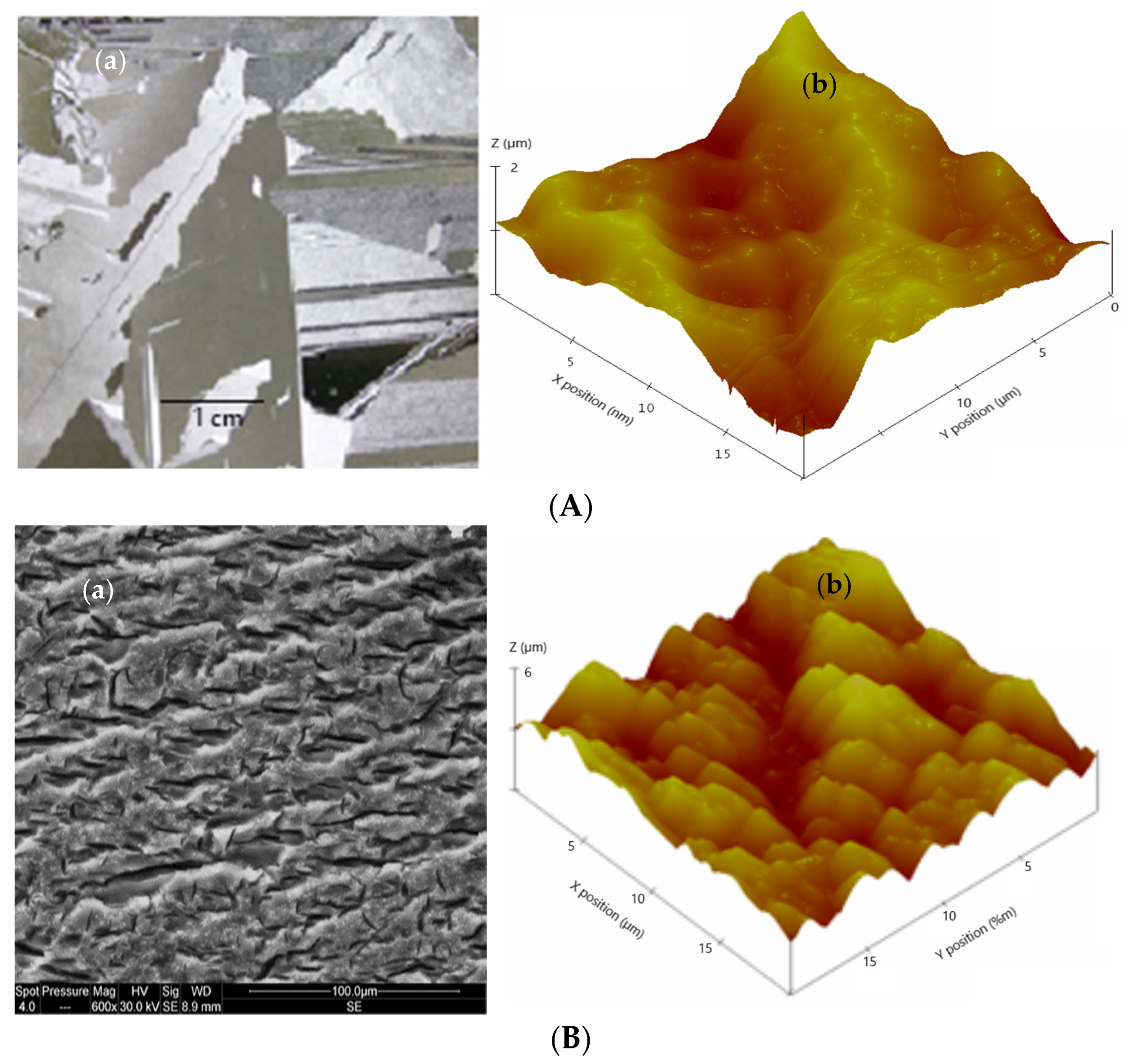
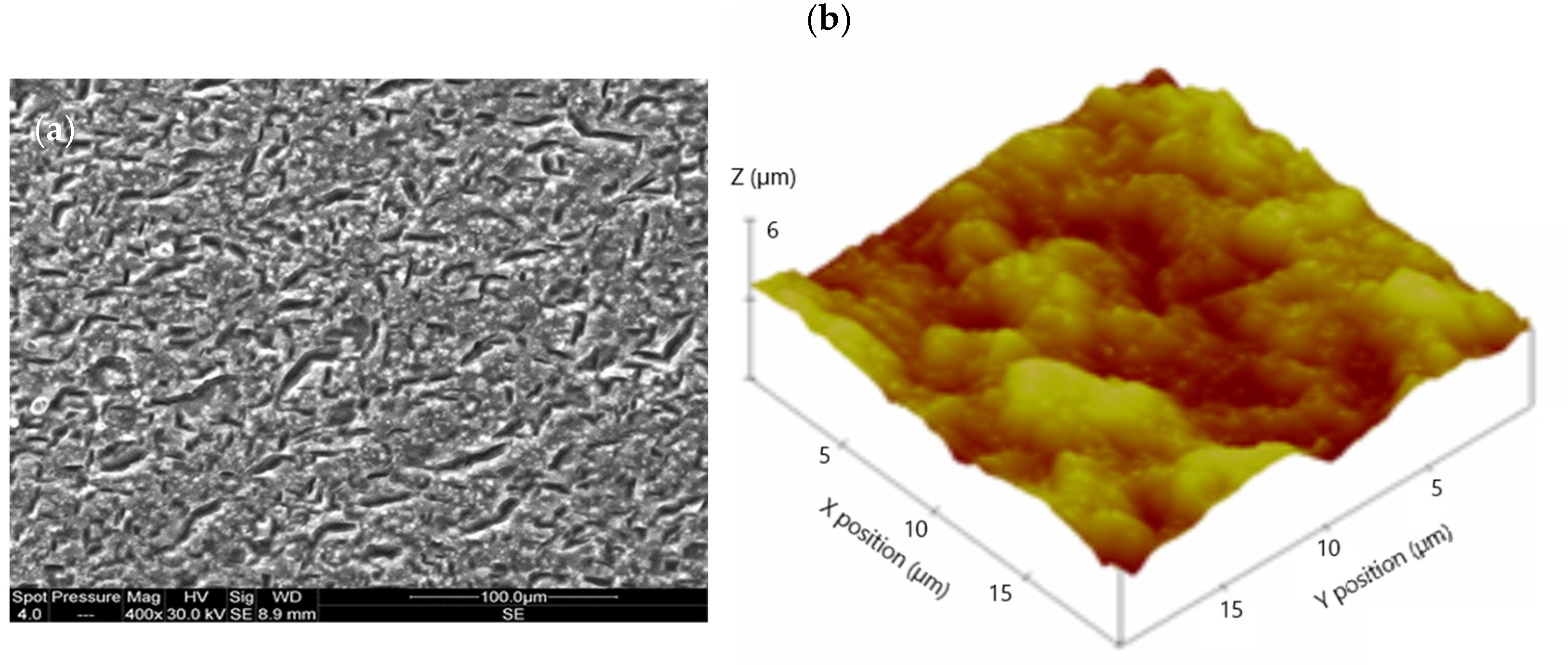
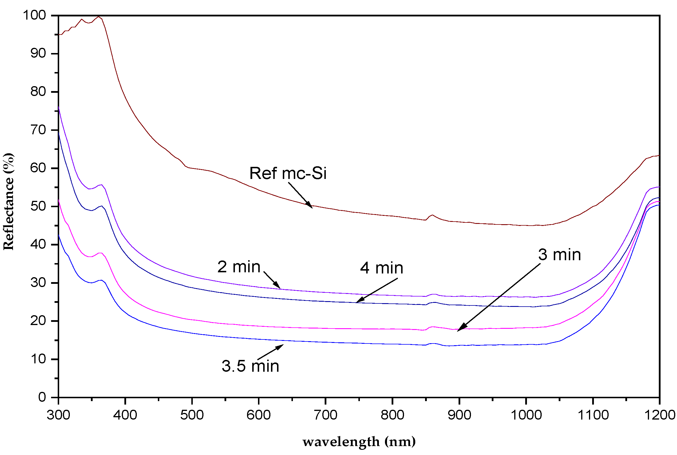
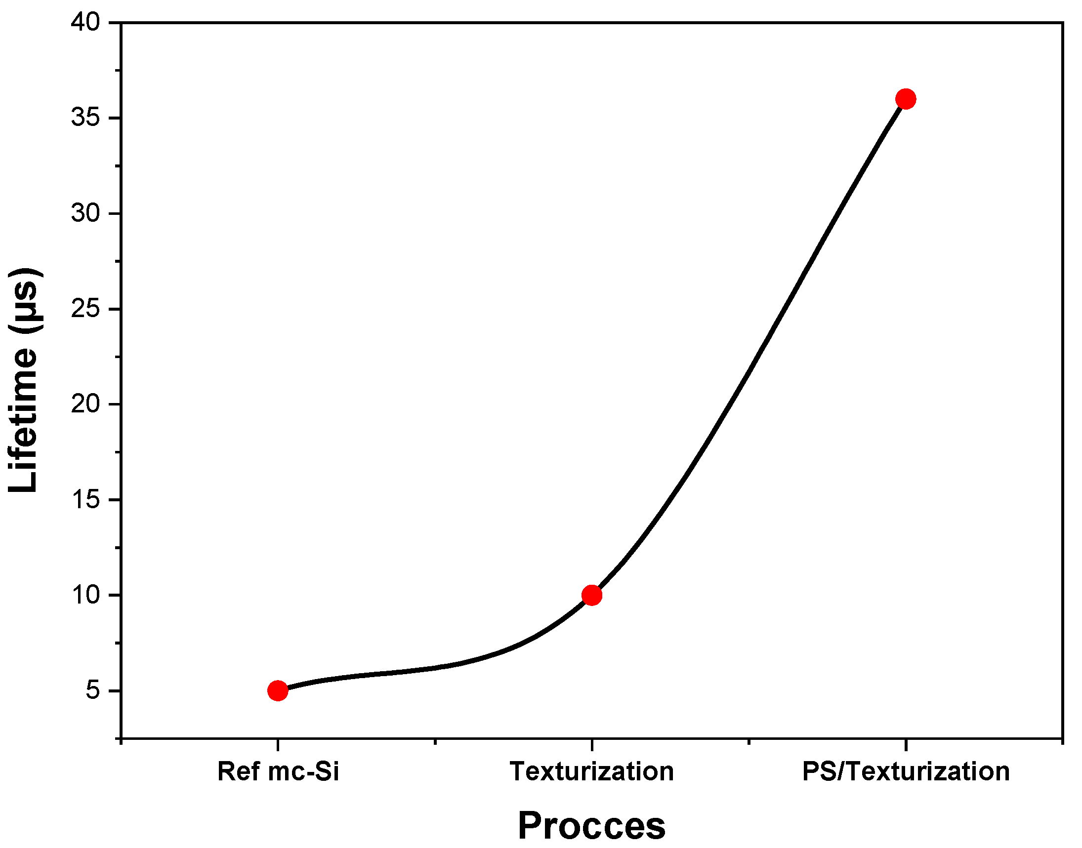
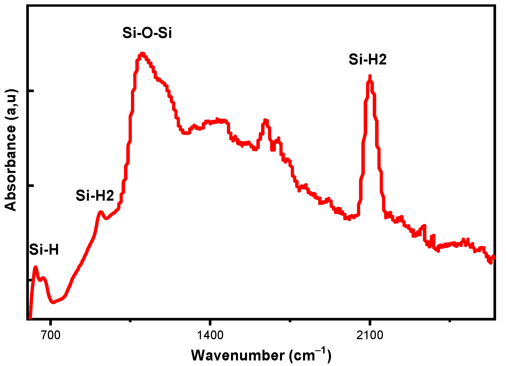
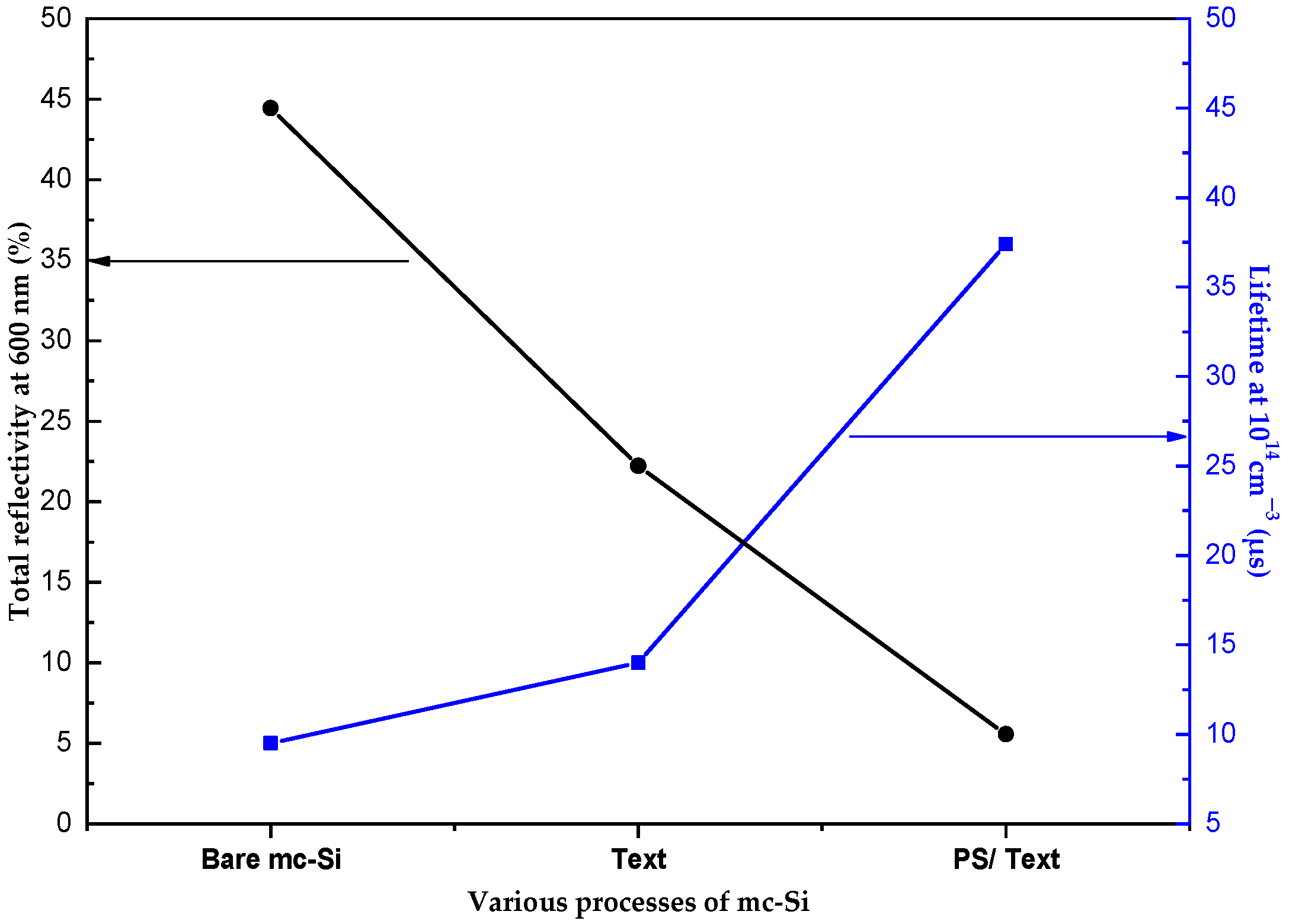
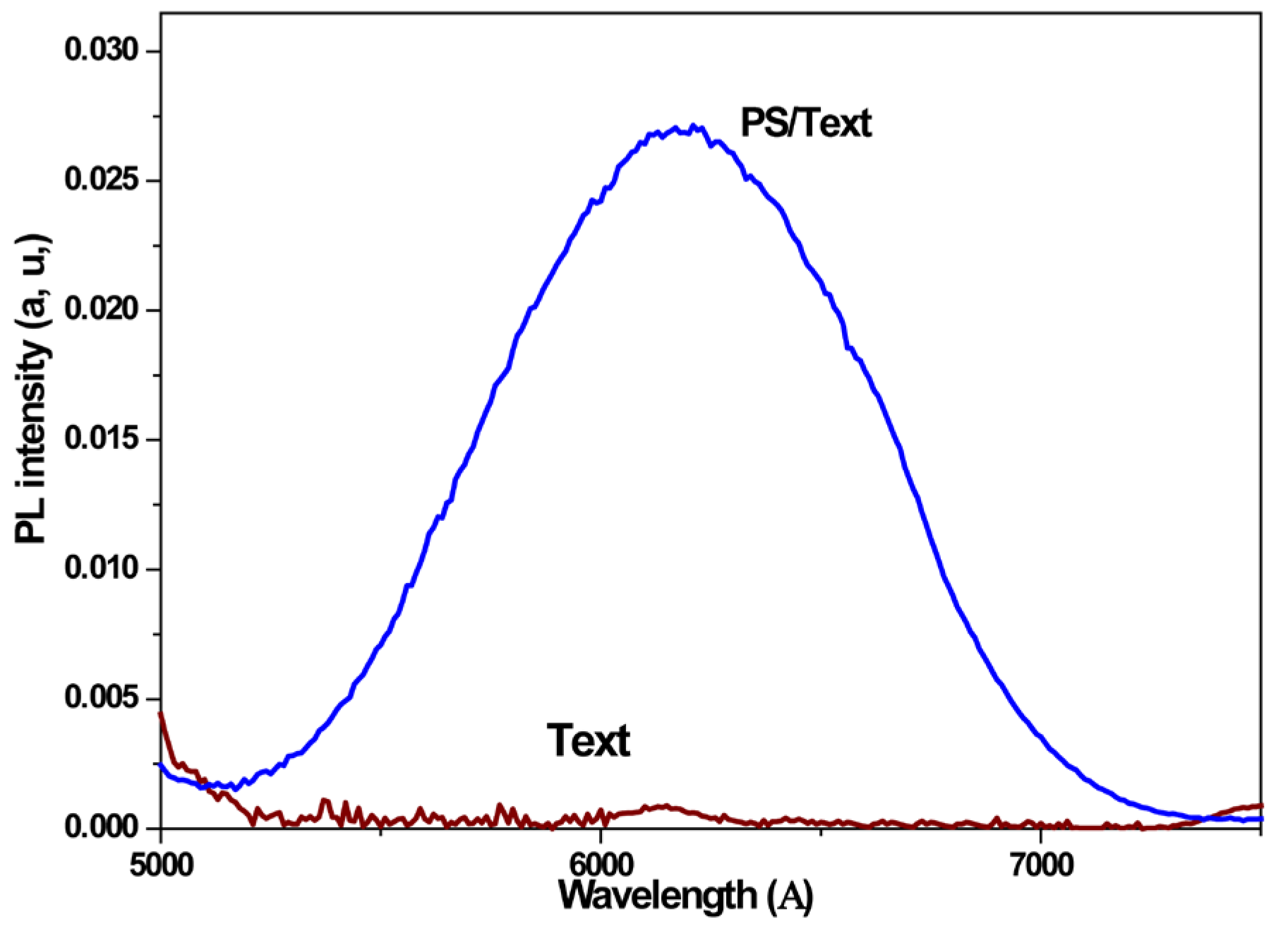
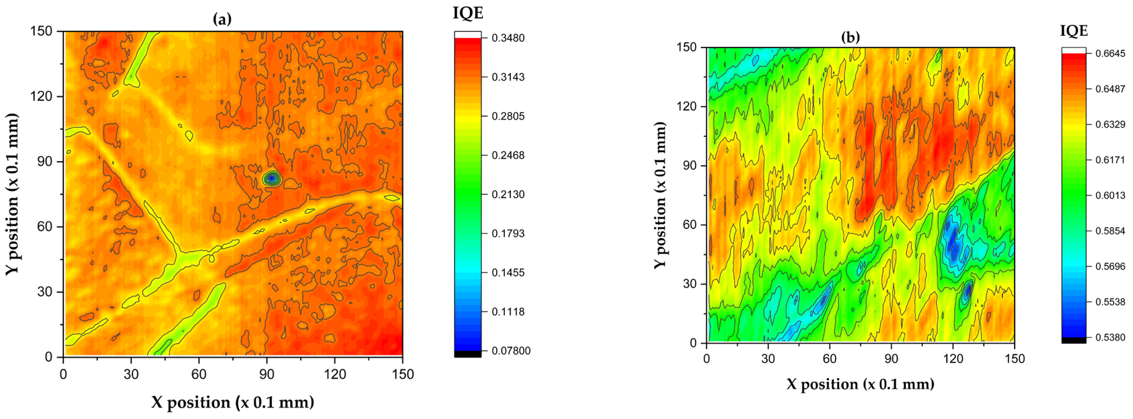
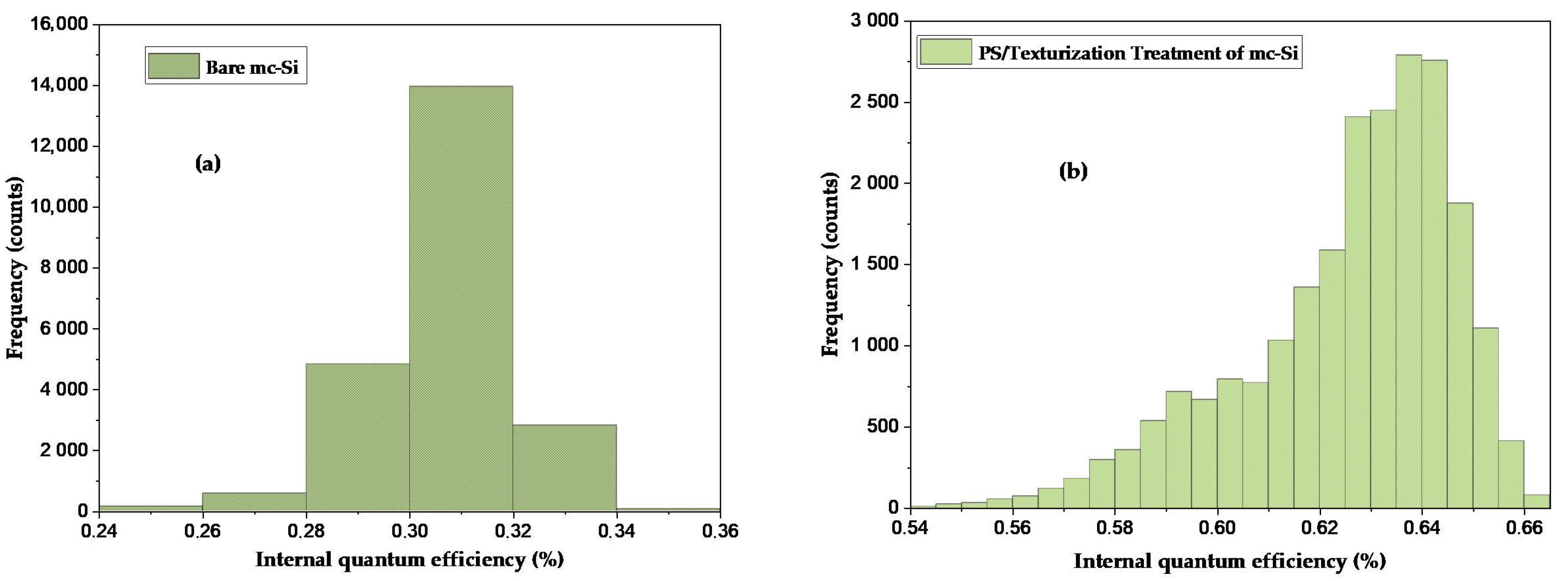
2. Results
3. Materials and Methods
4. Conclusions
Author Contributions
Funding
Institutional Review Board Statement
Informed Consent Statement
Data Availability Statement
Conflicts of Interest
References
- Schindler, F.; Michl, B.; Krenckel, P.; Riepe, S.; Benick, J.; Müller, R.; Schubert, M.C. Optimized multicrystalline silicon for solar cells enabling conversion efficiencies of 22%. Sol. Energy Mater. Sol. Cells 2017, 171, 180–186. [Google Scholar] [CrossRef]
- Schindler, F.; Fell, A.; Müller, R.; Benick, J.; Richter, A.; Feldmann, F.; Glunz, S.W. Towards the efficiency limits of multicrystalline silicon solar cells. Sol. Energy Mater. Sol. Cells 2018, 185, 198–204. [Google Scholar] [CrossRef]
- Möller, H.J.; Funke, C.; Rinio, M.; Scholz, S. Multicrystalline silicon for solar cells. Thin Solid Film. 2005, 487, 179–187. [Google Scholar] [CrossRef]
- Gurusamy, A.; Manickam, S.; Perumalsamy, R. Quality improvement of multi-crystalline silicon ingot by the Hot-Zone modification. J. Cryst. Growth 2022, 592, 126720. [Google Scholar] [CrossRef]
- Koynov, S.; Brandt, M.S.; Stutzmann, M. Black multi-crystalline silicon solar cells. Phys. Status Solidi (RRL)–Rapid Res. Lett. 2007, 1, R53–R55. [Google Scholar] [CrossRef]
- Alrasheedi, N.H. The effects of porous silicon and silicon nitride treatments on the electronic qualities of multicrystalline silicon for solar cell applications. Silicon 2024, 16, 1765–1773. [Google Scholar] [CrossRef]
- Rabha, M.B.; El Haj, A.; Mannai, A.; Choubani, K.; Almeshaal, M.A.; Dimassi, W. Optoelectronic proprieties improvement of multicrystalline silicon by Alumina Nanoparticles and silicon nitride. Preprints 2025, in press. [Google Scholar] [CrossRef]
- Park, K.M.; Jung, J.H.; Hong, J.E.; Choi, S.Y.; Lee, M.B. RIE Texturing Optimization for Multicrystalline Silicon Solar Cell. In ECS Meeting Abstracts; IOP Publishing: Bristol, UK, 2010; Volume 1, p. 62. [Google Scholar]
- Valiei, M.; Shaibani, P.M.; Abdizadeh, H.; Kolahdouz, M.; Soleimani, E.A.; Poursafar, J. Design and optimization of single, double and multilayer anti-reflection coatings on planar and textured surface of silicon solar cells. Mater. Today Commun. 2022, 32, 104144. [Google Scholar] [CrossRef]
- Solanki, C.S.; Singh, H.K.; Solanki, C.S.; Singh, H.K. Anti-reflection Coatings with Textured Surface for c-Si Solar Cells. In Anti-Reflection and Light Trapping in c-Si Solar Cells; Springer: Berlin/Heidelberg, Germany, 2017; pp. 99–114. [Google Scholar]
- Almeshaal, M.A.; Abdouli, B.; Choubani, K.; Khezami, L.; Rabha, M.B. Study of porous silicon layer effect in optoelectronics properties of multi-crystalline silicon for photovoltaic applications. Silicon 2023, 15, 6025–6032. [Google Scholar] [CrossRef]
- Yoo, J.; Cho, J.; Han, K.; Yi, J. RIE surface texturing for optimum light trapping in multicrystalline silicon solar cells. J. Korean Phys. Soc. 2012, 60, 2071–2074. [Google Scholar] [CrossRef]
- Yousuf, H.; Rahman, R.U.; Jang, S.; Rehan, S.; Khokhar, M.Q.; Park, S.; Yi, J. Enhanced hydrogenated silicon nitride (SiNx: H) thin film as single layer anti-reflection (SLAR) coating in tunnel oxide passivated contact solar cells. Mater. Sci. Semicond. Process. 2025, 192, 109483. [Google Scholar]
- Rathinavelu, V.; Upadhyay, V.V.; Prabagaran, S.; Govindarajan, S.; Verma, A.; Soudagar, M.E.M.; Seikh, A.H. Texturing of silicon nitride passivation layers on functional behaviour study of polycrystalline silicon (p-Si) made with plasma enhanced chemical vapour deposition. J. Mater. Sci. Mater. Electron. 2025, 36, 73. [Google Scholar] [CrossRef]
- Çiftci, B.G.; Güldür, Ç.; Güneş, S. Inverted Pyramid Texturization of Monocrystalline Silicon Surface by Cu-Assisted Chemical Etching at Different Conditions. Silicon 2025. [Google Scholar] [CrossRef]
- Stapf, A.; Gondek, C.; Kroke, E.; Roewer, G. Wafer cleaning, etching, and texturization. In Handbook of Photovoltaic Silicon; Springer: Berlin/Heidelberg, Germany, 2019; pp. 311–358. [Google Scholar]
- Raji, M.; Gurusamy, A.; Manikkam, S.; Perumalsamy, R. Monocrystalline Silicon Wafer Recovery Via Chemical Etching from End-of-Life Silicon Solar Panels for Solar Cell Application. Silicon 2024, 16, 3669–3688. [Google Scholar] [CrossRef]
- Marrero, N.; Guerrero-Lemus, R.; Gonzalez-Diaz, B.; Borchert, D. Effect of porous silicon stain etched on large area alkaline textured crystalline silicon solar cells. Thin Solid Film. 2009, 517, 2648–2650. [Google Scholar] [CrossRef]
- Bilyalov, R.R.; Lüdemann, R.; Wettling, W.; Stalmans, L.; Poortmans, J.; Nijs, J.; Lévy-Clément, C. Multicrystalline silicon solar cells with porous silicon emitter. Sol. Energy Mater. Sol. Cells 2000, 60, 391–420. [Google Scholar] [CrossRef]
- Montesdeoca-Santana, A.; Gonzalez-Diaz, B.; Jiménez-Rodríguez, E.; Ziegler, J.; Velázquez, J.J.; Hohage, S.; Guerrero-Lemus, R. Influence of stain etching on low minority carrier lifetime areas of multicrystalline silicon for solar cells. Mater. Sci. Eng. B 2011, 176, 1541–1545. [Google Scholar] [CrossRef]
- Gupta, I.; Colvin, V.L.; George, S.M. Hydrogen desorption kinetics from monohydride and dihydride species on silicon surfaces. Phys. Rev. B 1988, 37, 8234. [Google Scholar] [CrossRef]
- Montero, I.; Galan, L.; Najmi, O.; Albella, J.M. Disorder-induced vibration-mode coupling in SiO2 films observed under normal-incidence infrared radiation. Phys. Rev. B 1994, 50, 4881. [Google Scholar] [CrossRef]
- Rabha, M.B.; Bessaïs, B. Enhancement of photovoltaic properties of multicrystalline silicon solar cells by combination of buried metallic contacts and thin porous silicon. Sol. Energy 2010, 84, 486–491. [Google Scholar] [CrossRef]
- Rabha, M.B.; Dimassi, W.; Bouaïcha, M.; Ezzaouia, H.; Bessais, B. Laser-beam-induced current mapping evaluation of porous silicon-based passivation in polycrystalline silicon solar cells. Sol. Energy 2009, 83, 721–725. [Google Scholar] [CrossRef]
- Dimassi, W.; Derbali, L.; Bouaıcha, M.; Bessaıs, B.; Ezzaouia, H. Two-dimensional LBIC and Internal-Quantum-Efficiency investigations of grooved grain boundaries in multicrystalline silicon solar cells. Sol. Energy 2011, 85, 350–355. [Google Scholar] [CrossRef]
- Abdouli, B.; Khezami, L.; Guesmi, A.; Assadi, A.A.; Rabha, M.B. Numerical and experimental study of the front surface recombination velocities and base widths effect in multi-crystalline silicon solar cell quantum efficiency. Crystals 2023, 13, 425. [Google Scholar] [CrossRef]
- Achref, M.; Khezami, L.; Mokraoui, S.; Rabha, M.B. Effective surface passivation on multi-crystalline silicon using aluminum/porous silicon nanostructures. Surf. Interfaces 2020, 18, 100391. [Google Scholar] [CrossRef]


| Process | Bare mc-Si | Texturized mc-Si | Texturized/PS |
|---|---|---|---|
| Lifetime (µs) | 2 | 10 | 36 |
Disclaimer/Publisher’s Note: The statements, opinions and data contained in all publications are solely those of the individual author(s) and contributor(s) and not of MDPI and/or the editor(s). MDPI and/or the editor(s) disclaim responsibility for any injury to people or property resulting from any ideas, methods, instructions or products referred to in the content. |
© 2025 by the authors. Licensee MDPI, Basel, Switzerland. This article is an open access article distributed under the terms and conditions of the Creative Commons Attribution (CC BY) license (https://creativecommons.org/licenses/by/4.0/).
Share and Cite
Choubani, K.; Zouari, Y.; El Haj, A.; Mannai, A.; Almeshaal, M.A.; Dimassi, W.; Ben Rabha, M. Enhancing Optoelectronic Properties of Multicrystalline Silicon Using Dual Treatments for Solar Cell Applications. Inorganics 2025, 13, 142. https://doi.org/10.3390/inorganics13050142
Choubani K, Zouari Y, El Haj A, Mannai A, Almeshaal MA, Dimassi W, Ben Rabha M. Enhancing Optoelectronic Properties of Multicrystalline Silicon Using Dual Treatments for Solar Cell Applications. Inorganics. 2025; 13(5):142. https://doi.org/10.3390/inorganics13050142
Chicago/Turabian StyleChoubani, Karim, Yasmin Zouari, Ameny El Haj, Achref Mannai, Mohammed A. Almeshaal, Wissem Dimassi, and Mohamed Ben Rabha. 2025. "Enhancing Optoelectronic Properties of Multicrystalline Silicon Using Dual Treatments for Solar Cell Applications" Inorganics 13, no. 5: 142. https://doi.org/10.3390/inorganics13050142
APA StyleChoubani, K., Zouari, Y., El Haj, A., Mannai, A., Almeshaal, M. A., Dimassi, W., & Ben Rabha, M. (2025). Enhancing Optoelectronic Properties of Multicrystalline Silicon Using Dual Treatments for Solar Cell Applications. Inorganics, 13(5), 142. https://doi.org/10.3390/inorganics13050142