Abstract
In this study, high-conductivity W-doped Ga2O3 thin films were successfully fabricated by directly depositing a composition of Ga2O3 with 10.7 at% WO3 (W:Ga = 12:100) using electron beam evaporation. The resulting thin films were found to be amorphous. Due to the ohmic contact behavior observed between the W-doped Ga2O3 film and platinum (Pt), Pt was used as the contact electrode. Current-voltage (J-V) measurements of the W-doped Ga2O3 thin films demonstrated that the samples exhibited significant current density even without any post-deposition annealing treatment. To further validate the excellent charge transport characteristics, Hall effect measurements were conducted. Compared to undoped Ga2O3 thin films, which showed non-conductive characteristics, the W-doped thin films showed an increased carrier concentration and enhanced electron mobility, along with a substantial decrease in resistivity. The measured Hall coefficient of the W-doped Ga2O3 thin films was negative, indicating that these thin films were n-type semiconductors. Energy-Dispersive X-ray Spectroscopy was employed to verify the elemental ratios of Ga, O, and W in the W-doped Ga2O3 thin films, while X-ray photoelectron spectroscopy analysis further confirmed these ratios and demonstrated their variation with the depth of the deposited thin films. Furthermore, the W-doped Ga2O3 thin films were deposited onto both p-type and heavily doped p+-type silicon (Si) substrates to fabricate heterojunction diodes. All resulting devices exhibited good rectifying behavior, highlighting the promising potential of W-doped Ga2O3 thin films for use in rectifying electronic components.
1. Introduction
As global energy demand continues to surge, the development of energy-efficient and high-performance electronic devices has become increasingly imperative, especially for applications in the Internet of Things, automotive electronics, and renewable energy systems, such as electric vehicles and sustainable energy infrastructure. In these sectors, the efficiency, reliability, and miniaturization of power components directly influence the overall system performance. However, conventional first-generation silicon-based power semiconductor devices are rapidly approaching their inherent physical limits in terms of breakdown voltage, thermal stability, and switching performance. As a result, wide-bandgap compound semiconductors, most notably GaN and SiC, are being actively explored as next-generation materials for high-performance power devices. Nevertheless, the high cost and processing complexity of GaN and SiC have posed significant barriers to their large-scale adoption. Against this technological backdrop, β-phase Ga2O3 has emerged as a promising candidate due to its ultra-wide bandgap (~4.9 eV) [1] and exceptionally high critical electric breakdown field, reaching up to 8 MV/cm [2]. This breakdown field strength is significantly higher than that of GaN (3.3 MV/cm) and SiC (2.5 MV/cm), enabling β-Ga2O3 to maintain stable operation in high-voltage environments. Although its electron mobility is relatively modest (~300 cm2/V·s) [2], the high breakdown field allows for the design of shorter gate-to-drain distances, supporting the development of compact devices with rapid switching speeds.
From a materials perspective, β-Ga2O3 also demonstrates a remarkable Baliga Figure of Merit (BFOM) of 3214, which is roughly 10 times higher than that of SiC, 4 times higher than that of GaN, and approximately 3000 times greater than that of silicon [2]. The BFOM, a key metric for evaluating the trade-off between breakdown voltage and on-resistance in power devices, highlights the intrinsic advantages of β-Ga2O3 for high-power, high-efficiency applications. These superior material properties have fueled extensive interest in the use of Ga2O3 for next-generation high-voltage power converters and high-speed switching circuits [3,4]. However, intrinsic Ga2O3 suffers from a low native carrier concentration and limited electron mobility, both of which constrain its electrical transport capabilities. To address these limitations, researchers have focused on improving Ga2O3 thin films through impurity doping, as well as refining deposition techniques and exploring alternative substrate materials. Recent advancements include the growth of not only β-phase Ga2O3 but also non-β polymorphs [5,6], amorphous Ga2O3 thin films [7,8], and heteroepitaxial thin films deposited on non-native substrates such as a-plane, r-plane, and c-plane sapphire, silicon, and MgO [9]. These efforts aim to improve crystallinity and enhance the electrical performance of Ga2O3-based devices.
Intrinsic point defects in Ga2O3, such as oxygen vacancies (Vo) and gallium vacancies (VGa), also play critical roles in determining its electrical and optical behavior. For instance, oxygen vacancies can act as shallow donor levels that enhance n-type conductivity [10,11], while gallium interstitials may introduce deep-level traps that impede carrier mobility or even trigger unwanted self-doping effects [12,13]. Therefore, achieving controlled n-type or p-type conductivity via selective doping strategies has become a central research objective in the development of Ga2O3-based semiconductor devices. In parallel, WO3, a direct-bandgap semiconductor with an energy gap of approximately 2.6 eV, has garnered attention for its favorable electrical properties, including its high conductivity, low threshold voltage, and excellent current-handling capabilities. The n-type behavior of WO3 arises from oxygen vacancies and dopant-induced free electrons, which form shallow donor levels and elevate the carrier concentration, typically reaching an intrinsic carrier concentration of ~1019 cm−3 [14]. Recent studies have demonstrated that incorporating WO3 into Ga2O3 can effectively modulate its band structure and interfacial properties. This doping strategy has the potential to improve the Schottky barrier height, enhance the overall device performance, and increase selectivity and sensitivity in sensing applications [15,16].
Based on previous studies, few reports have directly achieved n-type wide-bandgap Ga2O3 semiconductors using such a simplified approach. The first major innovation of this work is the development of a streamlined fabrication method that allows for the direct deposition of W-doped Ga2O3 thin films exhibiting n-type wide-bandgap semiconductor behavior, without the need for post-deposition processing or formation of the β-phase crystal structure. In this research, tungsten is introduced at a concentration of 10.7 at% using WO3 as the doping source. By systematically varying the doping concentration, thin films with differing electronic properties are synthesized and evaluated as active-layer materials in power semiconductor devices. A novel and nontraditional fabrication methodology is proposed, diverging from conventional methods for β-Ga2O3 synthesis. Comprehensive characterization is performed to determine the thin films with optimal electrical properties. These optimized thin films are subsequently integrated into heterojunction diode structures, demonstrating their functional viability in electronic devices [17,18,19].
This advanced manufacturing technique represents a breakthrough by enabling Ga2O3 thin films to retain wide-bandgap semiconductor functionality even in the absence of the β-phase, thereby expanding the scope of Ga2O3 applications in high-performance electronics. Furthermore, heterojunction diodes, a critical component in the development of modern semiconductor devices, are utilized to validate the film’s practical performance. The fundamental concept of a heterojunction diode involves combining two semiconductors with different band structures and material properties to form an interface with controlled electronic and optoelectronic characteristics. Unlike homojunction diodes, heterojunctions allow for the formation of band discontinuities at the interface, which can modulate carrier transport behavior, improve current injection efficiency, and enhance energy conversion, making them indispensable in advanced device architectures. In previous work, we successfully deposited In2O3-doped SiC thin films with n-type characteristics and integrated them onto p-type silicon substrates to form diodes exhibiting Schottky behavior [20].
Building upon this foundation, the second innovation of this study involves the deposition of the WO3-doped Ga2O3 thin films onto both p-type silicon (with a carrier concentration of 1014 cm−3) and p+-type silicon (with a carrier concentration of 1018 cm−3) substrates to fabricate heterojunction diodes. Moreover, previous studies have rarely reported the direct fabrication of Zener diodes based on n-type Ga2O3 thin films on p+-type silicon substrates using this approach to form heterojunctions. We will demonstrate that the p+-type silicon/W-doped Ga2O3 thin-film devices exhibit apparent Zener diode behavior. These experimental results provide compelling evidence for the material’s potential in practical device applications and reinforce the feasibility of this simplified, doping-based fabrication strategy. This research makes substantial contributions to the field of wide-bandgap semiconductors by presenting a cost-effective and scalable method for fabricating Ga2O3 thin films with enhanced electrical properties, even without forming the β-phase structure. By integrating WO3 doping and exploring heterojunction architectures, the study paves the way for the development of next-generation Ga2O3-based power devices while supporting broader objectives in energy efficiency, miniaturization, and industrial innovation.
2. Methodology
In this study, a surface-cleaned p-type Si wafer with (100) orientation was initially employed as the substrate for depositing W-doped Ga2O3 thin films. The substrate preparation process began with a meticulous cleaning protocol that utilized sequential solvent treatments to eliminate surface contamination. Acetone served as the primary cleaning agent, effectively dissolving grease, organic residues, and adherent impurities from the substrate surface. This was followed by isopropanol treatment, which removed any residual acetone traces, while subsequent deionized water rinsing ensured complete solvent elimination. To maintain processing quality and prevent water stain formation, immediate nitrogen gas drying of the polished substrate was performed. The target preparation phase involved subjecting Ga2O3 powder to preliminary thermal treatment at 950 °C for one hour. Ga2O3 and 10.7 at% WO3 powders were carefully measured to maintain the desired Ga:W ratio of 100:12 and then introduced into the ball mill apparatus, where homogeneous blending occurred. After mechanical mixing was completed, the powder blend underwent transfer to a forming die, resulting in the creation of green compacts through powder consolidation. These compacts were then subjected to thermal sintering in a furnace at 500 °C for one hour, ultimately producing the target material required for the deposition process. The final deposition stage commenced with positioning the sintered targets within the e-beam evaporation crucible, followed by the initiation of vacuum evacuation procedures. Once the chamber pressure was established at 8 × 10⁻⁶ torr, the room temperature deposition of W-doped Ga2O3 thin films began, completing the fabrication sequence.
During the 15 min deposition process, deposition rate parameters were carefully controlled while the chamber pressure remained unregulated. This approach successfully produced W-doped Ga2O3 thin films with an approximate thickness of 200 nm. For electrode fabrication, Pt was chosen as the contact material owing to its exceptional ability to form reliable ohmic contacts with semiconductor materials. The electrode preparation process began with positioning the samples on a precision heating platform, followed by depositing Pt electrodes with 0.25 cm × 0.25 cm squares onto the film surface through thermal evaporation, thereby forming the Ohmic contact configuration illustrated in Figure 1a. The heterojunction diode fabrication required a more complex multi-step procedure. Initially, silicon substrates underwent surface preparation using buffered oxide etch (BOE) solution to completely remove SiO2 layers from both surfaces through controlled etching. Following etching, the substrates received thorough cleaning to eliminate any residual chemical contamination. The device assembly proceeded systematically: first, the back electrode attached was deposited on the cleaned silicon substrate. Subsequently, W-doped Ga2O3 thin films were deposited onto the opposite substrate surface using the E-beam deposition technique.
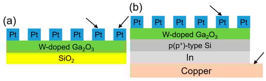
Figure 1.
Schematic diagrams of (a) the structure used for I-V measurements and (b) the structure used for I-V measurements of W-doped Ga2O3 thin films-p-type Si heterojunction diode. Arrows indicate the measurement contact points.
The fabrication process concluded with Pt top electrode deposition, creating the complete device structure, as Figure 1b illustrates, ready for current-voltage (I-V) characterization measurements. A comprehensive set of characterization techniques was employed to evaluate the properties of the W-doped Ga2O3 thin films. Field emission scanning electron microscopy (FESEM) was used to observe the surface morphology and determine W-doped Ga2O3 thin films’ thickness. When combined with Energy-Dispersive X-ray Spectroscopy (EDS), FESEM also enabled elemental quantitative analysis, confirming the successful incorporation of W into the Ga2O3 matrix. X-ray diffraction (XRD) was performed to identify the crystalline phases present in the films. In addition, UV–Vis spectroscopy was used to determine the optical bandgap by analyzing the transmission spectra, with measurements carried out on films deposited on transparent sapphire substrates. Elemental quantitative analysis and depth profiling was also conducted by using X-ray photoelectron spectroscopy (XPS) to analyze the distribution of these elements throughout the W-doped Ga2O3 thin films’ thickness.
XPS measurements were performed using a PHI VersaProbe 4 (Physical Electronics, Chanhassen, MN, USA) equipped with a monochromatic Al Kα X-ray source (1486.6 eV). Sample regions of interest were identified and aligned using the scanning X-ray imaging (SXI) mode, and the system’s ion gun (500 eV–5 keV monatomic Ar+) was available for sputtering. Survey spectra were acquired at a pass energy of ~93 eV with a step size of 0.5–1 eV, while high-resolution core-level spectra were recorded at a pass energy of ~23.5 eV with a step size of 0.05–0.1 eV. Multiple scans (typically 3–10 accumulations) were accumulated to improve the signal-to-noise ratio. Electrical characterization included current–voltage (I-V) measurements using an Agilent B1500A analyzer (Keysight Technologies, Santa Rosa, CA, USA) over a voltage range of −2 V to 2 V, generating I-V response curves. Furthermore, Hall effect equipment was used to determine key electrical parameters such as the carrier mobility, carrier concentration, and resistivity of the W-doped Ga2O3 thin films. As for the Hall measurements, they were performed using the van der Pauw configuration with indium contacts deposited at the four corners of the thin-film samples. A Hall measurement system (Lakeshore 7707, Lake Shore Cryotronics, Inc., Westerville, OH, USA) equipped with a calibrated electromagnet was employed. The carrier concentration, mobility, and resistivity were extracted under a magnetic field of ±0.55 T at room temperature.
3. Results and Discussion
Figure 2 examines the effect of WO3 doping on the microstructural characteristics of W-doped Ga2O3 thin films. As shown in the SEM surface image in Figure 2a, the surface morphology of the thin film is clearly observed. The image reveals that the surface of the W-doped Ga2O3 thin film is relatively smooth, with densely packed grains and no significant variation in grain size across the film. This uniform and compact morphology suggests that the WO3 doping process does not disrupt surface integrity but rather promotes a highly uniform film structure. According to the literature, tungsten doping is known to enhance the film’s density and surface uniformity [21,22]. This improvement is primarily attributed to the lower melting point of WO3 (~1473 °C) compared to that of Ga2O3 (~1900 °C). During the electron beam (E-beam) evaporation process, WO3 vaporizes earlier than Ga2O3, making it more likely to serve as a nucleation facilitator during film deposition. The early vaporization of WO3 generates a large number of nucleation sites, which contribute to the rapid and uniform formation of grains. These nucleation centers effectively suppress abnormal grain growth, resulting in a fine-grained and dense microstructure.
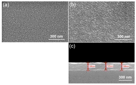
Figure 2.
SEM images of (a) the as-deposited un-doped and (b) W-doped Ga2O3 thin films and the surface (c) cross sessional W-doped Ga2O3 thin films.
This phenomenon is further supported by the depth-profile elemental analysis presented later in the study, which indirectly confirms that WO3 tends to vaporize prior to Ga2O3 during the deposition process. The elemental distribution data imply that the presence of WO3 in the early stages of deposition plays a crucial role in modifying the film’s nucleation dynamics and growth behavior. The formation of such a dense and uniform microstructure is particularly beneficial for applications requiring high-quality dielectric or semiconducting thin films. Furthermore, improved surface uniformity contributes to better interface characteristics when the film is integrated into device architectures. Therefore, WO3 doping not only improves the microstructural integrity of Ga2O3 thin films but also has potential implications for the performance and reliability of next-generation electronic and optoelectronic devices. Figure 2a illustrates the surface morphology of the as-deposited un-doped Ga2O3 thin films, which appear smooth and composed of densely packed particles. Nevertheless, noticeable cracks and voids are observed across the surface. These defects are commonly attributed to the nature of E-beam deposition, which can result in non-uniform film growth and localized structural discontinuities such as cracking or porosity.
In contrast, Figure 2b reveals a markedly different morphology for the as-deposited W-doped Ga2O3 thin films. The surface clearly exhibits the presence of microcrystalline structures, indicating that W doping induces partial crystallization within the otherwise amorphous matrix. This microstructural evolution reveals that tungsten incorporation plays a significant role in modifying the nucleation and growth dynamics during deposition, potentially enhancing the film’s structural integrity and altering its physical properties. Notably, no cracks or pores are observed on the film surface, suggesting that the film maintains good structural integrity and compactness. The absence of such defects is advantageous, as it contributes to improved mechanical stability and minimizes potential pathways for leakage currents in electronic applications. This also reflects the high quality of the deposition process and the beneficial role of WO3 doping in promoting a uniform and defect-free microstructure. Figure 2c presents the cross-sectional view of the W-doped Ga2O3 thin films. From the image, the film thickness is estimated to be approximately 200 nm. The cross-sectional morphology reveals that the film exhibits excellent thickness uniformity across the entire area, indicating a highly controlled and stable deposition process. This level of uniformity not only reflects the consistency of the E-beam evaporation parameters but also demonstrates the reliability of the process in producing films with well-defined and reproducible thicknesses. Such uniformity is essential for ensuring predictable electrical and optical behavior in device applications, where film thickness plays a critical role in performance.
Figure 3a shows the EDS mapping regions selected for compositional analysis of the W-doped Ga2O3 thin films, including a small area (yellow rectangle) and a larger area (green rectangle). These mappings were performed to verify the uniform distribution of different elements throughout the deposited films. The corresponding EDS spectra, shown in Figure 3b, clearly identify the presence of Ga, O, and W in the as-deposited films, confirming the successful incorporation of tungsten species. Quantitatively, the average atomic ratio of Ga, O, and W in the yellow-square area scan was 34.0:62.4:3.6, which closely matches the nominal target composition of 34.6:62.4:4.0. Notably, these values indicate that the Ga:O ratio deviated from the theoretical 2:3 stoichiometry of Ga2O3 and that there is a relatively lower W content. Using an accelerating voltage of 10 keV for EDS analysis allows the electron beam to penetrate beyond 200 nm into the sample. As a result, the measured composition predominantly reflects the W concentration across the entire thickness of the thin film. Furthermore, this deviation can be attributed to the introduction of WO3, which raises the oxygen content, thereby reducing the Ga:O ratio. When performing EDS analysis on thin film samples, the collected signal may include contributions not only from the film itself but also from the underlying layers or even the substrate. If the film thickness is insufficient, the resulting signal may be diluted by these contributions, leading to deviations in the measured elemental composition. In our case, the W-doped Ga2O3 thin films have a thickness of approximately 200 nm, which may not be sufficient to fully eliminate substrate influence, thereby introducing potential deviations in the quantified elemental ratios. These results collectively reinforce that WO3 is effectively incorporated into the Ga2O3 matrix, demonstrating the feasibility of the doping approach and its capability to tune the film composition in a controlled manner.
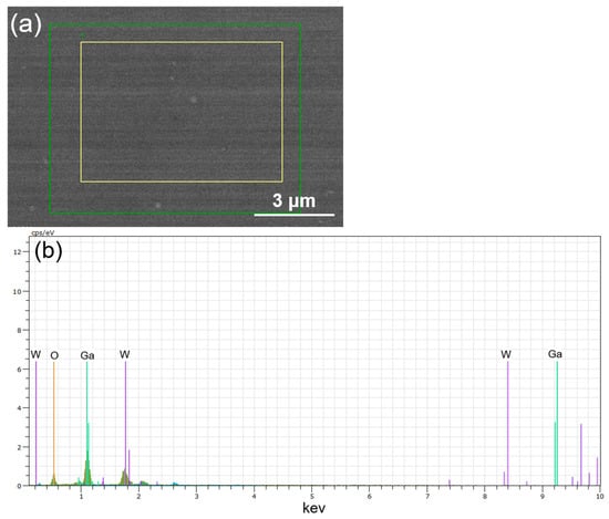
Figure 3.
EDS analysis of the W-doped Ga2O3 thin films: (a) two analysis areas (yellow and green) and (b) EDS spectra.
The XRD spectra provide insights into the crystalline properties of both un-doped and W-doped Ga2O3 thin films, with the diffraction peaks serving as indicators of potential structural and phase transformations. The results displayed in Figure 4 show that both the un-doped and W-doped Ga2O3 thin films predominantly exhibit an amorphous phase. For the un-doped Ga2O3 thin films, the XRD pattern displays a smooth and broad diffraction profile, characteristic of a fully amorphous structure [23]. In contrast, the W-doped Ga2O3 thin films exhibit irregular fluctuations in the diffraction spectrum. This difference can be attributed to the deposition dynamics during the E-beam evaporation process. In the case of un-doped Ga2O3, the evaporated material solidifies into a completely amorphous phase. However, for the W-doped Ga2O3 thin films, although the overall structure remains largely amorphous, the presence of WO3, which has a lower melting point than Ga2O3, can facilitate localized liquid-phase-assisted crystallization during film formation [24,25]. This process can promote the nucleation and growth of fine microcrystalline domains embedded within the amorphous matrix. As a result, the irregular fluctuations observed in the XRD pattern of the W-doped Ga2O3 thin films are likely caused by these undetectable or weakly diffracting crystalline phases, which are too small or too sparsely distributed to produce well-defined diffraction peaks but still perturb the amorphous background signal.
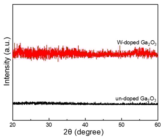
Figure 4.
XRD patterns of the un-doped and W-doped Ga2O3 thin films.
To further investigate the elemental composition of Ga, W, and O within the thin films, quantitative XPS analysis was performed, and the depth at which the XPS data were obtained, along with the original analysis spectrum, is presented in Figure 5a. The average atomic ratios of Ga (Ga2p3), O (O1s), and W (W4f) were determined to be 34.3:63.0:2.7. Notably, the relative concentration of W obtained from XPS was significantly lower than that measured via EDS. This discrepancy arises from the fundamental nature of XPS, because XPS is a highly surface-sensitive analytical technique. When used for elemental analysis, XPS primarily reflects the composition of the topmost surface layers of the material. This differs from depth profiling applications, where sputtering is employed to reveal subsurface information. Without sputtering, the measured elemental ratios predominantly represent the near-surface chemical composition, typically within a depth of 1–10 nm. As a result, it often fails to reflect the overall elemental distribution across the entire film thickness. This surface limitation of XPS becomes particularly relevant when considering the physical properties of the materials involved. According to previous SEM observations and known thermophysical characteristics, WO3 has a substantially lower melting point compared to Ga2O3. During the e-beam evaporation process, materials with lower melting points tend to vaporize and condense earlier than those with higher melting points. This suggests that WO3 likely undergoes preferential vaporization and subsequently deposits earlier at the film–substrate interface. Moreover, literature reports have shown that, at elevated substrate temperatures, the sticking coefficient of oxygen atoms on the substrate surface is lower than that of tungsten atoms [14].
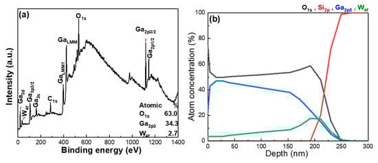
Figure 5.
(a) The original analysis spectrum and (b) the depth profile analysis of Ga, W, O, and Si elements of the W-doped Ga2O3 thin films.
This variation in surface adsorption behavior further suggests that fewer W atoms remain on the outermost surface layer of the thin film, which explains the lower W concentration detected by surface XPS measurements, and the analysis results for Ga, W, O, and Si elements are shown in Figure 5b. Based on this observation, it is reasonable to infer that the actual W doping concentration may be underestimated by surface-level XPS analysis. To validate this hypothesis and obtain a more complete picture of the W distribution throughout the film thickness, XPS depth-profile analysis was performed. This method enabled the investigation of the spatial distribution of W atoms under different doping conditions, as well as assessments of film uniformity and structural consistency. Figure 5b presents the atomic concentration profiles of Ga, W, O, and Si elements as a function of sputtering depth in the W-doped Ga2O3 thin films. The depth-resolved data reveal a clear gradient in W concentration: in the near-surface region (0–30 nm), the W concentration is relatively low. However, as the etching depth increases, the W concentration gradually rises, reaching its maximum near the film–substrate interface, around 200 nm. Beyond this depth, the W concentration slightly surpasses that of Ga in the same region. In contrast, the Ga concentration consistently decreases with increasing depth.
These findings strongly support the earlier hypothesis. The lower melting point of WO3 facilitates its early vaporization during deposition, allowing it to preferentially settle near the substrate interface. This results in a vertical compositional gradient, with W atoms becoming concentrated toward the bottom of the film. Importantly, the depth-profile results corroborate the surface XPS data and together offer a coherent explanation for the initially observed discrepancy in W content. The results confirm that conventional XPS primarily reflects surface composition and is insufficient for capturing the complete dopant distribution in the bulk of the film. The combination of surface XPS and depth-profile analyses reveals that W atoms exhibit a distinct decreasing trend in W atom concentration within the W-doped Ga2O3 thin films. This distinct decreasing trend is a direct consequence of the deposition dynamics governed by material properties such as the melting point and surface adhesion behavior. The findings highlight a crucial aspect of the WO3 doping strategy used in this study, namely, the tendency of W atoms to segregate toward the bottom of the film. This insight not only clarifies the limitations of surface analysis techniques but also underscores the importance of depth-resolved methods in accurately evaluating doping uniformity in thin-film systems.
Figure 6a presents the O1s spectra of W-doped Ga2O3 thin films. In general, the O1s peak can be deconvoluted into three nearly Gaussian components, denoted as OI, OII, and OIII. For the W-doped Ga2O3 thin films, the O1s peak was centered at 530.9 eV, and the peaks of OI, OII, and OIII were located at 530.1 ± 0.1 eV (OI), 530.9 ± 0.1 eV (OII), and 531.6 ± 0.1 eV (OIII). Such detailed analyses of the O1s spectra provide critical insights into the bonding characteristics of oxygen and their influence on the electronic and interfacial properties of the W-doped Ga2O3 thin films. The low binding energy peak (OI) is attributed to lattice oxygen (O2− in Ga–O), which reflects the presence of a well-ordered Ga2O3 crystal structure. The high binding energy peak (OIII) corresponds to surface-adsorbed oxygen species, such as OH−, H2O, and COx groups, which are typically associated with surface contamination or adsorption from the surrounding environment. In earlier studies, the medium binding energy peak (OII) was often attributed to oxygen vacancy–associated oxygen or defect-induced nonstoichiometric Ga2O3 states. Oxygen vacancies (Vo) have been widely regarded as the primary source of n-type conductivity in Ga2O3 thin films, since they can act as shallow donors and contribute free electrons to electrical transport [26].
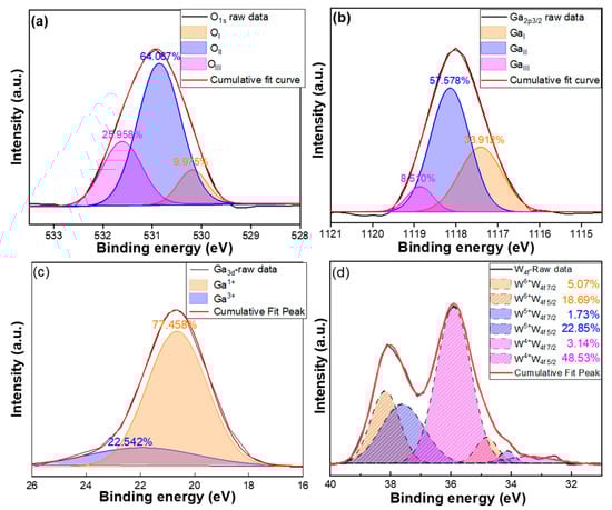
Figure 6.
XPS analysis spectra and the Gaussian-resolved components of the W-doped Ga2O3 thin films: (a) O1s spectrum, (b) Ga2p3/2 spectrum, (c) Ga3d spectrum, and (d) W4f spectrum.
However, H. Idriss has argued that this interpretation is incorrect and proposed that the OII component most likely originates from surface hydroxyls (dissociatively adsorbed water, ~531.3–531.5 eV), molecularly adsorbed water (~532.5–533 eV), and/or adventitious oxygen-containing contaminants [27]. As emphasized by Idriss, ex situ O1s signals in this energy range should not be taken as direct evidence of oxygen vacancies, since ambient exposure rapidly heals surface vacancies through water adsorption, and more reliable identification would require monitoring changes in the metal cation oxidation states or in situ/temperature-dependent measurements. Nevertheless, it should be noted that there is still no complete consensus in the literature, and many reports continue to interpret the OII component within the framework of oxygen-vacancy–related states. In this study, we follow this conventional approach to discuss our results. The OII component accounts for as much as 64.067% of the total O1s peak area, which suggests a relatively high concentration of donor-like defect states within the thin films. Such a pronounced proportion strongly supports the view that oxygen deficiency plays a critical role in enhancing the intrinsic n-type conductivity of Ga2O3 thin films and further indicates that the deposition conditions employed in this work effectively promote the formation of vacancy-related states favorable for carrier generation.
For the W-doped Ga2O3 thin films, the Ga2p3/2 spectrum can be deconvoluted into three distinct components, as Figure 6b shows. The first component, GaI, appearing at 1117.4 eV, is attributed to metallic bonding states such as Ga-Ga or Ga-W. The second component, GaII, located at 1118.1 eV, corresponds to the Ga2O3 lattice structure and represents gallium in its typical trivalent oxidation state. The third component, GaIII, observed at 1118.9 eV, is associated with Ga-O bonding environments or higher oxidation state gallium species present at the film surface or interface, such as Ga(OH)3 or hydrated oxides [28]. The relative intensities of these three components provide valuable insights into the chemical states of Ga, the degree of oxidation, and the surface chemistry of the W-doped Ga2O3 thin films. Among these, the low binding energy sub-peak GaI is widely regarded as a feature associated with oxygen vacancies, which play a crucial role in determining the electronic properties of Ga2O3. Since oxygen vacancies provide shallow donor states that release free electrons, GaI serves as the most direct spectral signature of enhanced n-type conductivity in Ga2O3. In this study, the GaI component accounts for 33.912% of the total Ga2p3/2 peak area, indicating a considerable concentration of vacancy-related states. This relatively high proportion strongly suggests that the W-doped Ga2O3 thin films possess abundant donor-like defects, which play a decisive role in boosting electron density and electrical transport. Compared with typical reports where GaI contributions are often lower, the observed value highlights the effectiveness of the deposition conditions in promoting oxygen vacancy formation and further demonstrates the potential of these films for applications in power electronics and devices requiring stable n-type conductivity.
The Ga3d spectrum of the W-doped Ga2O3 thin films can be deconvoluted into two distinct components: a Ga1+-related peak and a Ga-O bonding peak. The Ga1+ peak, located at the lower binding energy side, is generally attributed to oxygen vacancies or lattice defects, where Ga atoms exist in a partially reduced valence state, such as Ga2O [29]. According to the XPS reference data, metallic Ga exhibits characteristic binding energies at Ga2p3/2 and Ga3d (~18.8 eV), while Ga3+ does at ~20.3 eV of Ga3d. Therefore, if the GaI component observed in Ga2p3/2 were truly due to metallic Ga, a corresponding signal should also be present in the Ga3d core level. The absence of such a peak suggests that the assignment of GaI to metallic Ga may not be valid [30,31]. The pronounced Ga1+ component observed in the Ga3d spectrum indicates a highly reduced chemical environment, which is commonly associated with donor-like defects that can strongly influence the electrical conductivity, defect density, and carrier concentration of Ga2O3 thin films. In contrast, the higher binding energy peak corresponds to the conventional Ga-O bonding environment, where Ga predominantly exists in the Ga3+ state. While oxygen vacancies have often been proposed as one of the primary contributors to the intrinsic n-type conductivity of Ga2O3, it is important to note that such vacancies cannot be directly detected by XPS. Instead, the large proportion of Ga1+, accounting for as much as 77.458% of the total Ga3d peak area, suggests a significant presence of reduced Ga states that may be related to oxygen deficiency or other non-stoichiometric features. This substantial fraction implies that W-doping effectively promotes the formation of donor-like defect states, which are likely favorable for enhancing n-type conductivity and improving the suitability of Ga2O3 thin films for power electronics and next-generation semiconductor devices.
The W4f spectrum of the W-doped Ga2O3thin films was deconvoluted into contributions from W6+, W5+, and W4+ oxidation states. Each oxidation state was fitted as a spin–orbit doublet consisting of W4f7/2 and W4f5/2 peaks with a fixed area ratio of 4:3 and a spin–orbit splitting of ~2.1 eV, consistent with the degeneracy rule and standard XPS parameters for tungsten oxides. The highest binding energy doublet, assigned to W6+, corresponds to W6+-O bonding in WO3-like environments or substitutional W replacing Ga3+ in the Ga2O3 lattice. Such high-valence substitution acts as a shallow donor, since W6+ provides extra free electrons when occupying Ga3+ lattice sites, thereby serving as a direct contributor to n-type conductivity. The intermediate binding energy doublet, assigned to W5+, is commonly associated with oxygen-deficient environments and may also donate electrons to the conduction band, thus further enhancing conductivity. The lowest binding energy doublet, corresponding to W4+, reflects more strongly reduced W-O defect structures formed under highly reducing conditions, which may also contribute to donor-like behavior [32]. In this study, the W6+ component is clearly resolved, with the fitted W4f7/2 and W4f5/2 peaks accounting together for 23.76% of the total W4f peak area. This substantial proportion of W6+ indicates that a significant fraction of tungsten atoms substitute for Ga3+ in the lattice, effectively supplying a large number of donor electrons. These results strongly support the conclusion that W6+ substitution is a key mechanism driving the enhanced n-type conductivity observed in the W-doped Ga2O3 thin films.
In the past, various techniques have been used to calculate the optical bandgap (Eg) of different materials [1]. In this study, the Eg value was primarily determined using transmittance spectra data, analyzed via the Tauc plot method. This approach is based on the Tauc relation, which is commonly employed for estimating the optical bandgap of amorphous and crystalline semiconductors. The Tauc equation relates the absorption coefficient (α) and photon energy (hν) as follows:
where A is a constant, Eg is the optical bandgap, and n depends on the nature of the electronic transition (for direct allowed transitions, n = 2; for indirect allowed transitions, n = 1/2). As shown in Figure 7a, the variation in the bandgap energies is clearly observed. The calculated Eg value for the W-doped Ga2O3 thin films was 4.13 eV, which is noticeably higher than that of conventional amorphous Ga2O3 thin films. This significant increase in Eg can be attributed to the pre-sintering of the Ga2O3 powder at 950 °C, which partially transformed the material into the crystalline β-Ga2O3 phase prior to deposition. Although the as-deposited W-doped Ga2O3 thin films appear amorphous in nature, the elevated temperature during deposition, induced by the E-beam evaporation process, facilitated partial crystallization, particularly the formation of microcrystalline regions within the thin film.
(αhν)n = A (hν − Eg)
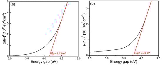
Figure 7.
Tauc plots of (a) the W-doped and (b) the undoped Ga2O3 thin films.
The presence of microcrystalline structures in the W-doped Ga2O3 thin films, as shown in Figure 1b, results from the deposition process using E-beam evaporation. During this process, the high-temperature melting, subsequent vaporization, and re-deposition cycles promote localized crystallization within the otherwise amorphous film. The microcrystal formation occurs due to the presence of WO3, which has a relatively low melting point compared to Ga2O3. During E-beam deposition, this lower melting point enhances atomic mobility, promoting local grain growth and crystallite formation even without a post-deposition annealing process. Moreover, the high thermal energy supplied by the E-beam activates residual β-Ga2O3 phase characteristics within the film. While the overall structure remains largely amorphous, localized regions exhibit β-phase-like behavior, contributing to the elevated Eg value. For comparison, Figure 7b shows the Eg calculation for undoped Ga2O3 thin films, which yielded an Eg of 3.78 eV. This value is significantly lower than the Eg of the W-doped Ga2O3 thin films, further supporting the conclusion that the increase in the bandgap is primarily a result of the E-beam-induced partial crystallization and the synergistic role of WO3 in enhancing crystallinity during deposition.
To enhance the electrical conductivity of as-deposited Ga2O3 thin films, which are inherently insulating, this study introduced WO3 as a dopant. As shown by the I-V measurements, the undoped Ga2O3 thin films exhibited negligible conductivity, making it nearly impossible to observe any meaningful I–V characteristics. Therefore, the corresponding I–V data for pure Ga2O3 thin films are not presented in this work. In contrast, the as-deposited W-doped Ga2O3 thin films demonstrated significantly improved electrical conductivity. Electrical characterization was performed using a Keysight B1500A semiconductor device analyzer, and the results are presented in Figure 8. Within the voltage range of −2 V to +2 V, the W-doped Ga2O3 thin films exhibited a clear conductive response, with the maximum current density reaching approximately 3 × 10⁻³ A/cm2. This result confirms that WO3 doping effectively enhances the electrical performance of Ga2O3 thin films, suggesting their potential for use in electronic device applications. Ga2O3 is generally known to exhibit n-type semiconducting behavior due to the presence of intrinsic defects or impurities that generate excess electrons within the bandgap. However, in practice, it is challenging for E-beam-deposited pure Ga2O3 thin films to display such n-type behavior; this result is caused by the limited defect formation or insufficient carrier activation under the deposition conditions.
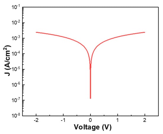
Figure 8.
Current–voltage curve of the W-doped Ga2O3 thin films.
In the case of W-doped Ga2O3 thin films, the enhanced n-type semiconducting characteristics are believed to arise from multiple contributing factors. WO3 itself is known to be an easily tunable semiconductor that can exhibit either n-type or p-type behavior depending on its stoichiometry and defect states [33]. The current–voltage characterization demonstrated that the as-deposited W-doped Ga2O3 thin films exhibit significantly enhanced electrical properties. To further investigate these properties, Hall effect measurements were conducted on the as-deposited W-doped Ga2O3 thin films. The results revealed a carrier mobility of 4.2 × 100 cm2/Vs, a carrier concentration of 2.135 × 10¹⁶/cm3, and a resistivity of 1.01 × 10² Ω·cm. Since the Hall coefficient exhibits a negative value, it indicates that the W-doped Ga2O3 thin films are n-type semiconductors. In contrast, the undoped Ga2O3 thin films showed negligible conductivity, rendering it impossible to accurately measure mobility and carrier concentration. These findings highlight the substantial improvement in electrical performance achieved through W doping.
The conductivity characteristics (current–voltage curve) and Hall parameters are significantly influenced by various factors such as the film thickness, doping concentration, material purity, and fabrication conditions employed during deposition. In this study, the incorporation of W into the Ga2O3 matrix could introduce donor states and increase the free electron concentration, thereby promoting n-type conduction in the resulting thin films. These parameters collectively govern the electrical behavior of W-doped Ga2O3 thin films, underscoring the inherent complexity in optimizing their conductivity for practical applications. WO3 can be readily incorporated into the Ga2O3 matrix during high-temperature deposition processes, primarily due to several favorable characteristics. First, WO3 has a notably lower melting point compared to Ga2O3, allowing it to exist in a molten-like state under deposition conditions, which promotes its interaction and integration with the host matrix. The enhanced conductivity of the W-doped Ga2O3 thin films can be attributed to the incorporation of W6+ ions, which increases the impurity concentration and effectively donates free carriers within the Ga2O3 matrix. Moreover, the high-temperature melting and deposition process inherent to E-beam evaporation facilitates the deeper and more uniform incorporation of WO3 into the Ga2O3 lattice, further amplifying these effects and resulting in the observed enhancement in conductivity.
Additionally, the ionic radius of W6+ (~0.060 nm) is close to that of Ga3+ (~0.062 nm), facilitating the effective substitution of Ga atoms within the Ga2O3 lattice. This similarity in ionic size minimizes lattice distortion and supports the structural incorporation of tungsten ions. WO3 is intrinsically an n-type semiconductor, and the W6+ dopants serve as donor ions, contributing free electrons to the system. When incorporated into Ga2O3, these electrons enhance the overall carrier concentration and improve the film’s electrical conductivity. Furthermore, the introduction of W6+ may alter the electronic band structure of Ga2O3, resulting in the formation of shallow donor levels or band tailing. Such modifications facilitate charge carrier generation and transport, thereby amplifying the n-type semiconducting behavior. In this study, we successfully transformed initially insulating Ga2O3 thin films into conductive W-doped Ga2O3 thin films through controlled WO3 doping. This transition highlights the effectiveness of our doping strategy and its significant impact on modifying the electrical properties of Ga2O3 thin films. The results demonstrate not only the feasibility of tuning conductivity via W incorporation but also the potential for employing such doped films in next-generation electronic and optoelectronic devices.
Figure 9 presents the I–V characteristics of heterojunction diodes formed by W-doped Ga2O3 thin films on p-type and p+-type Si substrates. Both device configurations exhibit pronounced rectifying behavior, indicating that the W-doped Ga2O3 thin films/p-Si structure possesses Schottky contact characteristics. The conduction mechanism is likely governed jointly by the potential barriers formed at both the metal–oxide and oxide–silicon interfaces. When the Si substrate is p-type, the forward turn-on voltage of the diode is approximately 5.5 V, with a maximum forward current density of about 0.10 mA/cm2 at an applied bias of 20 V. In reverse bias, the conduction is weak, with a maximum reverse current density of around 0.010 mA/cm2 at −20 V. When the substrate is changed to p+-type Si, the device exhibits a significantly lower forward turn-on voltage, indicating that it conducts more readily. The forward turn-on voltage decreases to approximately 2.5 V, after which the current rises sharply, reaching 1.0 mA/cm2 at around 3 V. In reverse bias, conduction becomes more pronounced: the diode begins conducting in reverse at approximately −3.6 V, and by −3.8 V, the reverse current reaches the instrument’s measurable limit of 1.0 mA/cm2.
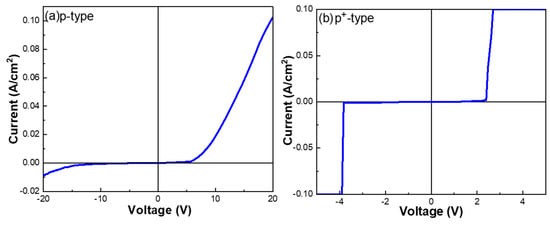
Figure 9.
The I–V characteristics of heterojunction diodes formed by W-doped Ga2O3 thin films on (a) p-type and (b) p+-type Si substrates.
The observed differences in the electrical characteristics between devices fabricated on p-type and p+-type Si substrates can be attributed to variations in the interfacial barrier properties. For the p-type Si substrate, a relatively higher barrier is formed at the Ga2O3/Si interface, requiring a larger forward bias (~5.5 V) to initiate conduction. As a result, the forward current density increases gradually, while the reverse leakage current remains relatively low. In contrast, the heavily doped p+-type Si substrate reduces the interfacial barrier height due to enhanced band bending and Fermi level alignment, thereby facilitating carrier injection or tunneling across the junction. This leads to a much lower forward turn-on voltage (~2.5 V) and significantly higher forward current. However, the reduced barrier also makes the junction more susceptible to reverse conduction, resulting in a pronounced increase in reverse leakage current, which becomes measurable at approximately −3.6 V. These results are consistent with the Hall effect measurements, which revealed an increase in the carrier concentration and conductivity with higher doping levels, confirming that an increased dopant concentration enhances carrier transport efficiency. Notably, the I-V curve of the p+-type Si sample exhibits a distinct current surge in the reverse bias region, a behavior reminiscent of a Zener diode. This phenomenon can be attributed to the following:
- (a)
- Barrierreduction and tunneling effect—The higher doping concentration in the p+-Si substrate lowers the potential barrier, concentrating the built-in electric field within the junction region. At a certain critical reverse bias, this facilitates electron tunneling (Zener tunneling) or defect-assisted conduction.
- (b)
- Depletion width compression—The high hole concentration in p+-Si produces a strong screening effect, further narrowing the depletion region and enabling the junction to enter reverse conduction more easily.
This reverse conduction behavior not only highlights the substantial impact of heavy doping on the band structure and junction electric field distribution but also suggests that such devices, when operated in a stable Zener region, hold potential for applications in overvoltage protection, voltage regulation circuits, and related device designs.
4. Conclusions
This study systematically investigated the structural, compositional, optical, and electrical properties of as-deposited un-doped and W-doped Ga2O3 thin films prepared via E-beam deposition. Surface morphology analysis revealed that un-doped Ga2O3 thin films exhibit smooth, densely packed particles but are interspersed with cracks and voids, defects commonly arising from the non-uniform growth inherent to E-beam processes. In contrast, W-doped Ga2O3 thin films displayed distinct microcrystalline features, indicating that tungsten incorporation induces partial crystallization within the otherwise amorphous matrix. EDS results confirmed that the atomic ratios of Ga, O, and W in both large-area and small-area scans closely match the nominal target composition, demonstrating high compositional fidelity in the deposition process. Complementary XPS analysis revealed a depth-dependent W distribution: near the surface, the W concentration is relatively low, gradually increasing with depth and reaching its peak near the film–substrate interface (~200 nm), where it slightly exceeds the Ga content. Conversely, the Ga concentration steadily decreases with increasing depth. Optical measurements indicated a noticeable bandgap widening with W doping. The W-doped Ga2O3 thin films exhibited an Eg of 4.132 eV, higher than that of the un-doped Ga2O3 thin films (3.784 eV) and the typical values reported for amorphous Ga2O3. This enhancement can be attributed to structural modification and local ordering effects induced by tungsten incorporation. The electrical characterization of the heterojunction diodes further highlighted the influence of substrate doping. For devices with p-type Si substrates, the forward turn-on voltage was ~5.5 V, with a maximum forward current density of ~0.10 mA/cm2 at 20 V and minimal reverse conduction (~0.010 mA/cm2 at −20 V). Substituting a p+-type Si substrate significantly improved forward conduction, reducing the turn-on voltage to ~2.5 V and yielding a rapid current increase to ~1.0 mA/cm2 at ~3 V. In reverse bias, conduction commenced at ~−3.6 V and quickly reached the measurement limit (~1.0 mA/cm2) at ~−3.8 V. Overall, the findings demonstrate that W doping effectively tailors the microstructure, enhances the optical bandgap, and influences the carrier transport properties of Ga2O3 thin films. Furthermore, the choice of substrate doping type plays a crucial role in determining heterojunction diode performance, offering a viable pathway for optimizing Ga2O3-based electronic and optoelectronic devices.
Author Contributions
Conceptualization, C.-T.L., Y.-W.W., C.-F.Y., and K.-W.M.; methodology, C.-T.L., Y.-W.W., C.-F.Y., and K.-W.M.; validation, C.-T.L., Y.-W.W., C.-F.Y., and K.-W.M.; formal analysis, C.-T.L., Y.-W.W., C.-F.Y., and K.-W.M.; investigation, C.-T.L., C.-F.Y., and K.-W.M.; data curation, C.-T.L., Y.-W.W., C.-F.Y., and K.-W.M.; writing—original draft preparation, C.-T.L., C.-F.Y., and K.-W.M.; writing—review and editing, C.-T.L., C.-F.Y., and K.-W.M.; visualization, C.-T.L., Y.-W.W., C.-F.Y., and K.-W.M. All authors have read and agreed to the published version of the manuscript.
Funding
The works are supported by Summit-Tech Resource Corp., by projects under Nos. NSTC 113-2622-E-390-001, NSTC 113-2221-E-390-011, and NSTC 113-2221-E-005-042, and by the funding of the Ministry of National Defense of Taiwan under the 2025 Military Instructor Research Grant.
Institutional Review Board Statement
Not applicable.
Informed Consent Statement
Not applicable.
Data Availability Statement
The original contributions presented in this study are included in the article. Further inquiries can be directed to the corresponding author.
Conflicts of Interest
Author Cheng-Fu Yang received research grants from Summit-Tech Resource Corp Company. The sponsors had no role in the design, execution, interpretation, or writing of the study.
References
- Lin, T.Y.; Han, S.Y.; Huang, C.Y.; Yang, C.F.; Wei, S. Using Different Methods to Measure the Optical Energy Bandgap of Un-annealed and Annealed Ga2O3 Films. Appl. Funct. Mater. 2021, 1, 25–30. [Google Scholar]
- Higashiwaki, M.; Sasaki, K.; Kuramata, A.; Masui, T.; Yamakoshi, S. Development of gallium oxide power devices. Phys. Status Solidi A 2013, 211, 21–26. [Google Scholar]
- Wang, C.; Yan, Q.; Zhang, C.; Su, C.; Zhang, K.; Sun, S. β-Ga2O3 Lateral Schottky Barrier Diodes with >10 kV Breakdown Voltage and Anode Engineering. IEEE Electron Device Lett. 2023, 44, 1684–1687. [Google Scholar] [CrossRef]
- Luo, X.; Hao, L.; Wei, Y.; Dai, K.; Peng, X.; Jiang, Z.; Wu, Y. High Breakdown Voltage β-Ga2O3 Schottky Barrier Diode with Fluorine-Implanted Termination. Microelectron. J. 2024, 150, 106269. [Google Scholar]
- Liu, Y.; He, T.; Wei, S. Study on Preparing β-Ga2O3 Films with Temperature-Controlled Buffer Layer by RF Magnetron Sputtering. Appl. Funct. Mater. 2022, 2, 24–29. [Google Scholar] [CrossRef]
- Girolami, M.; Bosi, M.; Pettinato, S.; Ferrari, C.; Lolli, R.; Seravalli, L.; Serpente, V.; Mastellone, M.; Trucchi, D.M.; Fornari, R. Structural and Photoelectronic Properties of κ-Ga2O3 Thin Films Grown on Polycrystalline Diamond Substrates. Materials 2024, 17, 519. [Google Scholar] [CrossRef] [PubMed]
- He, F.; Qin, Y.; Wang, Y.; Lin, Z.; Su, J.; Zhang, J.; Chang, J.; Hao, Y. Aqueous Solution Derived Amorphous Indium Doped Gallium Oxide Thin-Film Transistors. IEEE J. Electron Devices Soc. 2021, 9, 373–377. [Google Scholar] [CrossRef]
- Shen, Y.; Zhang, M.; He, S.; Bian, L.; Liu, J.; Chen, Z.; Xue, S.; Zhou, Y.; Yan, Y. Reliability Issues of Amorphous Oxide Semiconductor-Based Thin Film Transistors. J. Mater. Chem. C 2024, 12, 13707–13726. [Google Scholar] [CrossRef]
- Huang, C.-Y.; Wang, C.-Y.; Houng, M.-P.; Yang, C.-F.; Wang, N.-F.; Li, J.V. Enhancement of the Properties of a β-Ga2O3-Based Diode Using Fluorine-Doped Ga2O3 Films Deposited by a Liquid-Phase Method. Funct. Mater. Lett. 2021, 14, 2150050. [Google Scholar] [CrossRef]
- Varley, J.B.; Weber, J.R.; Janotti, A.; Van de Walle, C.G. Oxygen Vacancies and Donor Impurities in β-Ga2O3. Appl. Phys. Lett. 2010, 97, 142106. [Google Scholar] [CrossRef]
- Dong, L.; Jia, R.; Xin, B.; Peng, B.; Zhang, Y. Effects of Oxygen Vacancies on the Structural and Optical Properties of β-Ga2O3. Sci. Rep. 2017, 7, 40160. [Google Scholar] [CrossRef] [PubMed]
- Korhonen, E.; Tuomisto, F.; Gogova, D.; Wagner, G.; Baldini, M.; Galazka, Z.; Schewski, R.; Albrecht, M. Electrical Compensation by Ga Vacancies in Ga2O3 Thin Films. Appl. Phys. Lett. 2015, 10, 242103. [Google Scholar] [CrossRef]
- Bhandari, S.; Nardone, C.; Zvanut, M.E. Optical Transitions of Gallium Vacancies in Neutron Irradiated β-Ga2O3. J. Appl. Phys. 2022, 132, 025701. [Google Scholar] [CrossRef]
- Patel, K.J.; Panchal, C.J.; Kheraj, V.A.; Desai, M.S. Growth, Structural, Electrical and Optical Properties of the Thermally Evaporated Tungsten Trioxide (WO3) Thin Films. Mater. Chem. Phys. 2009, 114, 475–478. [Google Scholar] [CrossRef]
- Zade, V.; Mallesham, B.; Shantha-Kumar, S.; Bronson, A.; Ramana, C.V. Interplay between Solubility Limit, Structure, and Optical Properties of Tungsten-Doped Ga2O3 Compounds Synthesized by a Two-Step Calcination Process. Inorg. Chem. 2019, 58, 3707–3716. [Google Scholar] [CrossRef]
- Zade, V.; Mallesham, B.; Roy, S.; Shutthanandan, V.; Ramana, C.V. Electronic Structure of Tungsten-Doped β-Ga2O3 Compounds. ECS J. Solid State Sci. Technol. 2019, 8, Q3111–Q3115. [Google Scholar] [CrossRef]
- Mudiyanselage, D.H.; Da, B.; Adivarahan, J.; Wang, D.; He, Z.; Fu, K.; Zhao, Y.; Fu, H. β-Ga2O3-Based Heterostructures and Heterojunctions for Power Electronics: A Review of the Recent Advances. Electronics 2024, 13, 1234. [Google Scholar] [CrossRef]
- Wan, J.; Wang, H.; Zhang, C.; Li, Y.; Wang, C.; Cheng, H.; Li, J.; Ren, N.; Guo, Q.; Sheng, K. 3.3 kV-Class NiO/β-Ga2O3 Heterojunction Diode and Its Off-State Leakage Mechanism. Appl. Phys. Lett. 2024, 124, 243504. [Google Scholar] [CrossRef]
- Bokemeyer, P.; Petersen, C.; Dethloff, C.; Chen, Y.; von Wenckstern, H.; Grundmann, M.; Vogt, S. α-Ga2O3-Based Heterojunction Diodes and Junction Field-Effect Transistors. Phys. Status Solidi RRL 2025, 2400388. [Google Scholar] [CrossRef]
- Liao, C.-T.; Kao, C.-Y.; Su, Z.-T.; Lin, Y.-S.; Wang, Y.-W.; Yang, C.-F. Investigations of In2O3-Added SiC Semiconductive Thin Films and Manufacture of a Heterojunction Diode. Nanomaterials 2024, 14, 881. [Google Scholar] [CrossRef] [PubMed]
- Pan, G.; Yin, J.; Ji, K.; Li, X.; Cheng, X.; Jin, H.; Liu, J. Synthesis and Thermochromic Property Studies on W-Doped VO2 Films Fabricated by Sol-Gel Method. Sci. Rep. 2017, 7, 6132. [Google Scholar] [CrossRef]
- Sultana, R.; Islam, K.; Chakraborty, S. Tuning Optical and Electrochemical Properties of Nb2O5 Thin Films via WO3 Doping. Trans. Electr. Electron. Mater. 2025, 26, 48–59. [Google Scholar] [CrossRef]
- Li, S.; Yang, C.; Zhang, J.; Dong, L.; Cai, C.; Liang, H.; Liu, W. Tunable optical properties of amorphous-like Ga2O3 thin films deposited by electron-beam evaporation with varying oxygen partial pressures. Nanomaterials 2020, 10, 1760. [Google Scholar] [CrossRef] [PubMed]
- Favaretto, R.; Garcia, D.; Eiras, J.A. Effects of WO3 on the microstructure and optical transmittance of PLZT ferroelectric ceramics. J. Eur. Ceram. Soc. 2007, 27, 4037–4040. [Google Scholar] [CrossRef]
- Liu, X.; Zhao, M.; Gao, F.; Zhao, L.; Tian, C. Effects of WO3 additions on the phase structure and transition of zinc titanate ceramics. J. Alloys Compd. 2008, 450, 440–445. [Google Scholar] [CrossRef]
- Abenuz Acuña, J.R.; Perez, I.; Sosa, V.; Gamboa, F.; Elizalde, J.T.; Farías, R.; Carrillo, D.; Enríquez, J.L.; Burrola, A.; Mani, P. Sputtering power effects on the electrochromic properties of NiO films. Opt. Int. J. Light Electron Opt. 2021, 231, 166509. [Google Scholar] [CrossRef]
- Idriss, H. On the wrong assignment of the XPS O1s signal at 531–532 eV attributed to oxygen vacancies in photo- and electro-catalysts for water splitting and other materials applications. Surf. Sci. 2021, 712, 121894. [Google Scholar] [CrossRef]
- Correia, F.C.; Bundaleski, N.; Teodoro, O.M.N.D.; Correia, M.R.; Rebouta, L.; Mendes, A.; Tavares, C.J. XPS analysis of ZnO:Ga films deposited by magnetron sputtering: Substrate bias effect. Appl. Surf. Sci. 2018, 458, 1043–1049. [Google Scholar] [CrossRef]
- Cui, H.; Sai, Q.; Qi, H.; Zhao, J.; Si, J.; Pan, M. Analysis on the electronic trap of b-Ga2O3 single crystal. J. Mater. Sci. 2019, 54, 12643–12649. [Google Scholar] [CrossRef]
- Moulder, J.F.; Stickle, W.F.; Sobol, P.E.; Bomben, K.D. Handbook of X-Ray Photoelectron Spectroscopy; Perkin-Elmer Corporation: Eden Prairie, MN, USA, 1992. [Google Scholar]
- Wang, B.; Kobayashi, K.; Ishii, T.; Yamashita, H. Core-level electronic structure of gallium oxide and gallium nitride. J. Electron Spectrosc. Relat. Phenom. 2001, 114–116, 939–945. [Google Scholar]
- Sivakumar, R.; Gopalakrishnan, R.; Jayachandran, M.; Sanjeeviraja, C. Investigation of X-ray photoelectron spectroscopic (XPS), cyclic voltammetric analyses of WO3 films and their electrochromic response in FTO/WO3/electrolyte/FTO cells. Smart Mater. Struct. 2006, 15, 877. [Google Scholar] [CrossRef]
- Ganesan, K.; Ajikumar, P.K. Unusual Gas Sensor Response and Semiconductor-to-Insulator Transition in WO3-x Nanostructures: The Role of Oxygen Vacancy. Surf. Interfaces 2025, 65, 106433. [Google Scholar] [CrossRef]


Disclaimer/Publisher’s Note: The statements, opinions and data contained in all publications are solely those of the individual author(s) and contributor(s) and not of MDPI and/or the editor(s). MDPI and/or the editor(s) disclaim responsibility for any injury to people or property resulting from any ideas, methods, instructions or products referred to in the content. |
© 2025 by the authors. Licensee MDPI, Basel, Switzerland. This article is an open access article distributed under the terms and conditions of the Creative Commons Attribution (CC BY) license (https://creativecommons.org/licenses/by/4.0/).