
Temperature and Ambient Band Structure Changes in SnO2 for the Optimization of Hydrogen Response

 ,
,  ,
,  ,
, 
Abstract
1. Introduction
2. Results
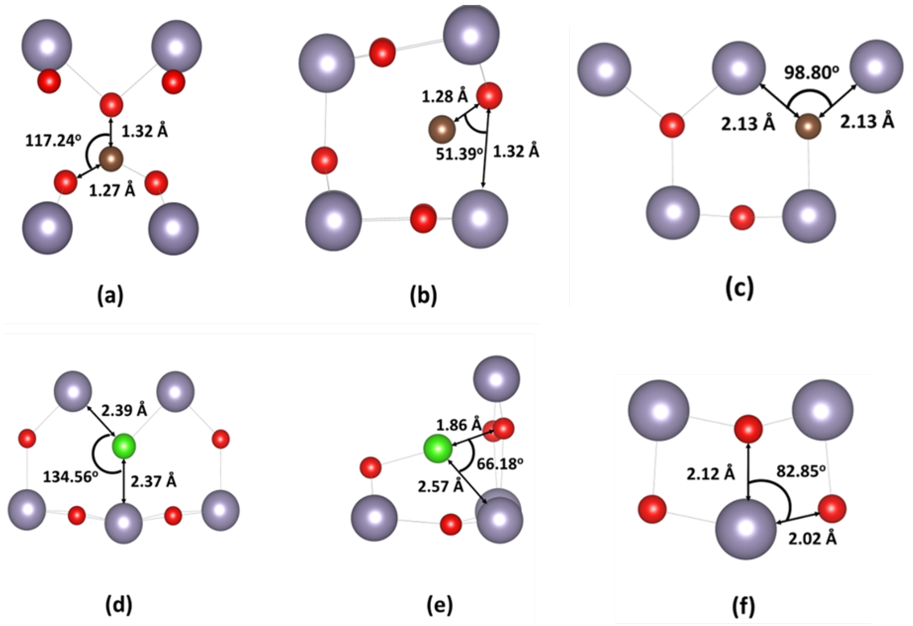
2.1. Theoretical
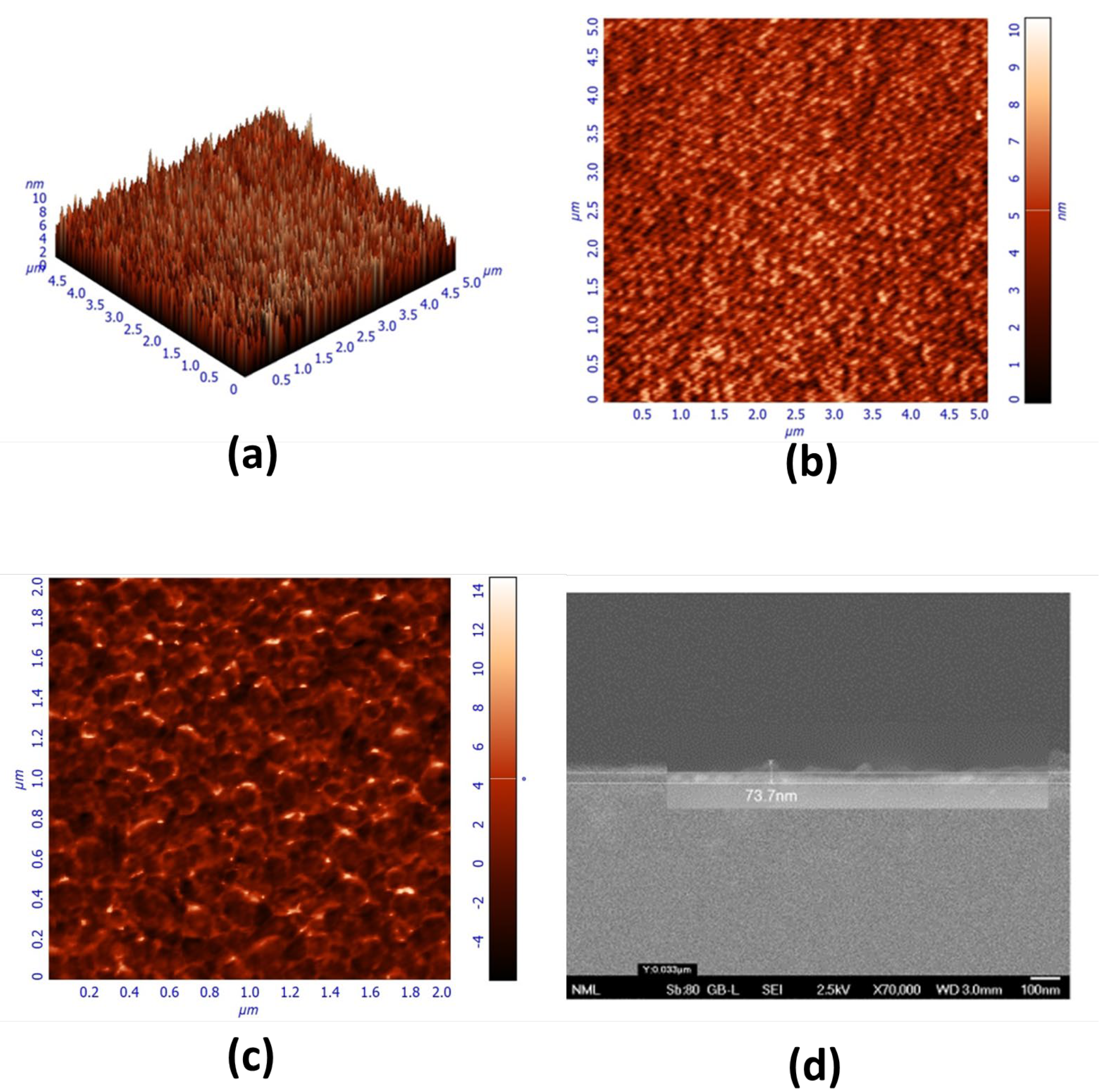
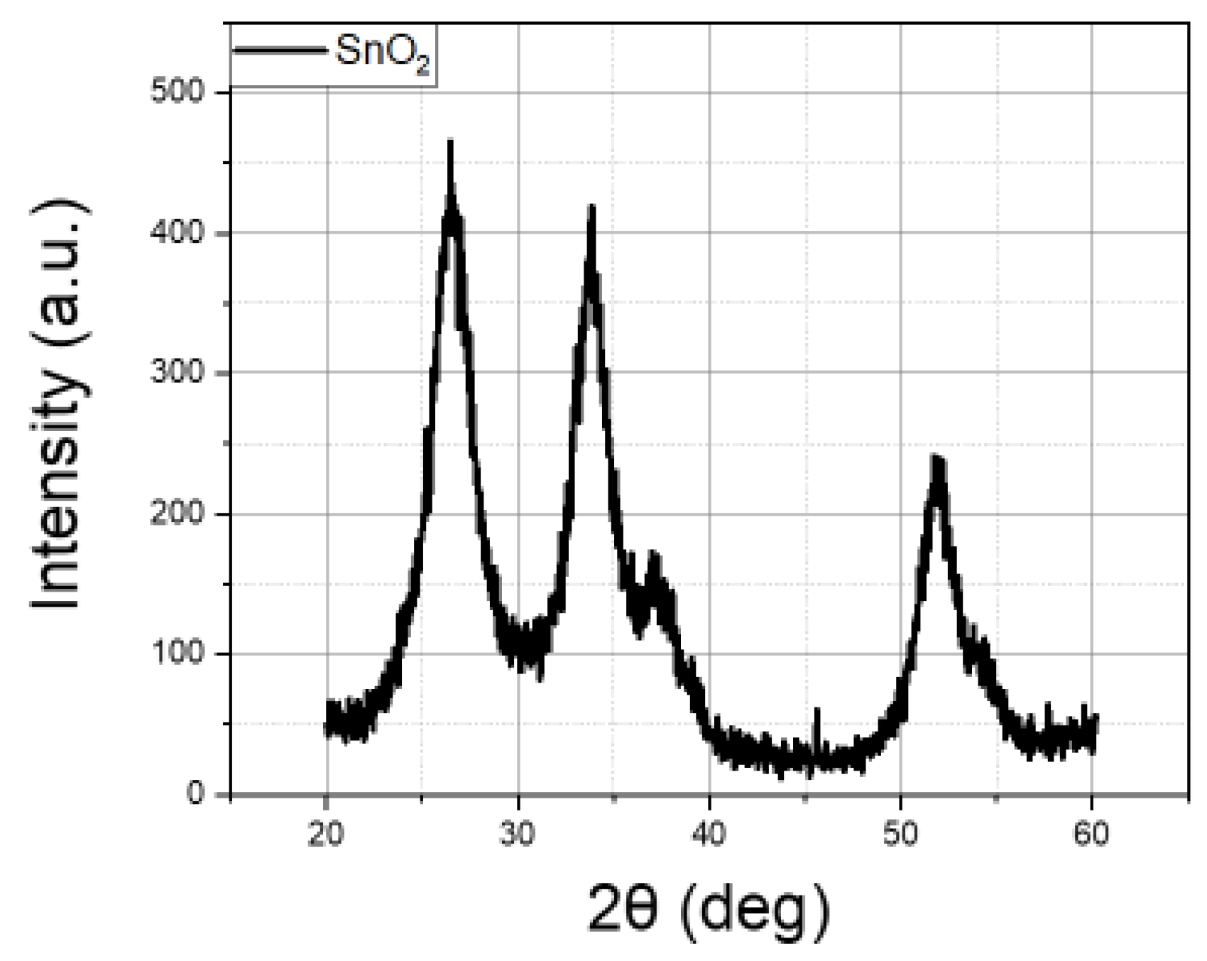
2.2. Structural Characterization
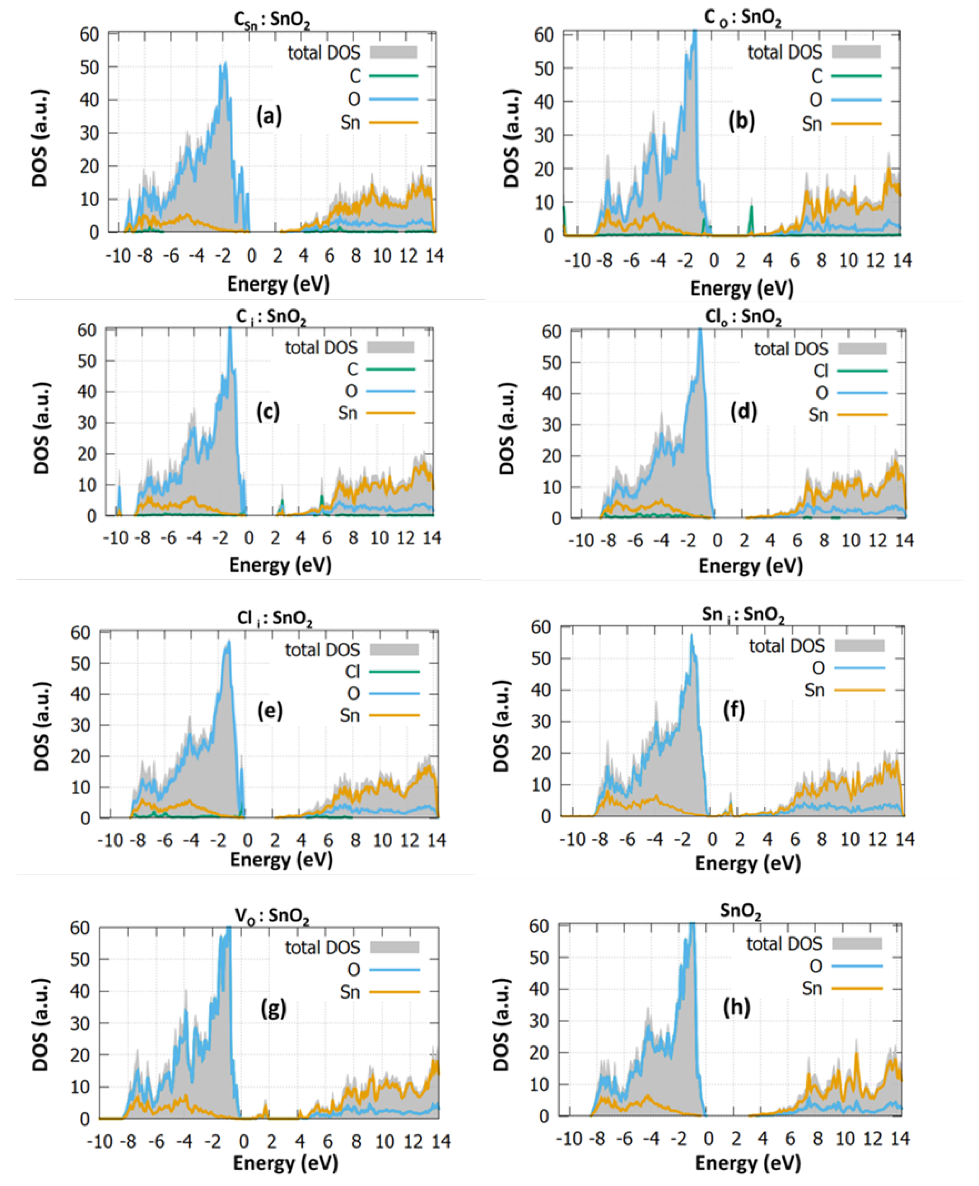
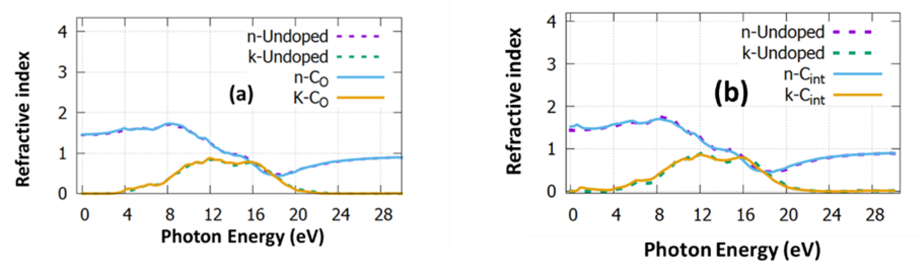
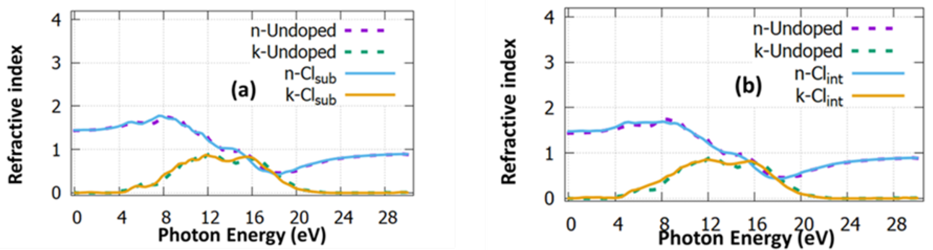
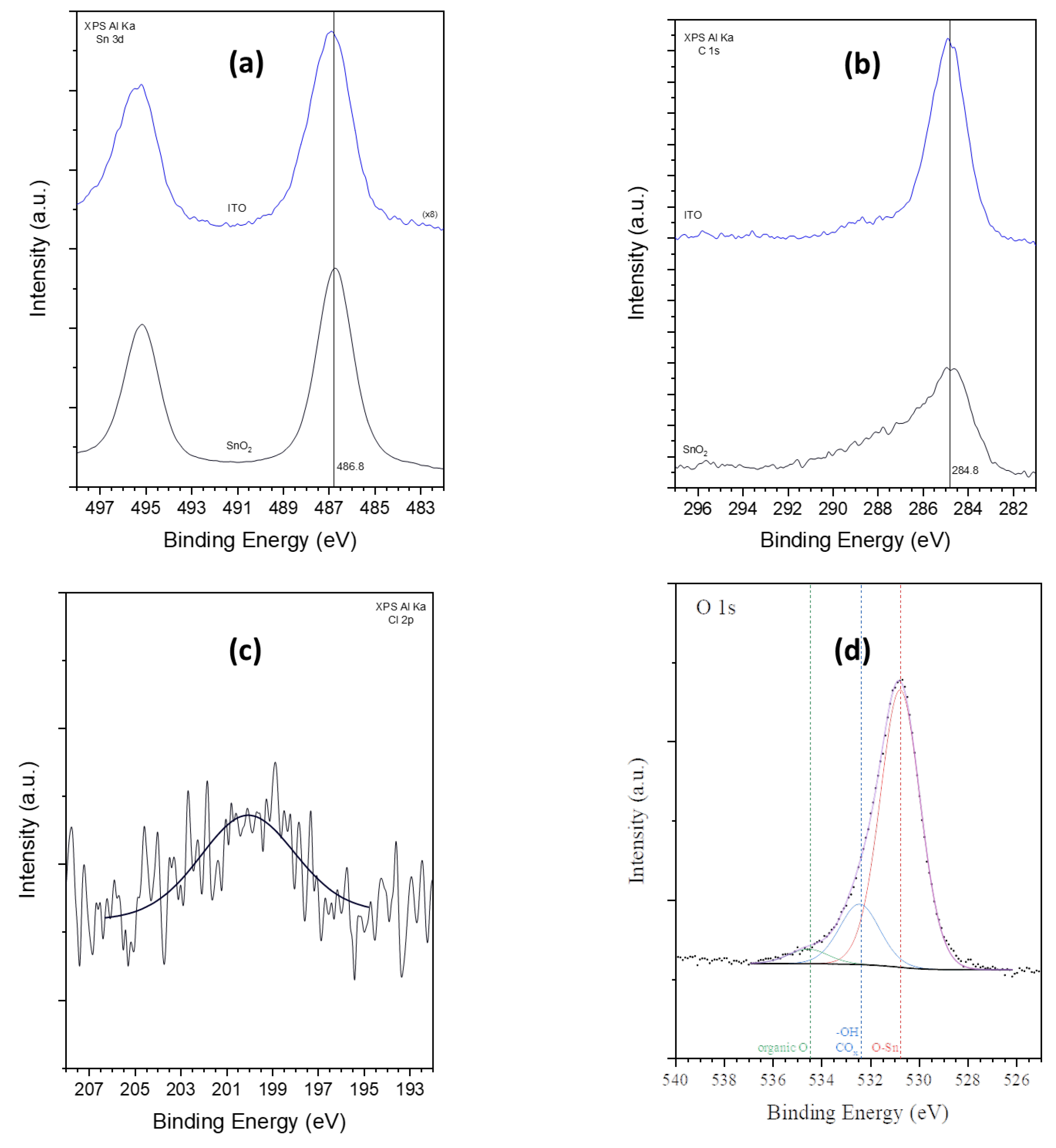
2.3. Electronic Characterization
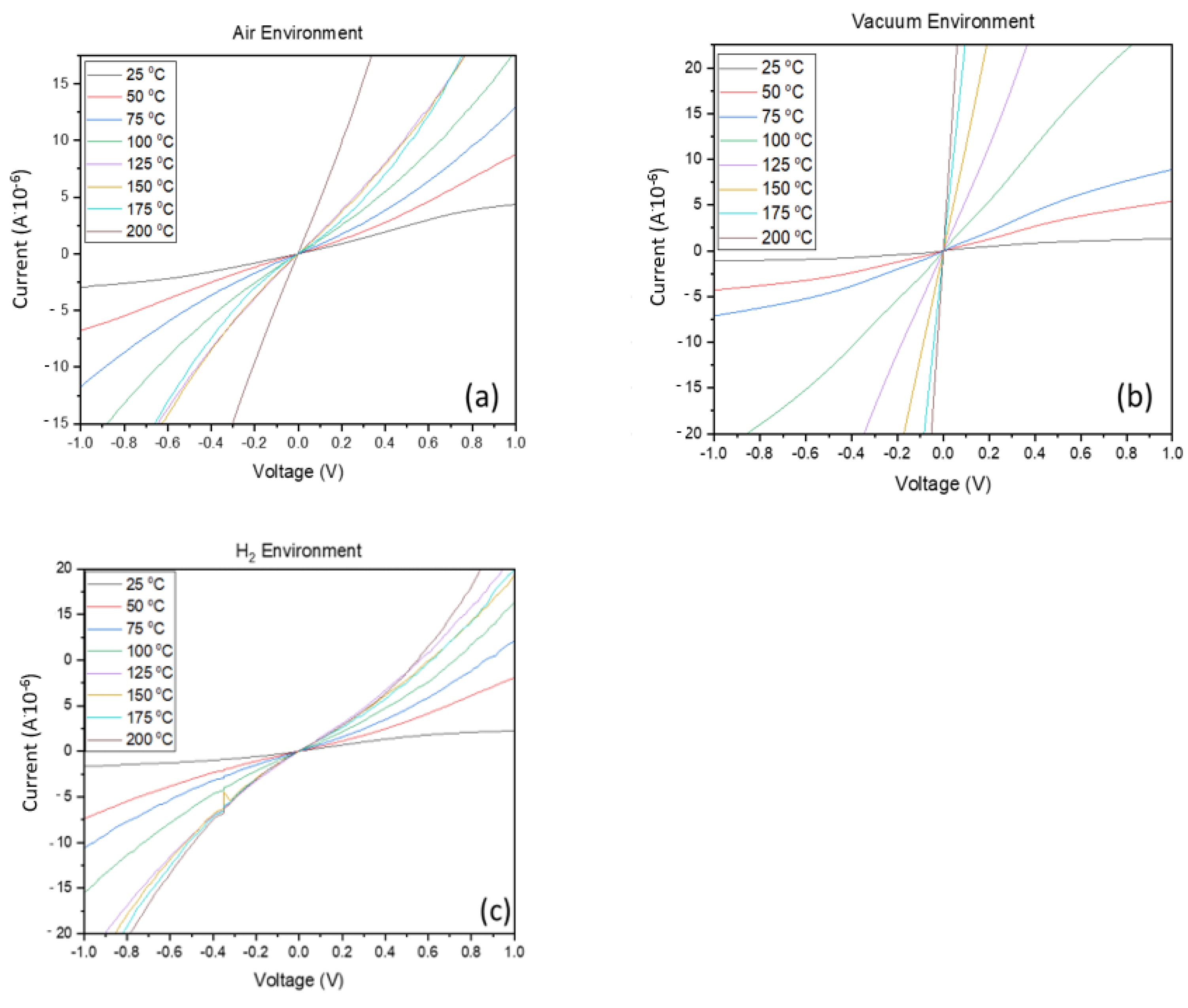
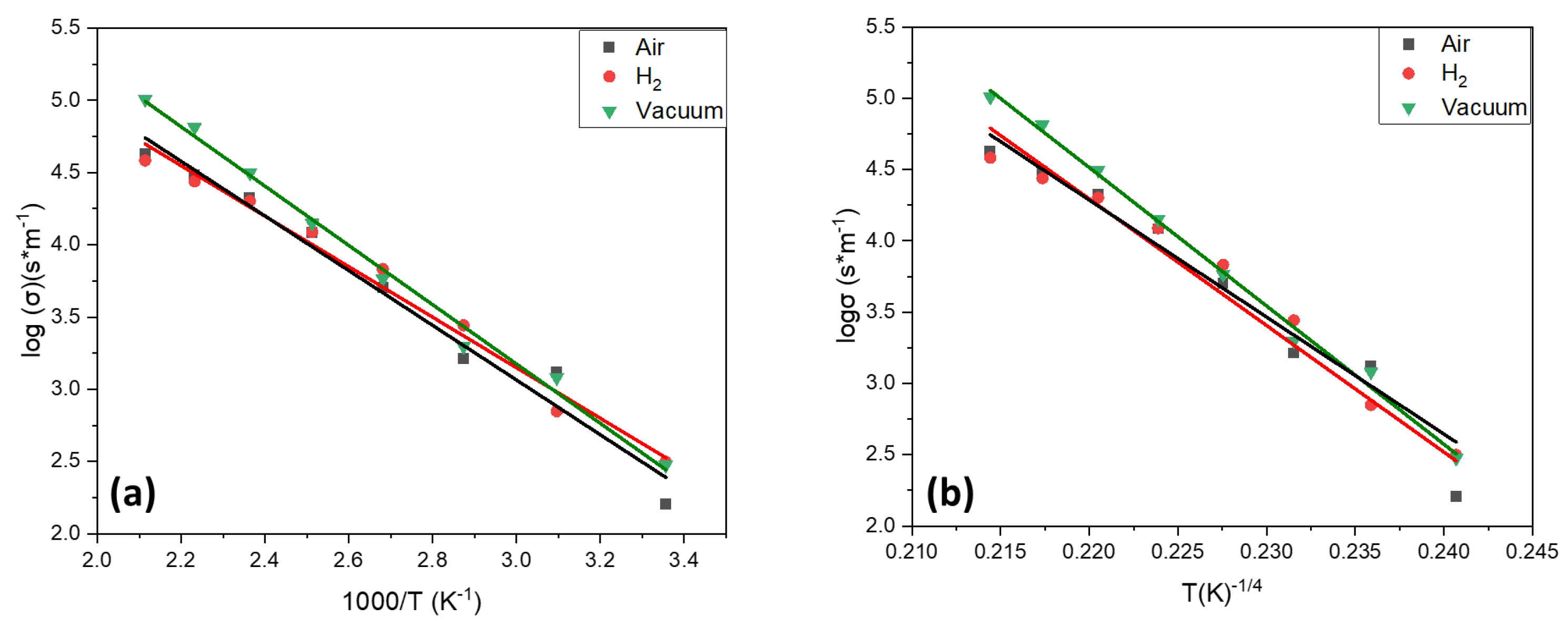
2.4. Electrical Characterization
3. Materials and Methods
4. Conclusions
Author Contributions
Funding
Institutional Review Board Statement
Informed Consent Statement
Data Availability Statement
Acknowledgments
Conflicts of Interest
References
- Heilig, A.; Bârsan, N.; Weimar, U.; Schweizer-Berberich, M.; Gardner, J.; Göpel, W. Gas identification by modulating temperatures of SnO2-based thick film sensors. Sens. Actuators B Chem. 1997, 43, 45–51. [Google Scholar] [CrossRef]
- Lee, S.H.; Hoffman, D.M.; Jacobson, A.J.; Lee, T.R. Transparent, Homogeneous Tin Oxide (SnO2) Thin Films Containing SnO2-Coated Gold Nanoparticles. Chem. Mater. 2013, 25, 4697–4702. [Google Scholar] [CrossRef]
- Dai, Z.R.; Pan, Z.W.; Wang, Z.L. Growth and Structure Evolution of Novel Tin Oxide Diskettes. J. Am. Chem. Soc. 2002, 124, 8673–8680. [Google Scholar] [CrossRef]
- Batzill, M.; Diebold, U. The surface and materials science of tin oxide. Prog. Surf. Sci. 2005, 79, 47–154. [Google Scholar] [CrossRef]
- Ghoshtagore, R.N. Mechanism of CVD Thin Film SnO2 Formation. J. Electrochem. Soc. 1978, 125, 110–117. [Google Scholar] [CrossRef]
- Wang, H.; Rogach, A.L. Hierarchical SnO2 Nanostructures: Recent Advances in Design, Synthesis, and Applications. Chem. Mater. 2014, 26, 123–133. [Google Scholar] [CrossRef]
- Takenaka, S.; Takahashi, R.; Sato, S.; Sodesawa, T.; Matsumoto, F.; Yoshida, S. Pore size control of mesoporous SnO2 prepared by using stearic acid. Microporous Mesoporous Mater. 2003, 59, 123–131. [Google Scholar] [CrossRef]
- Xu, C.; Tamaki, J.; Miura, N.; Yamazoe, N. Grain size effects on gas sensitivity of porous SnO2-based elements. Sens. Actuators B Chem. 1991, 3, 147–155. [Google Scholar] [CrossRef]
- Ponce, M.A.; Aldao, C.M.; Castro, M.S. Influence of particle size on the conductance of SnO2 thick films. J. Eur. Ceram. Soc. 2003, 23, 2105–2111. [Google Scholar] [CrossRef]
- Messad, A.; Bruneaux, J.; Cachet, H.; Froment, M. Analysis of the effects of substrate temperature, concentration of tin chloride and nature of dopants on the structural and electrical properties of sprayed SnO2 films. J. Mater. Sci. 1994, 29, 5095–5103. [Google Scholar] [CrossRef]
- Volintiru, I.; de Graaf, A.; van Deelen, J.; Poodt, P. The influence of methanol addition during the film growth of SnO2 by atmospheric pressure chemical vapor deposition. Thin Solid Films 2011, 519, 6258–6263. [Google Scholar] [CrossRef]
- Petaroudis, C.; Kostis, I.; Filippatos, P.-P.; Chroneos, A.; Soultati, A.; Vasilopoulou, M.; Davazoglou, D. Influence of thermal cycling on the optical and the electrical properties of atmospheric pressure chemical vapor deposited tin oxide films grown using water and methanol vapors as oxidizers. Thin Solid Films 2021, 734, 138841. [Google Scholar] [CrossRef]
- Lu, P.-F.; Shen, Y.; Yu, Z.-Y.; Zhao, L.; Li, Q.-Y.; Ma, S.-J.; Han, L.-H.; Liu, Y.-M. Electronic Structure and Optical Properties of Antimony-Doped SnO2 from First-Principle Study. Commun. Theor. Phys. 2012, 57, 145–150. [Google Scholar] [CrossRef]
- Filippatos, P.-P.; Kelaidis, N.; Vasilopoulou, M.; Davazoglou, D.; Chroneos, A. Defect Processes in Halogen Doped SnO2. Appl. Sci. 2021, 11, 551. [Google Scholar] [CrossRef]
- Hoa Hong, N.; Song, J.-H.; Raghavender, A.T.; Asaeda, T.; Kurisu, M. Ferromagnetism in C-doped SnO2 thin films. Appl. Phys. Lett. 2011, 99, 052505. [Google Scholar] [CrossRef]
- Zervos, M.; Lathiotakis, N.; Kelaidis, N.; Othonos, A.; Tanasae, E.; Vasilee, E. Epitaxial highly ordered Sb:SnO2 nanowires grown by the vapor liquid solid mechanism on m-, r- and a-Al2 O3. Nanoscale Adv. 2019, 1, 1980–1990. [Google Scholar] [CrossRef]
- Filippatos, P.-P.; Kelaidis, N.; Vasilopoulou, M.; Davazoglou, D.; Chroneos, A. Atomic structure and electronic properties of hydrogenated X (=C, Si, Ge, and Sn) doped TiO2: A theoretical perspective. AIP Adv. 2020, 10, 115316. [Google Scholar] [CrossRef]
- Brousse, T.; Schleich, D.M. Sprayed and thermally evaporated SnO2 thin films for ethanol sensors. Sens. Actuators B Chem. 1996, 31, 77–79. [Google Scholar] [CrossRef]
- Ren, X.; Liu, Y.; Lee, D.G.; Kim, W.B.; Han, G.S.; Jung, H.S.; Liu, S. Chlorine-modified SnO2 electron transport layer for high-efficiency perovskite solar cells. InfoMat 2020, 2, 401–408. [Google Scholar] [CrossRef]
- Vincent, C.A. The Nature of Semiconductivity in Polycrystalline Tin Oxide. J. Electrochem. Soc. 1972, 119, 515. [Google Scholar] [CrossRef]
- Afify, H.H.; Momtaz, R.S.; Badawy, W.A.; Nasser, S.A. Some physical properties of fluorine-doped SnO2 films prepared by spray pyrolysis. J. Mater. Sci. Mater. Electron. 1991, 2, 40–45. [Google Scholar] [CrossRef]
- Yakuphanoglu, F. Electrical conductivity, Seebeck coefficient and optical properties of SnO2 film deposited on ITO by dip coating. J. Alloys Compd. 2009, 470, 55–59. [Google Scholar] [CrossRef]
- Filippatos, P.-P.; Kelaidis, N.; Vasilopoulou, M.; Davazoglou, D.; Lathiotakis, N.N.; Chroneos, A. Defect processes in F and Cl doped anatase TiO2. Sci. Rep. 2019, 9, 19970. [Google Scholar] [CrossRef] [PubMed]
- Rasheed, R.T.; Al-Algawi, S.D. Annealing Effect of SnO2 Nanoparticles Prepared by the Sol–Gel Method. J. Adv. Phys. 2016, 5, 236–240. [Google Scholar] [CrossRef]
- Lv, Y.; Han, C.; Zhu, Y.; Zhang, T.; Yao, S.; He, Z.; Dai, L.; Wang, L. Recent advances in metals and metal oxides as catalysts for vanadium redox flow battery: Properties, structures, and perspectives. J. Mater. Sci. Technol. 2021, 75, 96–109. [Google Scholar] [CrossRef]
- Filippatos, P.-P.; Sharma, R.; Soultati, A.; Kelaidis, N.; Petaroudis, C.; Alivisatou, A.-A.; Drivas, C.; Kennou, S.; Christopoulos, S.-R.G.; Davazoglou, D.; et al. Optimization of the hydrogen response characteristics of halogen-doped SnO2. Sci. Rep. 2023, 13, 2524. [Google Scholar] [CrossRef] [PubMed]
- Myong, S.Y.; Lim, K.S. Universal single-phonon variable range hopping conduction for inorganic semiconducting polycrystalline films. Appl. Phys. Lett. 2006, 88, 222110. [Google Scholar] [CrossRef]
- Mott, N.F. Conduction in glasses containing transition metal ions. J. Non-Cryst. Solids 1968, 1, 1–17. [Google Scholar] [CrossRef]
- Plugaru, R.; Sandu, T.; Plugaru, N. First principles study and variable range hopping conductivity in disordered Al/Ti/Mn-doped ZnO. Results Phys. 2012, 2, 190–197. [Google Scholar] [CrossRef]
- Segall, M.D.; Lindan, P.J.D.; Probert, M.J.; Pickard, C.J.; Hasnip, P.J.; Clark, S.J.; Payne, M.C. First-principles simulation: Ideas, illustrations and the CASTEP code. J. Phys. Condens. Matter 2002, 14, 2717–2744. [Google Scholar] [CrossRef]
- Perdew, J.P.; Burke, K.; Ernzerhof, M. Generalized Gradient Approximation Made Simple. Phys. Rev. Lett. 1996, 77, 3865–3868. [Google Scholar] [CrossRef] [PubMed]
- Paier, J.; Marsman, M.; Hummer, K.; Kresse, G.; Gerber, I.; Ángyán, J.G. Screened hybrid density functionals applied to solids. J. Chem. Phys. 2006, 124, 154709. [Google Scholar] [CrossRef] [PubMed]


| SnO2 | |
|---|---|
| Sn | 1.0 |
| O | 1.94 |
| Cl | 0.02 |
| Chemical Environment | Activation Energy (eV) ± 0.05 eV |
|---|---|
| Dry Air | 0.37 |
| Vacuum | 0.40 |
| H2 | 0.34 |
Disclaimer/Publisher’s Note: The statements, opinions and data contained in all publications are solely those of the individual author(s) and contributor(s) and not of MDPI and/or the editor(s). MDPI and/or the editor(s) disclaim responsibility for any injury to people or property resulting from any ideas, methods, instructions or products referred to in the content. |
© 2023 by the authors. Licensee MDPI, Basel, Switzerland. This article is an open access article distributed under the terms and conditions of the Creative Commons Attribution (CC BY) license (https://creativecommons.org/licenses/by/4.0/).
Share and Cite
Filippatos, P.-P.; Soultati, A.; Kelaidis, N.; Davazoglou, D.; Vasilopoulou, M.; Drivas, C.; Kennou, S.; Chroneos, A. Temperature and Ambient Band Structure Changes in SnO2 for the Optimization of Hydrogen Response. Inorganics 2023, 11, 96. https://doi.org/10.3390/inorganics11030096
Filippatos P-P, Soultati A, Kelaidis N, Davazoglou D, Vasilopoulou M, Drivas C, Kennou S, Chroneos A. Temperature and Ambient Band Structure Changes in SnO2 for the Optimization of Hydrogen Response. Inorganics. 2023; 11(3):96. https://doi.org/10.3390/inorganics11030096
Chicago/Turabian StyleFilippatos, Petros-Panagis, Anastasia Soultati, Nikolaos Kelaidis, Dimitris Davazoglou, Maria Vasilopoulou, Charalampos Drivas, Stella Kennou, and Alexander Chroneos. 2023. "Temperature and Ambient Band Structure Changes in SnO2 for the Optimization of Hydrogen Response" Inorganics 11, no. 3: 96. https://doi.org/10.3390/inorganics11030096
APA StyleFilippatos, P.-P., Soultati, A., Kelaidis, N., Davazoglou, D., Vasilopoulou, M., Drivas, C., Kennou, S., & Chroneos, A. (2023). Temperature and Ambient Band Structure Changes in SnO2 for the Optimization of Hydrogen Response. Inorganics, 11(3), 96. https://doi.org/10.3390/inorganics11030096