Article

Investigation of Photoelectrochemical Performance under the Piezoelectric Effect Based on Different Zinc Oxide Morphologies

1
College of Science, Hubei University of Technology, Wuhan 430068, China
2
School of Materials Science and Engineering & Tianjin Key Laboratory of Building Green Functional Materials, Tianjin Chengjian University, Tianjin 300384, China
*
Author to whom correspondence should be addressed.
Inorganics 2023, 11(1), 11; https://doi.org/10.3390/inorganics11010011
Submission received: 16 November 2022 / Revised: 9 December 2022 / Accepted: 22 December 2022 / Published: 26 December 2022
(This article belongs to the Special Issue Photoelectrodes for Water Splitting)

Abstract

:
Recently, the piezoelectric effect has been widely used in photoelectrochemical (PEC) water splitting, and the morphology of the piezoelectric material is a critical factor affecting the piezo-photoelectrochemical water splitting performance. Herein, we explored the mechanism of the piezo-photoelectrochemical performance of zinc oxide (ZnO) that is affected by the morphology. Firstly, three different ZnO nanostructures (nanosheets, nanorods, and nanospheres) were synthesized by the electrodeposition, hydrothermal, and sol-gel methods, respectively. Then, the measurements of PEC water splitting performance under the piezoelectric effect revealed a 3-fold increase for the ZnO nanosheets, a 1.4-fold increase for the nanorods, and a 1.2-fold increase for the nanospheres compared to no piezoelectric effect. Finally, finite element simulation showed that nanosheets generated the highest piezoelectric potential (0.6 V), followed by nanorods (0.2 V), and nanospheres the lowest (0.04 V). Thus, among the three morphologies, the ZnO nanosheets exhibited a great improvement in PEC performance under the piezoelectric effect. The great improvement is due to the non-axial vertical homogeneous growth of the ZnO nanosheets, subjecting them to the highest effective deformation stress, which enables the ZnO nanosheets to produce the highest piezoelectric potential to accelerate the carrier separation and limit the recombination of photoelectrons and holes. This work serves as a guide for developing various photoelectrodes that are used in piezo-photoelectrochemical water splitting.

1. Introduction

Environmental pollution and energy crises will result from the use of toxic fossil fuels throughout societal development and the steady depletion of global fossil fuel reserves [1,2,3]. Therefore, it is crucial to develop a clean energy source. Hydrogen (H2) energy is typically considered unpolluted because water is the only byproduct of hydrogen combustion. However, conventional hydrogen generation is an expensive and energy-intensive process. Therefore, it is crucial to discover a low-energy and low-cost technique for hydrogen synthesis. Photoelectrochemical (PEC) water splitting [4] has started gaining popularity among researchers since Fujishima and Honda used TiO2 as an electrode to transform solar energy into the molecular energy of H2 and O2 in 1972 [5]. Since then, various semiconductors have become common research subjects in PEC water splitting. These semiconductors are classified as either n-type or p-type, depending on whether electrons or holes are the predominant conductors. n-type semiconductors conduct electricity mainly by electrons, such as WO3 [6], BiVO4 [7], TiO2 [8], and α-Fe2O3 [9]. In comparison, p-type semiconductors conduct electricity mainly by holes, such as Cu2O [10], CuO [11], BiOI [12], and CuBi2O4 [13]. However, various factors limit the efficiency of PEC water splitting. Among these factors, two main factors are the low utilization of light and the rapid recombination of photoelectrons and holes [14,15,16]. To solve these two major problems, researchers have proposed various semiconductor modification approaches, such as heterojunctions [17], surface plasmon resonance (SPR) effects [18], and doping [19]. Specifically, Zhang et al. fabricated a Cu2O/g-C3N4 heterojunction electrode successfully. Under external bias voltage of −0.4 V and visible light irradiation, the photocurrent density and PEC hydrogen evolution efficiency were −1.38 mA/cm2 and 0.48 mL/(h·cm2), respectively [20]. Li et al. fabricated a Pt/WO3/Ag photoanode by depositing Pt nanoparticles and Ag nanoparticles on the bottom and surface of WO3, respectively. The photocurrent of this photoanode was 1.13 mA/cm2 at 1.23 VRHE, which was 3.32 times higher than that of pure WO3 since the SPR effect of the Ag nanoparticles promotes charge separation [21].
In addition to the approaches that were mentioned above for modifying the properties of semiconductors, the piezoelectric effect has recently become a major research subject in PEC water splitting [22,23]. This is because the polarized electric field that is generated by the piezoelectric effect effectively accelerates the carrier separation within the material and suppresses the recombination of photoelectrons and holes, greatly enhancing the efficiency of PEC. In addition, the piezoelectric effect is easily achieved by deforming the material as it is stressed [24,25]. Consequently, researchers have focused on piezoelectric materials such as ZnO [26], NaNbO3 [27], CdS [28], and BaTiO3 [29]. ZnO possesses a high piezoelectric coefficient and mobility among these piezoelectric materials [30]. In addition, ZnO also possesses properties that are low cost, non-toxic, and easy to synthesize in different morphologies such as nanosheets [31], nanorods [32], and nanospheres [33]. Thus, ZnO has become popular for researchers investigating the piezoelectric effect on enhanced PEC water splitting. Specifically, Hong et al. used ultrasonic waves to develop strain-induced polarized charges on ZnO microfibers, demonstrating that the piezoelectric catalytic process of polarized ZnO is stable in triggering redox reactions [34]. Chen et al. synthesized Z-scheme ZnO-WO3−x nanoarrays for PEC water splitting via a hydrothermal method and demonstrated that piezoelectric coupled ZnO could enhance Z-scheme performance where the optimized photocurrent is 3.02 times higher than that of pure ZnO [35]. It is well known that the morphology of the piezoelectric material is an important factor in the piezoelectric effect. However, most studies have focused on the function of the piezoelectric effect in composite materials, and there needs to be more research into the influence of essential characteristics of zinc oxide on piezo-photoelectrochemical performance. Therefore, it is crucial to research a link between the morphology of ZnO and piezo-photoelectrochemical performance.
In this paper, we first explore the mechanism of piezo-photoelectrochemical performance that is affected by the morphology of ZnO. A total of three different ZnO nanostructures (nanorods, nanosheets, and nanospheres) were prepared by hydrothermal methods, electrochemical deposition methods, and sol-gel methods, respectively. The PEC water splitting performance of the three samples was measured under the piezoelectric effect, and it was revealed that the PEC properties of the ZnO nanosheets were improved, while the other two samples had improved slightly. Besides, according to the finite element simulation, ZnO nanosheets have the greatest piezoelectric potential, ZnO nanorods have the second highest, and ZnO nanospheres have the lowest. This phenomenon is related to the effective deformation stress of ZnO under ultrasonic vibrations. This research has potential implications for developing novel photoelectrodes for piezo-photoelectrochemical water splitting.

2. Experimental Sections

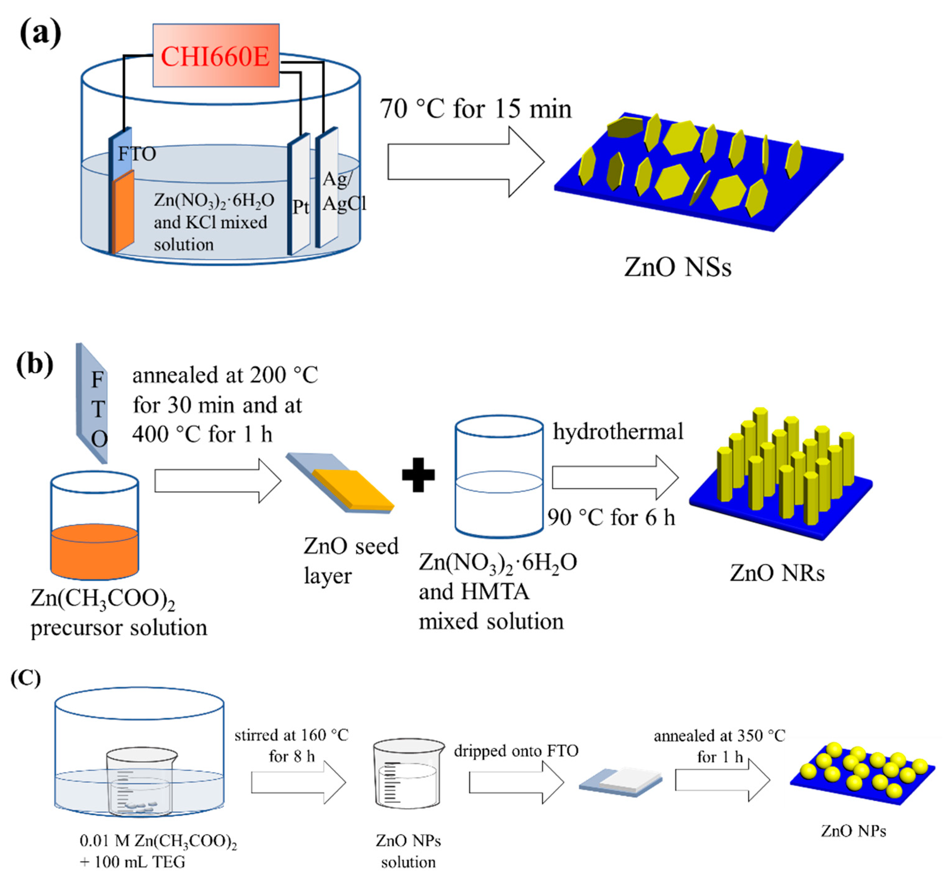
2.1. Preparation of ZnO Nanosheets (ZnO NSs)

The ZnO NSs were synthesized by the electrochemical deposition method in a three-electrode system. Specifically, the working electrode was the fluorine-doped tin oxide (FTO) glass substrate, which was cleaned with acetone, isopropanol, and anhydrous ethanol under sonication for 30 min, respectively, and dried in advance. The counter and reference electrodes were the platinum and Ag/AgCl electrodes, respectively. The solution of electrodeposition was a mixed solution containing zinc nitrate hexahydrate (Zn(NO3)2·6H2O) and potassium chloride (KCl). The concentrations of Zn(NO3)2·6H2O and KCl in the hybrid solution were both 0.1 M. The electrodeposition system was deposited at a deposition potential of −1.1 V for 15 min at 70 °C. Finally, the obtained ZnO NSs samples were cleaned with deionized water and dried at 50 °C for 5 h.

2.2. Preparation of ZnO Nanorods (ZnO NRs)

Preparing the ZnO NRs consisted of two steps. Firstly, preparing the ZnO NRs seed layer. In this step, 3.285 g zinc acetate (Zn(CH3COO)2) was added to 50 mL 2-methoxyethanol (C3H8O2). The solution was stirred at 50 °C. When Zn(CH3COO)2 was completely dissolved in the solution, 1.43 mL ethanolamine (C2H7NO) was added to the solution until the solution was clear. Then, the solution was left to sit for one day. The FTO glass substrates were immersed in the precursor solution for 20 s and then pulled out. The above dip-coating process was repeated 7 times. The substrates were eventually annealed at 200 °C for 30 min and then at 400 °C for 1 h in an air atmosphere. Secondly, the ZnO NRs were grown on the seed layer. The concentration of zinc nitrate hexahydrate (Zn(NO3)2·6H2O) and hexamethylenetetramine (HMTA) in the mixed solution were both 0.05 M. Specifically, the side with the ZnO NRs seed layer was put face down into the hydrothermal reactor. The hybrid solution was added to the hydrothermal reactor with a pipette until the upper edge of the seed layer was covered, and then tightened the hydrothermal reactor. The ZnO NRs samples were obtained by maintaining the growth system at 90 °C for 6 h. Finally, the obtained ZnO NRs samples were cleaned with deionized water and then dried at 80 °C for 1 h.

2.3. Preparation of ZnO Nanospheres (ZnO NPs)

The ZnO NPs were synthesized by the sol-gel method [36,37]. Briefly, 0.01 M Zn(CH3COO)2 was added to 100 mL triethylene glycol (C6H14O4), and then the solution was stirred at 160 °C for 8 h to obtain a colloidal dispersion. Finally, the obtained colloid dispersion was drop-cast onto clean FTO glass and annealed at 350 °C for 1 h.

2.4. Characterization

The morphologies of all the samples at different magnifications were observed using a scanning electron microscope (SEM, SU8010) at an accelerating voltage of 3 kV. The submicroscopic structure and lattice spacing of the samples were observed by transmission electron microscopy and high-resolution transmission electron microscopy (TEM and HRTEM, Tecnai G2 F20) at an accelerating voltage of 200 kV. The phase purity and crystalline structure of the obtained samples were identified by X-ray diffraction (XRD, Empyrean, Cu Kα radiation as the excitation source). The elemental composition and valence states of the samples were characterized by X-ray photoelectron spectroscopy (XPS, ESCALAB 250Xi, Al Kα radiation as the excitation source hν = 1486.6 eV, 150 W, the diameter beam spot is 500 μm). The optical absorbance of the obtained samples was characterized by UV-visible diffuse reflectance spectroscopy (SHIMADZU UV-2600). The efficiency of photoelectron-hole recombination was characterized by the photoluminescence spectra (PL, FLS-1000). The response of materials to light was measured by surface photovoltage spectroscopy (SPV, PL-SPS1000). The PEC performance was measured using a three-electrode system with an electrochemical workstation (CHI660E) and the illumination that was emitted by a solar simulator (300 W xenon lamps, 100 mW/cm2). The working electrode was the obtained samples, the counter electrode was the platinum electrode, and the reference electrode was the Ag/AgCl electrode. The electrolyte was 0.1 M Na2SO4 aqueous solution. The potential of Ag/AgCl was interconverted with the potential of the reversible hydrogen electrode (RHE) by a conversion formula (ERHE = EAg/AgCl + 0.059pH + 0.1976 V, where pH is the pH value of the electrolyte) [38]. The interfacial charge transfer properties of the samples in the solution were characterized by electrochemical impedance spectroscopy (EIS) under illumination. Mott–Schottky (M-S) plots were carried out at a frequency of 1 kHz under illumination. The model piezoelectric potentials under mechanical pressure that were provided by ultrasonic vibrations were simulated by the finite element method (FEM) using COMSOL Multiphysics software.

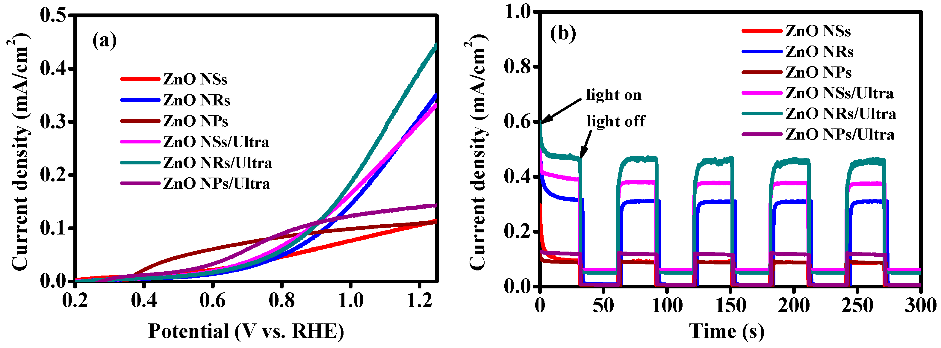
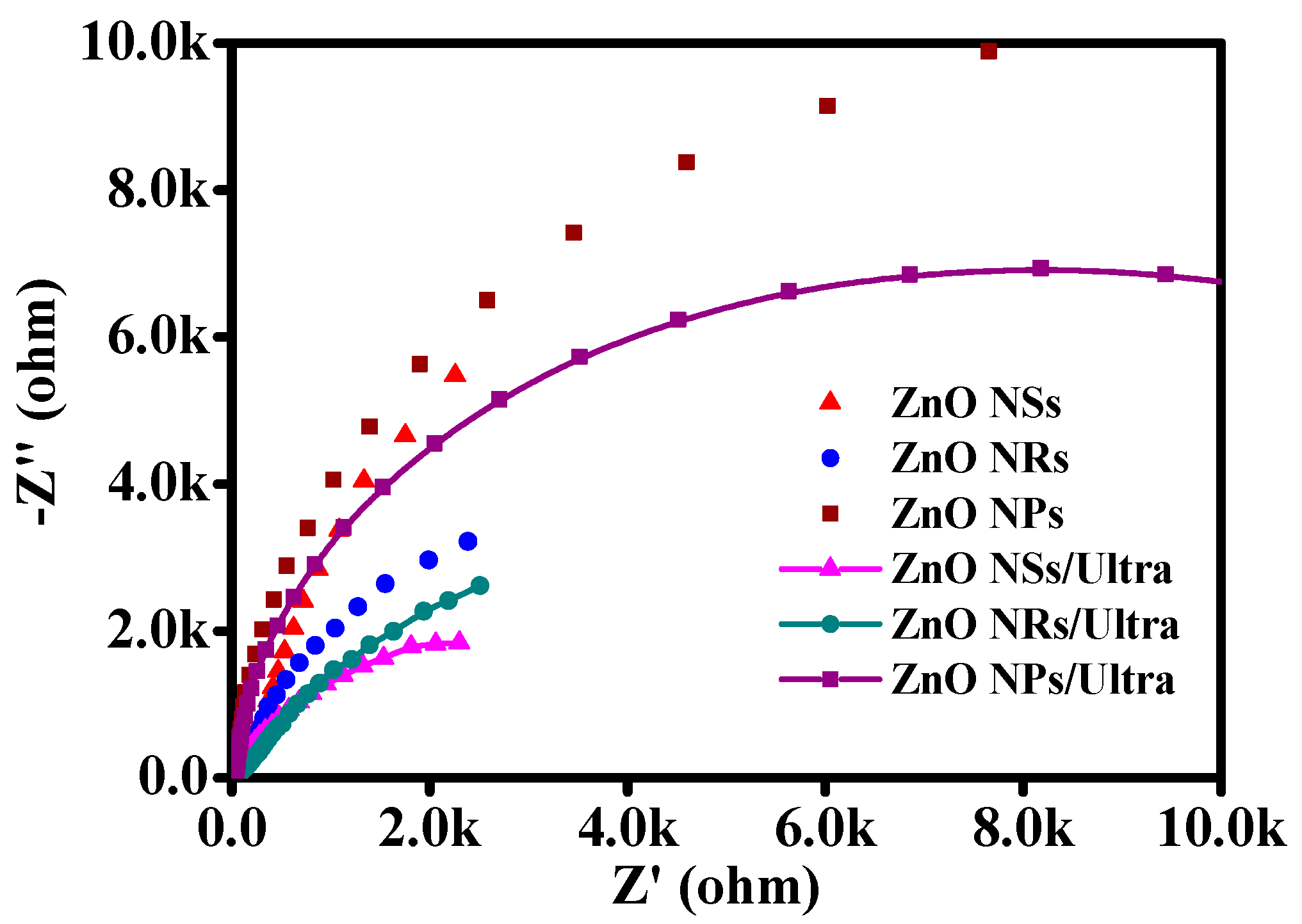
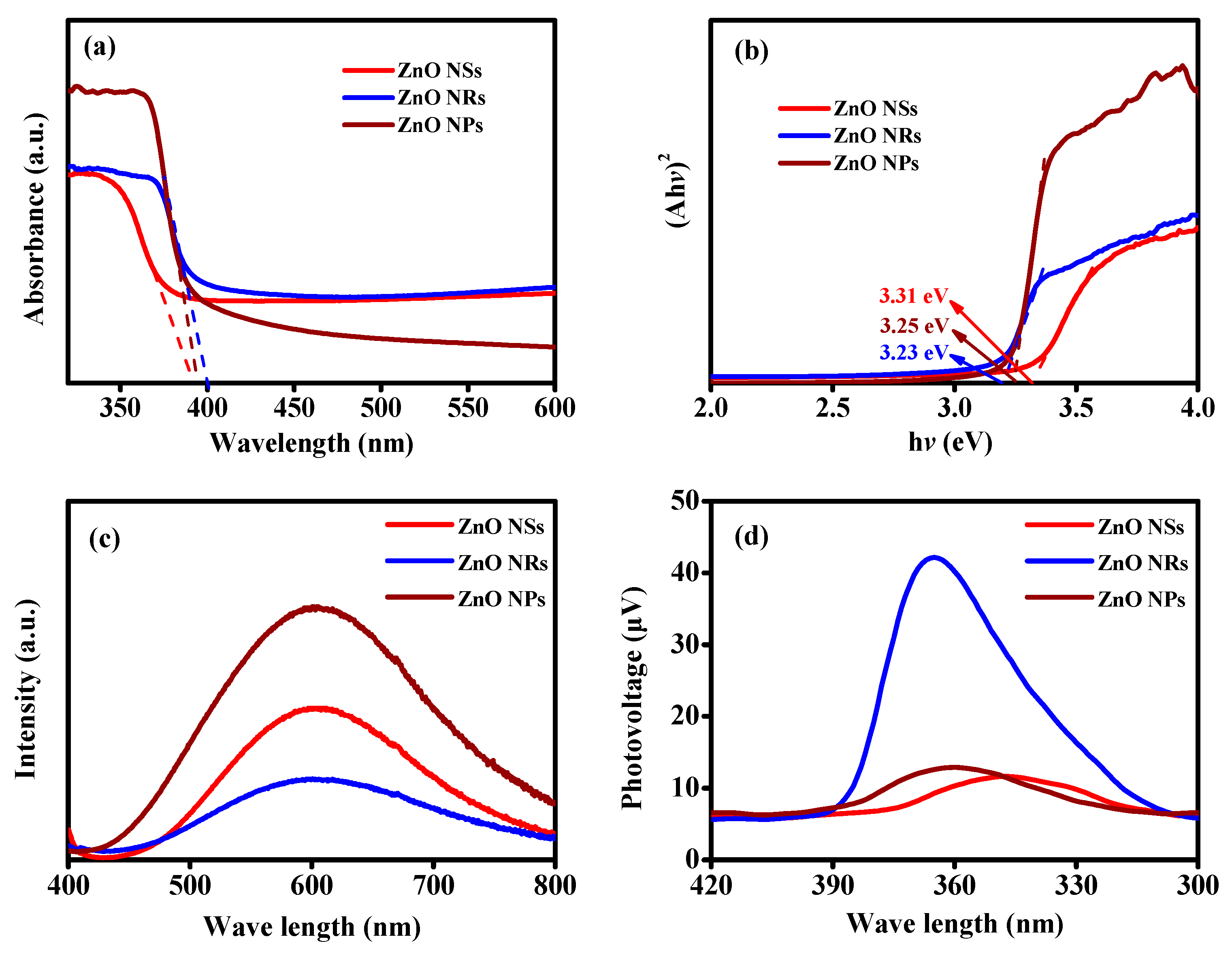
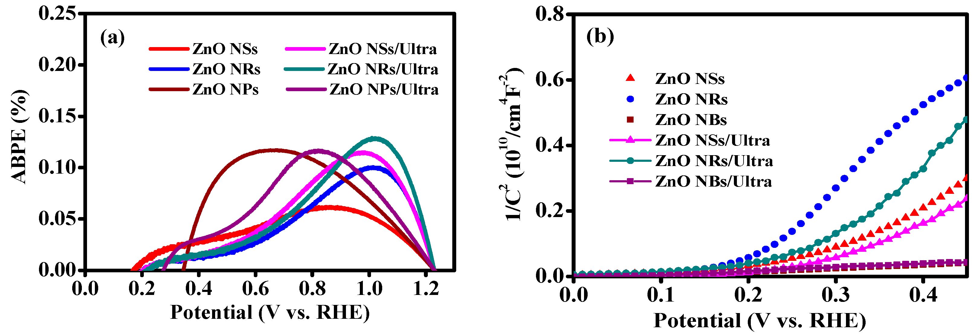
3. Results and Discussion

The fabrication processes of three ZnO photoanodes are illustrated in Figure 1. As shown in Figure 1a, The ZnO NSs were fabricated by electrodeposition using a standard three-electrode setup, and the reaction equations are as follows [39,40]:
Zn(NO3)2 → Zn2+ + 2NO3
NO3 + H2O + 2e → NO2 + 2OH
Zn2+ + 2OH → Zn(OH)2
Zn(OH)2 → ZnO + H2O
In general, the (0001) plane of ZnO (Zn2+-terminated) and −(0001) plane of ZnO (O2--terminated) in the reaction system are high-energy polar surfaces. When ZnO is grown on the FTO glass substrates, the precursor molecules are preferentially adsorbed on the polar surface with minimized surface energy; and then converted to another polar surface with opposite polarity (Zn2+-terminated turned to O2−-terminated and vice versa), resulting in rapid growth along with the [0001] direction [41]. However, KCl in the ZnO NSs growth solution does not directly participate in the ZnO growth reaction; the presence of its Cl ions could be preferentially adsorbed by the (0001) plane of ZnO, which ultimately hinders the conversion of the two polar surfaces and limits the growth of ZnO along the c-axis, resulting in the generation of nanosheet structures [42].
The ZnO NRs were fabricated by the hydrothermal methods (Figure 1b). Green et al. demonstrated that the seed layer of ZnO that was obtained by the thermal decomposition of Zn(CH3COO)2 precursor could get ZnO nanorods arrays vertically [43]. Therefore, the ZnO seed layer was obtained by the thermal decomposition of the Zn(CH3COO)2 precursor solution. Then, the ZnO NRs were prepared by thermal decomposition of Zn(NO3)2·6H2O and HMTA mixed solution, and the reaction equations are as follows [39]:
C6H12N4 (HMTA) + 6H2O → 4NH3 + 6HCHO
NH3 + H2O → NH4+ + OH
Zn2+ + 4NH3 → [Zn(NH3)4]2+
Zn2+ + 2OH → Zn(OH)2
Zn(OH)2 → ZnO + H2O
In the ZnO NRs growth solution, there are no other ions similar to the Cl- ions that are adsorbed by the polar side and HMTA is attached to the non-polar side, promoting the growth of ZnO NRs along the [0001] direction [44]. Furthermore, the HMTA provides a slightly alkaline environment for the growth of ZnO NRs according to reaction Equations (5) and (6).
The ZnO NPs were fabricated by pyrolyzing Zn(CH3COO)2 (Figure 1c). Prolonged stirring is intended to provide a more homogenous dispersion of Zn(CH3COO)2 in the organic solvent, and C6H14O4 has the function of encasing the Zn(CH3COO)2 and preventing its expansion outwards. An improvement in the bonding between the crystals, the film, and the FTO is achieved through high-temperature annealing, which also eliminates organic compounds and converts Zn(CH3COO)2 into ZnO.
Figure 2 presents the morphology of three ZnO nanostructures with typical top-down and cross-sectional views. Figure 2a shows the morphology of ZnO NSs. As presented, ZnO NSs are grown on different lattice planes, and the average hexagonal side length and thickness of each nanosheet are 1320 nm and 60 nm, respectively. Figure 2e is the cross-sectional SEM image of ZnO NSs, from which we can conclude that the film thickness of the ZnO NSs is 1440 nm. On the contrary, most ZnO NRs are grown on one lattice plane, and the average hexagonal side length of each nanosheet is 86 nm, presented in Figure 2b,c. The thickness of the ZnO NRs is 1410 nm, which is concluded from Figure 2f. In addition, from Figure 2d,g, the radius of ZnO NPs is about 150 nm, and the thickness of ZnO NPs is about 1380 nm. Therefore, the film thicknesses of the three ZnO nanostructures are similar.
Moreover, the crystalline structures of the three samples were confirmed by XRD analysis. Figure 3a shows the XRD spectrums of the various ZnO nanostructures that were grown on the FTO substrate, and Figure 3b presents vertically enlarged XRD patterns of the inside of the pink dashed line in Figure 3a. The ZnO NRs peaks are detected at 34.43°, 36.25°, 47.52°, and 62.86°, and they represent lattice planes (002), (101), (102), and (103), respectively. The ZnO NSs peaks are detected at 31.70°, 34.42°, 36.25° and 56.46°, and they represent lattice plane (100), (002), (101) and (110), respectively. Similarly, The ZnO NPs peaks are detected at 31.70°, 34.42°, 36.25°, and 56.46°, and they represent lattice plane (100), (002), (101), and (110), respectively. The detected peaks of three ZnO nanostructures match the standard ZnO diffraction pattern (JCPDS, No. 36-1451), indicating that three morphologies of ZnO have the same crystalline structure, which is a wurtzite structure. Notably, the peak at 34.43° is the highest in the ZnO NRs, indicating that the ZnO NRs are mainly grown on a lattice plane (002). The results of the XRD of three ZnO nanostructures match well with the results of their SEM images.
TEM and HRTEM were measured to investigate further the crystal structure of the three distinct ZnO nanostructures. Figure 4 shows the TEM and HRTEM images of ZnO NRs, ZnO NSs, and ZnO NPs. Figure 4a,b, and c present the low-resolution TEM images of ZnO NRs, ZnO NSs, and ZnO NPs, respectively. It can be seen from the figures that the prepared samples are regular nanorods, nanosheets, and nanospheres. Figure 4d–f present the HRTEM images of three nanostructures. In Figure 4d, the lattice distance of 2.82 nm, 2.60 nm, and 2.48 nm corresponds to the (100), (002), and (101) planes of the ZnO NSs, severally. Similarly, the lattice distance of 2.60 nm and 2.48 nm in Figure 4e corresponds to the (002) and (101) planes of the ZnO NRs, respectively. In Figure 4f, the lattice distance of 2.81 nm, 2.62nm, 2.47 nm, and 1.93 nm corresponds to the (100), (002), (101), and (102) planes of the ZnO NSs, respectively. These results match the findings from XRD well.
As displayed in Figure 5, XPS was used to investigate the chemical states of three samples. Firstly, the XPS survey scan spectrum of three samples exhibited distinct Zn 2p, O 1s, and C 1s core-level peaks in Figure 5a. Then, the valence states analysis of each element is displayed in Figure 5b–d. All the elements are recalibrated according to C 1s located at 284.8 eV (Figure 5b). According to Figure 5c, the binding energies of three samples for Zn 2p3/2 and Zn 2p1/2 are the same, located at 1021.4 eV and 1044.6 eV, respectively, indicating that zinc is in the Zn2+ state. As shown in Figure 5d, the binding energies of three ZnO samples for O1s consisted of two different binding energy components. The low binding energy component is typically attributed to lattice oxygen, and the high binding energy one to –OH surface groups due to the exposure of the sample to the atmosphere and water vapor from the synthesis process [45,46,47]. Therefore, it proves that the three samples are ZnO and have no other impurity components.
Furthermore, the absorption of light by the samples was measured by UV-vis spectra, and the results are shown in Figure 6a. The light absorption ranges of the ZnO NSs, ZnO NRs, and ZnO NPs are 380 nm, 390 nm, and 385 nm, respectively. Moreover, the optical bandgaps of the samples were calculated according to the following formula [48,49]:
(Ahv)n = K (hv − Eg)
where A is the absorption coefficient, h is Planck’s constant, v is the frequency of the light, K is a constant, Eg (eV) is the band gap energy of the semiconductor, and n is related to the type of semiconductors, n = 2 for a direct-gap semiconductor and n = 1/2 for an indirect-gap semiconductor. Since ZnO is a direct-gap semiconductor, the value of n is 2. Figure 6b shows the plot of (Ahv)2-hv of three ZnO samples. The bandgaps of the ZnO NSs, ZnO NRs, and ZnO NPs are calculated to be 3.31 eV, 3.23 eV, and 3.25 eV, respectively. The different results could be attributed to the Burstein–Moss shift [50,51], and the results are close to the bandgap of ZnO in previous studies [24,52]. The photoelectron-hole recombination efficiency was investigated using PL, and the findings are presented in Figure 6c. Among the three samples, the ZnO NRs possess the lowest peak intensity; it represents the least efficient photoelectron-hole recombination within ZnO NRs, due to a strong peak intensity which indicates a high photoelectron-hole recombination efficiency [53]. Figure 6d shows the results of three samples that were characterized by SPV. The response range of nanosheets to light is significantly narrower than that of nanorods and nanospheres, which is consistent with the UV-Vis absorption spectra data (in Figure 6a). Besides, the photovoltage of the ZnO NRs is the highest, and that of the ZnO NSs and NPs are similar. Therefore, the ZnO NRs exhibit the greatest photoelectrochemical performance among the three samples because of their broad optical absorption and low photoelectron-hole recombination efficiency.
The photoelectrochemical properties of the three samples changed differently after adding the piezoelectric effect. We measured the photocurrent density-voltage curves (Figure 7a) and I-T curves under intermittent illumination with the applied bias at 1.23 V vs. RHE (Figure 7b). There were three obtained samples that were immersed in 0.1 M Na2SO4 electrolyte as working electrodes, and the area of them was 1 cm2. The photocurrent of the as-prepared ZnO NSs, ZnO NRs, and ZnO NPs were 0.11 mA/cm2, 0.30 mA/cm2, and 0.10 mA/cm2 at 1.23 V vs. RHE, respectively. After the addition of ultrasonic vibrations, the photocurrent of the ZnO NSs, ZnO NRs, and ZnO NPs increased to 0.32 mA/cm2, 0.41 mA/cm2, and 0.12 mA/cm2 at 1.23 V vs. RHE, respectively. Consequently, the piezo-photoelectrochemical performance of ZnO NSs was enhanced by a factor of 3 times, nanorods were a factor of 1.4 times, and nanospheres were a factor of 1.2 times. The piezo-photoelectrochemical performance of three samples is more clearly displayed in Figure 7b. When the light was turned off, there was no current in any of the three samples, and when ultrasonic vibrations were applied, all three samples exhibited an increase in current. The increasing current density is largely explained by the ZnO crystals lacking inversion symmetry, and a non-zero dipole moment is created within the lattice, which results in a strain-induced polarized electric field when ZnO is deformed by force [54]. The polarized electric field that is produced by the ultrasonic vibrations efficiently promotes carrier separation, allowing the samples to generate current even in the dark. Notably, among the three samples, the light absorption range of ZnO NRs is the widest (390 nm, Figure 6a,d), but the improvement of the photoelectrochemical performance is not the highest under the piezoelectric effect. Therefore, these results indicate that the piezoelectric effect could improve the photoelectrochemical water splitting of ZnO, and the morphology of ZnO is the main factor that affects the piezo-photoelectrochemical performance compared to the light absorption range of ZnO.
The interfacial charge transfer properties of the samples in solution were characterized by EIS under illumination, and the results are shown in Figure 8. The curves in Figure 8 are the measured results of the three different nanostructured ZnO samples under illumination and illumination with ultrasonic vibrations, respectively. The radius of the curves for the three samples with ultrasonic vibrations is less than without ultrasonic vibrations, indicating that the charge transfer rates of the three samples with ultrasonic vibrations are faster than those without ultrasonic vibrations. This result is because the diameter of the fitted semicircle in EIS equals the electron transport resistance, and a semicircle with a small radius denotes a low charge transfer resistance [55,56]. Besides, the diameter of the ZnO NSs with ultrasonic vibrations is smaller than that of the other two samples with ultrasonic vibrations, indicating that the charge transfer rate of the ZnO NSs is the fastest in the three samples under ultrasonication. These results suggest that the electron transfer efficiency of ZnO is enhanced under ultrasonication. Meanwhile, ultrasonic vibrations have different effects on the electron transfer efficiency of ZnO with different nanostructures.
The applied bias photon–current efficiency (ABPE) curve based on photocurrent density is used to quantitatively evaluate the efficiency of PEC water splitting of three samples, which is calculated by the following formula [57]:
η (%) = [J × (1.23 − Vapp)/Plight] × 100%
where J incidents the obtained photocurrent density under illumination, Vapp represents the applied electric bias, and Plight means light intensity. As shown in Figure 9a, the photoelectric conversion efficiency of the ZnO NSs under ultrasonic vibrations reached 0.12%, which is 1.62 times higher than that of the ZnO NSs without ultrasonic vibrations (0.07%), that of the ZnO NRs only improved by 1.13 times under ultrasonic vibrations (from 0.13% to 0.15%). Instead, the photoelectric conversion efficiency of the ZnO NPs remained unchanged. In addition, Figure 9b represents the Mott–Schottky (M-S) curves under illumination to determine the charge density. The curves of all the samples display positive slopes, which means that all the samples are n-type semiconductors. The carrier density (Nd) can be calculated using the slope value with the following formula [58]:
Nd = (2/eεε0)/[d((1/C2)/dV]
where e, ε, and ε0 represent the charge of the electronic, the dielectric constant of ZnO, and the vacuum permittivity, respectively. It can be seen that a small slope value represents a high carrier concentration from Formula (12). As shown in Figure 9b, the samples of the ZnO NSs and NRs have smaller slope values under ultrasonic vibrations, which indicates that ultrasonic vibrations are beneficial to increase the concentration of electrons. That is because the deformation of the ZnO NSs and ZnO NRs caused by ultrasonic vibrations generates a built-in electric field in the ZnO photoanode, which accelerates the separation of electrons and reduces the recombination of electrons and holes. However, the two M-S curves of the ZnO NPs almost overlap, which indicates that the carrier concentration of the ZnO NPs is also not greatly improved under ultrasonic vibrations.
From the above, the thickness of the three sample films is similar, the composition of the three samples is the same, the area that is immersed in the electrolyte during detection is the same, and the differences are their morphologies and the light absorption ranges. However, according to results in Figure 6d and Figure 7b, the morphology of ZnO has a greater influence than the light absorption range. Therefore, we conclude that the ZnO NSs have a better effect in piezo-photoelectrochemical water splitting, which is related to the morphology of ZnO.
Moreover, for better visualization of the piezoelectric potential that is produced by the three samples under ultrasound, the FEM simulation was performed on all the samples. The parameters of the model were set based on the morphologies of three samples in Figure 2. The hexagon side length and thickness were set to 86 nm × 1410 nm and 1320 nm × 60 nm for the ZnO NRs and NSs, respectively. The radius of the ZnO NPs was set to 150 nm. A local high pressure (100 MPa) was due to the collapse of bubbles that were generated in the water under ultrasonic vibrations [59,60]. Thus, the FEM simulation was carried out at a pressure of 100 MPa. The direction in which the pressure is applied is determined by the exposed crystallographic orientation. Therefore, the bottom of the model was fixed and grounded, and a pressure of 100 MPa was applied to the surface of the model along the negative z-axis and perpendicular to the z-axis; the simulation results are shown in Figure 10a–c. The maximum potential of the ZnO NSs is 0.6 V (Figure 10a), which is higher than that of the ZnO NRs (0.2 V, Figure 10b) and ZnO NPs (0.04 V, Figure 10c). The results show that compared to the ZnO NRs and ZnO NPs, the ZnO NSs were deformed easily and generated high potential under ultrasonic vibrations, which can effectively accelerate the separation of photogenerated carriers. The results of the FEM simulation are consistent with the above experimental results, which explain the phenomenon successfully that the photoelectrochemical performance efficiency of the ZnO NSs is improved more than that of the ZnO NRs and ZnO NPs under ultrasonic vibrations.
To visually explain the reason the morphology of ZnO affects piezo-photoelectrochemical performance, Figure 10d shows a schematic diagram of ZnO deformation under ultrasonic vibrations. The direction of stress that is generated by ultrasonic vibrations is divided into vertical forces (Fv) that are perpendicular to the FTO direction and horizontal forces (Fh) parallel to the FTO direction. Since the ZnO NRs are regular hexagonal prisms with relatively uniform sides, the forces Fh in the horizontal direction mostly cancel each other out, and the forces Fv in the vertical direction play a significant part in the deformation of the ZnO NRs when ultrasonic vibrations occur on the ZnO NRs. In contrast, since ZnO NSs are sheet-like structures, they do not grow perpendicular to the FTO and are unevenly distributed on each side. The forces Fh do not cancel each other in the horizontal direction, resulting in a pressure difference that deforms the ZnO NSs in the horizontal direction. The forces Fv still deform the NSs in the vertical direction. Therefore, ZnO NSs will be deformed due to the forces acting in two directions. However, due to the spherical structure of ZnO NPs, the surface of ZnO NPs is more uniform than that of ZnO NRs and NSs. Most of the forces (Fh and Fv) in the horizontal and vertical directions will cancel each other out so that the effective stress of the deformation of ZnO NPs is very slight.
In short, the ZnO NSs are deformed by force in two directions (Fh and Fv), while the ZnO NRs are in only one direction (Fv), and the ZnO NPs are deformed by little force. This results in the ZnO NSs being more easily bent with a larger amount of deformation so that the ZnO NSs have more excellent surface piezoelectric potential to make them better to accelerate the separation of charges and improve PEC performance.

4. Conclusions

In summary, three different nanostructures of ZnO were used as piezoelectric material models to investigate the influence of the morphology of ZnO on enhancing photoelectrochemical water splitting performance under the piezoelectric effect. Compared to the ZnO NRs and ZnO NPs, the ZnO NSs are subjected to higher effective deformation stress under ultrasonic vibrations due to their non-axial vertical growth, making them more susceptible to deformation and a larger piezoelectric potential, which accelerates the charge separation efficiency of the ZnO NSs and improves photocatalytic performance by a factor of three times. In addition, finite element simulation was used to confirm the effect of the morphology of ZnO on the piezoelectric effect to enhance the photocatalytic performance. This study provides a new idea and reference for the subsequent design of different photoelectrodes in piezo-photoelectrochemical water splitting.

Author Contributions

Conceptualization, D.W. and Z.L.; methodology, D.W.; software, D.W.; validation, D.W., R.L. and Q.F.; formal analysis, C.H.; investigation, D.W.; resources, B.T.; data curation, D.W.; writing—original draft preparation, D.W.; writing—review and editing, Z.L.; visualization, D.W.; supervision, C.H.; project administration, Z.L.; funding acquisition, C.H. All authors have read and agreed to the published version of the manuscript.

Funding

This research was funded by the Open Foundation of Hubei Collaborative Innovation Center for High-efficient Utilization of Solar Energy (grant no. HBSKFZD2017001) and the National Science Foundation of China (grant no. 52103339).

Data Availability Statement

Not applicable.

Conflicts of Interest

The authors declare no conflict of interest.

References

  1. Cai, Q.J.; Liu, Z.F.; Han, C.C.; Tong, Z.F.; Ma, C.H. CuInS2/Sb2S3 heterostructure modified with noble metal co-catalyst for efficient photoelectrochemical water splitting. J. Alloy. Compd. 2019, 795, 319–326. [Google Scholar] [CrossRef]
  2. Fang, G.Z.; Liu, Z.F.; Han, C.C. Enhancing the PEC water splitting performance of BiVO4 co-modifying with NiFeOOH and Co-Pi double layer cocatalysts. Appl. Surf. Sci. 2020, 515, 146095. [Google Scholar] [CrossRef]
  3. Shi, L.; Yin, Y.; Zhang, L.C.; Wang, S.B.; Sillanpaa, M.; Sun, H.Q. Design and engineering heterojunctions for the photoelectrochemical monitoring of environmental pollutants: A review. Appl. Catal. B-Environ. 2019, 248, 405–422. [Google Scholar] [CrossRef]
  4. Zhang, S.C.; Liu, Z.F.; Ruan, M.N.; Guo, Z.G.; Lei, E.; Zhao, W.; Zhao, D.; Wu, X.F.; Chen, D.M. Enhanced piezoelectric-effect-assisted photoelectrochemical performance in ZnO modified with dual cocatalysts. Appl. Catal. B-Environ. 2020, 262, 118279. [Google Scholar] [CrossRef]
  5. Fujishima, A.; Honda, K. Electrochemical photolysis of water at a semiconductor Electrode. Nature 1972, 238, 37–38. [Google Scholar] [CrossRef] [PubMed]
  6. Shabdan, Y.; Markhabayeva, A.; Bakranov, N.; Nuraje, N. Photoactive tungsten-oxide nanomaterials for water-splitting. Nanomaterials 2020, 10, 1871. [Google Scholar] [CrossRef] [PubMed]
  7. Liu, C.; Su, J.Z.; Zhou, J.L.; Guo, L.J. A multistep ion exchange approach for fabrication of porous BiVO4 nanorod arrays on transparent conductive substrate. ACS Sustain. Chem. Eng. 2016, 4, 4492–4497. [Google Scholar] [CrossRef]
  8. Wang, G.M.; Wang, H.Y.; Ling, Y.C.; Tang, Y.C.; Yang, X.Y.; Fitzmorris, R.C.; Wang, C.C.; Zhang, J.Z.; Li, Y. Hydrogen-treated TiO2 nanowire arrays for photoelectrochemical water splitting. Nano Lett. 2011, 11, 3026–3033. [Google Scholar] [CrossRef]
  9. Chen, D.; Liu, Z.F.; Zhou, M.; Wu, P.D.; Wei, J.D. Enhanced photoelectrochemical water splitting performance of alpha-Fe2O3 nanostructures modified with Sb2S3 and cobalt phosphate. J. Alloy. Compd. 2018, 74, 2918–2927. [Google Scholar]
  10. Wang, P.; Liu, Z.F.; Chen, D.; Zhang, S.C.; Fang, G.Z.; Han, C.C.; Cheng, Z.W.; Tong, Z.F. An unassisted tandem photoelectrochemical cell based on p- and n-Cu2O Photoelectrodes. Catal. Lett. 2021, 151, 1976–1983. [Google Scholar] [CrossRef]
  11. Toghraie, D.; Mahmoudi, M.; Akbari, O.A.; Pourfattah, F.; Heydari, M. The effect of using water/CuO nanofluid and L-shaped porous ribs on the performance evaluation criterion of microchannels. J. Therm. Anal. Calorim. 2019, 135, 145–159. [Google Scholar] [CrossRef]
  12. Ma, H.P.; Zhang, J.; Liu, Z.F. Efficient tungsten oxide/bismuth oxyiodide core/shell photoanode for photoelectrochemical water splitting. Appl. Surf. Sci. 2017, 423, 63–70. [Google Scholar] [CrossRef]
  13. Berglund, S.P.; Abdi, F.F.; Bogdanoff, P.; Chernseddine, A.; Friedrich, D.; van de Krol, R. Comprehensive evaluation of CuBi2O4 as a photocathode material for photoelectrochemical water splitting. Chem. Mater. 2016, 28, 4231–4242. [Google Scholar] [CrossRef]
  14. Jiang, C.R.; Moniz SJ, A.; Wang, A.Q.; Zhang, T.; Tang, J.W. Photoelectrochemical devices for solar water splitting—Materials and challenges. Chem. Soc. Rev. 2017, 46, 4645–4660. [Google Scholar] [CrossRef] [PubMed] [Green Version]
  15. Osterloh, F.E. Inorganic nanostructures for photoelectrochemical and photocatalytic water splitting. Chem. Soc. Rev. 2013, 42, 2294–2320. [Google Scholar] [CrossRef]
  16. Yang, Y.; Niu, S.W.; Han, D.D.; Liu, T.Y.; Wang, G.M.; Li, Y. Progress in developing metal oxide nanomaterials for photoelectrochemical water splitting. Adv. Energy Mater. 2017, 7, 1700555. [Google Scholar] [CrossRef]
  17. Li, C.L.; Cao, Q.; Wang, F.Z.; Xiao, Y.Q.; Li, Y.B.; Delaunay, J.J.; Zhu, H.W. Engineering graphene and TMDs based van der Waals heterostructures for photovoltaic and photoelectrochemical solar energy conversion. Chem. Soc. Rev. 2018, 47, 4981–5037. [Google Scholar] [CrossRef]
  18. Zhang, X.; Liu, Y.; Lee, S.T.; Yang, S.H.; Kang, Z.H. Coupling surface plasmon resonance of gold nanoparticles with slow-photon-effect of TiO2 photonic crystals for synergistically enhanced photoelectrochemical water splitting. Energy Environ. Sci. 2014, 7, 1409–1419. [Google Scholar] [CrossRef]
  19. Shen, S.H.; Jiang, J.G.; Guo, P.H.; Kronawitter, C.X.; Mao, S.S.; Guo, L.J. Effect of Cr doping on the photoelectrochemical performance of hematite nanorod photoanodes. Nano Energy 2012, 1, 732–741. [Google Scholar] [CrossRef]
  20. Zhang, S.S.; Yan, J.; Yang, S.Y.; Xu, Y.H.; Cai, X.; Li, X.; Zhang, X.C.; Peng, F.; Fang, Y.P. Electrodeposition of Cu2O/g-C3N4 heterojunction film on an FTO substrate for enhancing visible light photoelectrochemical water splitting. Chin. J. Catal. 2017, 38, 365–371. [Google Scholar] [CrossRef]
  21. Li, Y.T.; Liu, Z.F.; Guo, Z.G.; Ruan, M.N.; Li, X.F.; Liu, Y.L. Efficient WO3 photoanode modified by Pt layer and plasmonic Ag for enhanced charge separation and transfer to promote photoelectrochemical performances. ACS Sustain. Chem. Eng. 2019, 7, 12582–12590. [Google Scholar] [CrossRef]
  22. Liu, Z.R.; Yu, X.; Li, L.L. Piezopotential augmented photo- and photoelectro-catalysis with a built-in electric field. Chin. J. Catal. 2020, 41, 534–549. [Google Scholar] [CrossRef]
  23. Yan, X.H.; Li, G.; Wang, Z.Y.; Yu, Z.C.; Wang, K.Y.; Wu, Y.C. Recent progress on piezoelectric materials for renewable energy conversion. Nano Energy 2020, 77, 105180. [Google Scholar] [CrossRef]
  24. Pan, L.; Sun, S.C.; Chen, Y.; Wang, P.H.; Wang, J.Y.; Zhang, X.W.; Zou, J.J.; Wang, Z.L. Advances in piezo-phototronic effect enhanced photocatalysis and photoelectrocatalysis. Adv. Energy Mater. 2020, 10, 2000214. [Google Scholar] [CrossRef]
  25. You, J.K.; Liu, Z.F.; Guo, Z.G.; Ruan, M.N.; Yan, W.G. Doping of W ions to modulate the polarization intensity of Bi2WO6 for efficient piezoelectric-photoelechochemical water splitting. ACS Appl. Energy Mater. 2022, 5, 11472–11482. [Google Scholar] [CrossRef]
  26. Shi, J.; Starr, M.B.; Xiang, H.; Hara, Y.; Anderson, M.A.; Seo, J.H.; Ma, Z.Q.; Wang, X.D. Interface engineering by piezoelectric potential in ZnO-based photoelectrochemical anode. Nano Lett. 2011, 11, 5587–5593. [Google Scholar] [CrossRef]
  27. Kumar, D.; Sharma, S.; Khare, N. Piezo-phototronic and plasmonic effect coupled Ag-NaNbO3 nanocomposite for enhanced photocatalytic and photoelectrochemical water splitting activity. Renew. Energy 2021, 163, 1569–1579. [Google Scholar] [CrossRef]
  28. Zhao, Q.Y.; Liu, Z.F.; Guo, Z.G.; Ruan, M.N.; Yan, W.G. The collaborative mechanism of surface S-vacancies and piezoelectric polarization for boosting CdS photoelectrochemical performance. Chem. Eng. J. 2022, 433, 133226. [Google Scholar] [CrossRef]
  29. Zhao, W.; Zhang, Q.; Wang, H.G.; Rong, J.C.; Lei, E.; Dai, Y.J. Enhanced catalytic performance of Ag2O/BaTiO3 heterostructure microspheres by the piezo/pyro-phototronic synergistic effect. Nano Energy 2020, 73, 104783. [Google Scholar] [CrossRef]
  30. Goel, S.; Kumar, B. A review on piezo-/ferro-electric properties of morphologically diverse ZnO nanostructures. J. Alloy. Compd. 2020, 816, 152491. [Google Scholar] [CrossRef]
  31. Koutavarapu, R.; Babu, B.; Reddy, C.V.; Reddy, I.N.; Reddy, K.R.; Rao, M.C.; Aminabhavi, T.M.; Cho, M.; Kim, D.; Shim, J. ZnO nanosheets-decorated Bi2WO6 nanolayers as efficient photocatalysts for the removal of toxic environmental pollutants and photoelectrochemical solar water oxidation. J. Environ. Manag. 2020, 265, 110504. [Google Scholar] [CrossRef] [PubMed]
  32. Gill, R.; Ghosh, S.; Sharma, A.; Kumar, D.; Nguyen, V.H.; Vo DV, N.; Pham, T.D.; Kumar, P. Vertically aligned ZnO nanorods for photoelectrochemical water splitting application. Mater. Lett. 2020, 277, 128295. [Google Scholar] [CrossRef]
  33. Li, J.L.; Jin, B.J.; Jiao, Z.B. Rationally embedded zinc oxide nanospheres serving as electron transport channels in bismuth vanadate/zinc oxide heterostructures for improved photoelectrochemical efficiency. J. Colloid Interface Sci. 2021, 592, 127–134. [Google Scholar] [CrossRef]
  34. Hong, K.S.; Xu, H.F.; Konishi, H.; Li, X.C. Direct water splitting through vibrating piezoelectric microfibers in water. J. Phys. Chem. Lett. 2010, 1, 997–1002. [Google Scholar] [CrossRef]
  35. Chen, Y.; Wang, L.; Gao, R.J.; Zhang, Y.C.; Pan, L.; Huang, C.Y.; Liu, K.; Chang, X.Y.; Zhang, X.W.; Zou, J.J. Polarization-enhanced direct Z-scheme ZnO-WO3-x nanorod arrays for efficient piezoelectric-photoelectrochemical water splitting. Appl. Catal. B-Environ. 2019, 259, 118079. [Google Scholar] [CrossRef]
  36. Jézéquel, D.; Guenot, J.; Jouini, N.; Fiévet, F. Submicrometer zinc oxide particles: Elaboration in polyol medium and morphological characteristics. J. Mater. Res. 1995, 10, 77–83. [Google Scholar] [CrossRef]
  37. Zhang, Q.F.; Chou, T.P.; Russo, B.; Jenekhe, S.A.; Cao, G.Z. Aggregation of ZnO nanocrystallites for high conversion efficiency in dye-sensitized solar cells. Angew. Chem. Int. Ed. 2008, 47, 2402–2406. [Google Scholar] [CrossRef]
  38. Liu, R.; Wang, D.; Han, C.C.; Wang, P.; Tong, Z.F.; Tan, B.H.; Liu, Z.F. The synergistic effect of CuBi2O4 and Co-Pi: Improving the PEC activity of BiVO4-based composite materials. New J. Chem. 2022, 46, 2971–2979. [Google Scholar] [CrossRef]
  39. Skompska, M.; Zarebska, K. Electrodeposition of ZnO nanorod arrays on transparent conducting substrates-a review. Electrochim. Acta 2014, 127, 467–488. [Google Scholar] [CrossRef]
  40. Messai, Z.; Ouennoughi, Z.; Devers, T.; Mouet, T.; Harel, V.; Konstantinov, K.; Bouguechal, N. Growth and characteristics of ZnO nano-aggregates electrodeposited onto p-Si(111). Appl. Surf. Sci. 2010, 257, 616–621. [Google Scholar] [CrossRef]
  41. Laudise, R.A.; Ballman, A.A. Hydrothermal synthesis of zinc oxide and zinc sulfide. J. Phys. Chem. 1960, 64, 688–691. [Google Scholar] [CrossRef]
  42. Tena-Zaera, R.; Elias, J.; Wang, G.; Lévy-Clément, C. Role of chloride ions on electrochemical deposition of ZnO nanowire arrays from O2 reduction. J. Phys. Chem. C 2007, 111, 16706–16711. [Google Scholar] [CrossRef]
  43. Greene, L.E.; Law, M.; Tan, D.H.; Montano, M.; Goldberger, J.; Somorjai, G.; Yang, P.D. General route to vertical ZnO nanowire arrays using textured ZnO seeds. Nano Lett. 2005, 5, 1231–1236. [Google Scholar] [CrossRef] [PubMed]
  44. Xu, S.; Wang, Z.L. One-dimensional ZnO nanostructures: Solution growth and functional properties. Nano Res. 2011, 4, 1013–1098. [Google Scholar] [CrossRef] [Green Version]
  45. Barreca, D.; Bekermann, D.; Comini, E.; Devi, A.; Fischer, R.A.; Gasparotto, A.; Maccato, C.; Sberveglieri, G.; Tondello, E. 1D ZnO nano-assemblies by Plasma-CVD as chemical sensors for flammable and toxic gases. Sens. Actuators B Chem. 2010, 149, 1–7. [Google Scholar] [CrossRef]
  46. Barreca, D.; Ferrucci, A.P.; Gasparotto, A.; Maccato, C.; Maragno, C.; Tondello, E. Temperature-controlled synthesis and photocatalytic performance of ZnO nanoplatelets. Chem. Vap. Depos. 2007, 13, 618–625. [Google Scholar] [CrossRef]
  47. Bekermann, D.; Gasparotto, A.; Barreca, D.; Devi, A.; Fischer, R.A.; Kete, M.; Lavrenčič, Š.U.; Lebedev, O.I.; Maccato, C.; Van Tendeloo, G. ZnO nanorod arrays by plasma-enhanced CVD for light-activated functional applications. ChemPhysChem 2010, 11, 2337–2340. [Google Scholar] [CrossRef]
  48. Peng, Q.; Wang, J.; Wen, Y.W.; Shan, B.; Chen, R. Surface modification of LaFeO3 by Co-Pi electrochemical deposition as an efficient photoanode under visible light. RSC Adv. 2016, 6, 26192–26198. [Google Scholar] [CrossRef]
  49. Zhang, Z.H.; Hossain, M.F.; Takahashi, T. Self-assembled hematite (alpha-Fe2O3) nanotube arrays for photoelectrocatalytic degradation of azo dye under simulated solar light irradiation. Appl. Catal. B-Environ. 2010, 95, 423–429. [Google Scholar] [CrossRef]
  50. Burstein, E. Anomalous optical absorption limit in InSb. Phys. Rev. 1954, 93, 632. [Google Scholar] [CrossRef]
  51. Lai, F.C.; Lin, L.M.; Gai, R.Q.; Lin, Y.Z.; Huang, Z.G. Determination of optical constants and thicknesses of In2O3:Sn films from transmittance data. Thin Solid Film. 2007, 515, 7387–7392. [Google Scholar] [CrossRef]
  52. Hsu, Y.K.; Chen, Y.C.; Lin, Y.G. Novel ZnO/Fe2O3 Core-Shell Nanowires for Photoelectrochemical Water Splitting. ACS Appl. Mater. Interfaces 2015, 7, 14157–14162. [Google Scholar] [CrossRef] [PubMed]
  53. Zhou, H.M.; Chen, R.L.; Han, C.C.; Wang, P.; Tong, Z.F.; Tan, B.H.; Huang, Y.Z.; Liu, Z.F. Copper phosphide decorated g-C3N4 catalysts for highly efficient photocatalytic H2 evolution. J. Colloid Interface Sci. 2022, 610, 126–135. [Google Scholar] [CrossRef]
  54. Lim, T.; Ico, G.; Jung, K.; Bozhilov, K.N.; Nam, J.; Martinez-Morales, A.A. Crystal growth and piezoelectric characterization of mechanically stable ZnO nanostructure arrays. Crystengcomm 2018, 20, 5688–5694. [Google Scholar] [CrossRef] [Green Version]
  55. Cao, S.Y.; Yan, X.Q.; Kang, Z.; Liang, Q.J.; Liao, X.Q.; Zhang, Y. Band alignment engineering for improved performance and stability of ZnFe2O4 modified CdS/ZnO nanostructured photoanode for PEC water splitting. Nano Energy 2016, 24, 25–31. [Google Scholar] [CrossRef]
  56. Fang, G.Z.; Liu, Z.F.; Han, C.C.; Ma, X.G.; Lv, H.; Huang, C.Y.; Cheng, Z.W.; Tong, Z.F.; Wang, P. The CoNiO2 as a novel water oxidation cocatalyst to enhance PEC water splitting performance of BiVO4. Chem. Commun. 2020, 56, 9158–9161. [Google Scholar] [CrossRef] [PubMed]
  57. Asha, K.; Satsangi, V.R.; Shrivastav, R.; Kant, R.; Dass, S. Effect of morphology and impact of the electrode/electrolyte interface on the PEC response of Fe2O3 based systems—Comparison of two preparation techniques. RSC Adv. 2020, 10, 42256–42266. [Google Scholar] [CrossRef]
  58. Khan, S.U.; Perini, J.A.L.; Hussain, S.; Khan, H.; Khan, S.; Zanoni, M.V.B. Electrochemical preparation of Nb2O5 nanochannel photoelectrodes for enhanced photoelectrocatalytic performance in removal of RR120 dye. Chemosphere 2020, 257, 127164. [Google Scholar] [CrossRef]
  59. Li, H.D.; Sang, Y.H.; Chang, S.J.; Huang, X.; Zhang, Y.; Yang, R.S.; Jiang, H.D.; Liu, H.; Wang, Z.L. Enhanced ferroelectric-nanocrystal-based hybrid photocatalysis by ultrasonic-wave-generated piezophototronic effect. Nano Lett. 2015, 15, 2372–2379. [Google Scholar] [CrossRef]
  60. Wu, J.; Qin, N.; Bao, D.H. Effective enhancement of piezocatalytic activity of BaTiO3 nanowires under ultrasonic vibration. Nano Energy 2018, 45, 44–51. [Google Scholar] [CrossRef]
Figure 1. Schematic illustration for the fabrication process of (a) ZnO NSs, (b) ZnO NRs, and (c) ZnO NPs photoanode.
Inorganics 11 00011 g001
Figure 2. The morphologies of three ZnO nanostructures. SEM image of (a) ZnO NSs, (b,c) ZnO NRs, and (d) ZnO NPs. Cross-sectional SEM image of (e) ZnO NSs, (f) ZnO NRs, and (g) ZnO NPs.
Inorganics 11 00011 g002
Figure 3. (a) XRD patterns of three ZnO samples. (b) Vertically enlarged XRD patterns of the inside of the pink dashed line in (a).
Inorganics 11 00011 g003
Figure 4. (ac) TEM images of three ZnO samples. (df) HRTEM images of three ZnO samples.
Inorganics 11 00011 g004
Figure 5. XPS survey scan spectrum for (a) all elements, (b) C 1s, (c) Zn 2p, and (d) O 1s of three ZnO samples.
Inorganics 11 00011 g005
Figure 6. (a) UV-vis absorbance spectra, (b) the plot of (Ahv)2-hv, (c) SPV curves, and (d) PL curves of three ZnO samples.
Inorganics 11 00011 g006
Figure 7. (a) Photocurrent density-voltage curves and (b) current density-time curves of three samples and three samples with ultrasonic vibrations (Ultra).
Inorganics 11 00011 g007
Figure 8. EIS of three ZnO samples without ultrasonic vibrations (Ultra) and with ultrasonic vibrations under illumination.
Inorganics 11 00011 g008
Figure 9. (a) Applied bias photon–current efficiency curves. (b) Mott–Schottky (M-S) plots that were measured under 1000 Hz of the photoanodes.
Inorganics 11 00011 g009
Figure 10. (ac) The FEM simulation for the piezoelectric potential distribution in the three ZnO samples with pressures of 100 MPa. (d) Schematic of deformation of ZnO under ultrasonic vibrations.
Inorganics 11 00011 g010
Disclaimer/Publisher’s Note: The statements, opinions and data contained in all publications are solely those of the individual author(s) and contributor(s) and not of MDPI and/or the editor(s). MDPI and/or the editor(s) disclaim responsibility for any injury to people or property resulting from any ideas, methods, instructions or products referred to in the content.

