Article

Theoretical Study of Quasi One-Well Terahertz Quantum Cascade Laser

1
Department of Electrical and Computer Engineering, University of Waterloo, 200 University Ave W, Waterloo, ON N2L 3G1, Canada
2
Waterloo Institute for Nanotechnology, University of Waterloo, 200 University Ave W, Waterloo, ON N2L 3G1, Canada
*
Author to whom correspondence should be addressed.
Photonics 2022, 9(4), 247; https://doi.org/10.3390/photonics9040247
Submission received: 28 February 2022 / Revised: 3 April 2022 / Accepted: 6 April 2022 / Published: 9 April 2022
(This article belongs to the Special Issue Frontier of Quantum Devices for Quantum Technologies)

Abstract

:
Developing a high-temperature terahertz (THz) quantum cascade laser (QCL) has been one of the major challenges in the THz QCL field over recent decades. The maximum lasing temperature of THz QCLs has gradually been increased, arguably by shortening the length of repeating periods of the quantum structure in the device’s active region from 7 wells/14 layers to 2 wells/4 layers per period. The current highest operating temperature of 250 K was achieved in a two-well direct-phonon design. In this paper, we propose a potential and promising novel quantum design scheme named the quasi one-well (Q1W) design, in which each quantum cascade period consists of only three semiconductor layers. This design is the narrowest of all existing THz QCL structures to date. We explore a series of the Q1W designs using the non-equilibrium green function (NEGF) and rate-equation (RE) models. Both models show that the Q1W designs exhibit the potential to achieve sufficient optical gain with low-temperature sensitivity. Our simulation results suggest that this novel Q1W scheme may potentially lead to relatively less temperature-sensitive THz QCLs. The thickness of the Q1W scheme is less than 20 nm per period, which is the narrowest of the reported THz QCL schemes.

1. Introduction

Since the first demonstration of a terahertz (THz) quantum cascade laser (QCL) in 2002 [1], improving the operating temperature has been one of the most important and long-lasting topics for THz QCL and its applications. Researchers have found that THz QCL quantum structure designs are critical for the temperature performance of the devices [2,3,4,5,6,7,8,9,10,11,12,13,14,15,16] and have made great efforts to explore different THz QCL quantum structure designs. Multiple quantum designs, such as the bound-to-continuum (BTC) design [6,11,17,18], resonant-phonon (RP) design [19,20,21], scattering-assisted (SA) design [4,22], phonon–photon–phonon (3p) design [23,24,25], direct-phonon design [26,27], split-well direct-phonon design [28,29], extraction-controlled design [30,31], and hybrid extraction/injection design [32], have been experimentally demonstrated and exhibited good temperature performance at different frequencies of ~1.3–5.4 THz [33]. The current world-record high-temperature performance was demonstrated using a two-well direct-phonon design [34]. The two-well direct-phonon scheme is the reported quantum cascade design with the lowest number of layers per period (four layers per period). It has been argued that temperature performance tends to increase as the number of layers and number of quantum states per period decreases [2], and the trend is also reproduced by the NEGF simulation tool [26,35]. Furthermore, a narrower THz QCL design can result in a larger total number of repeating periods in the active region (AR), which is typically around 10 µm in thickness. A high number of repeating periods means that the electrons can go through more photon generation cycles.
In the typical THz QCL quantum structure design demonstrated so far, a radiation barrier between lasing states and an injection barrier between repeating periods are essential for achieving sufficiently high optical gain and reaching the design bias before entering the negative differential resistance (NDR) region. Without a suitable radiative barrier and injection barrier in the quantum cascade period, sufficiently high positive optical gain and population inversion, which are prerequisites for lasing operation, can typically be achieved only in the so-called negative differential resistance (NDR) region [36]. When the design bias is in the NDR region, the inhomogeneous and oscillating electric field domains emerge in the AR, and the lasing operation is generally disrupted [32,37,38]. In previous theoretical research attempts, superlattice designs were employed, and simulation results show that the design bias may be attainable in a positive differential resistance (PDR) region, but the extremely diagonal transition in the design failed to achieve sufficient optical gain [38]. It is therefore very challenging to design a THz QCL quantum structure that consists of fewer than four semiconductor layers per period and is still capable of achieving a high optical gain and a design bias in a PDR region spontaneously.
This paper presents a Q1W design scheme that consists of only three layers per period, in which the radiation barrier and injection barrier are combined by employing a single step-tapered barrier. The Q1W design is verified by the nextnano NEGF simulation tool [35]. The Q1W design yields the lowest number of layers and the lowest thickness per period among all THz QCL quantum structures, and more importantly, it exhibits sufficiently high optical gain in the positive differential resistance (PDR) region.

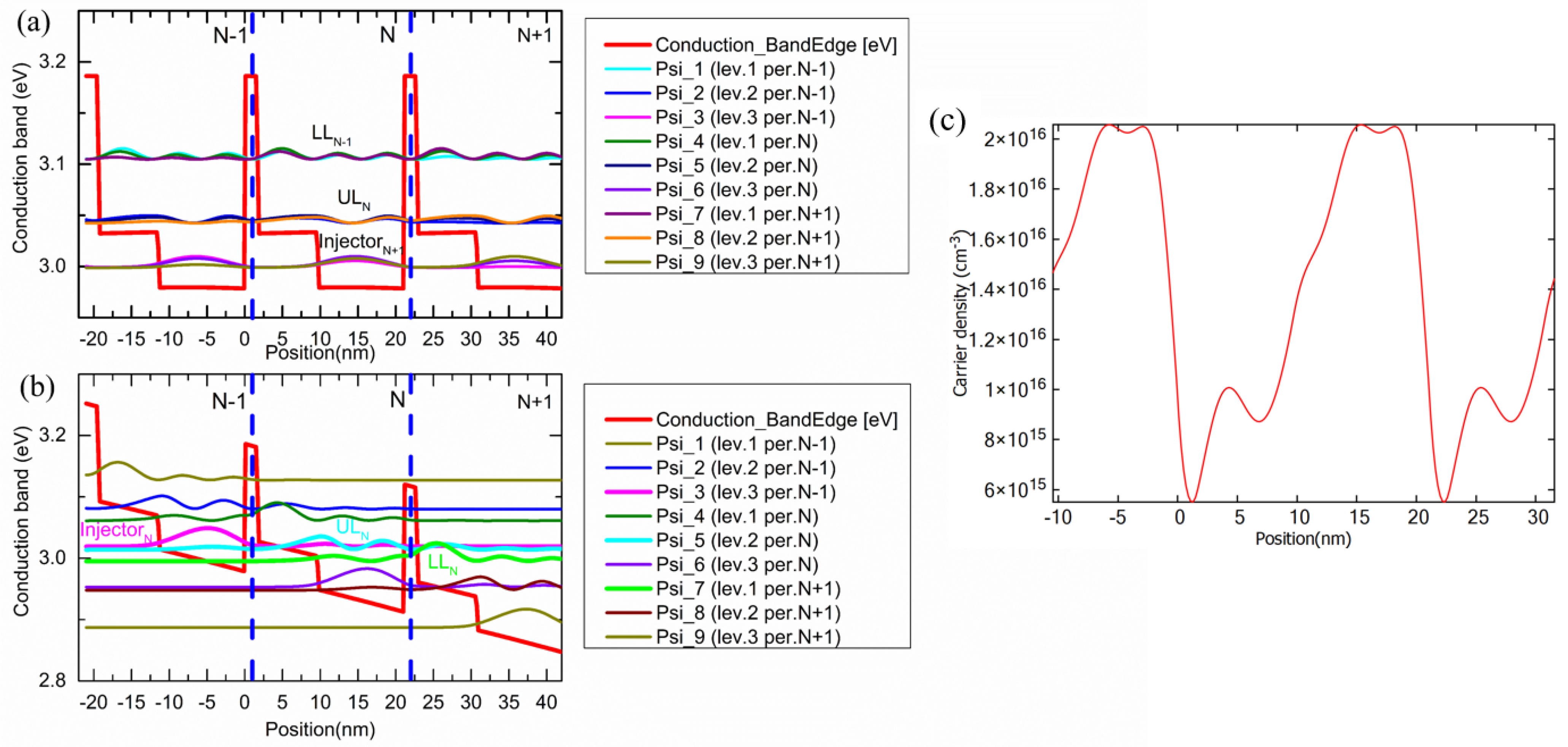
2. The Q1W Design Concept

A step-tapered barrier is used to combine the radiation barrier and injection barrier, and a three-level system is used in the Q1W design. A simplified concept diagram (Q1W test case 1) of the Q1W design with three main energy states is presented in Figure 1a. The diagram includes three repeating periods named per. N−1, per. N, and per. N+1, and there are only three layers per period.
Each period in Figure 1a,b is separated by a blue dashed line. From the left to the right of each period in Figure 1a,b, the first layer is a 1.7-nm-thick radiation barrier with 25% Al; the second layer is an 8-nm-thick step barrier layer with 7% Al; the third layer is an 11.4 nm GaAs-based quantum well. The start of the radiation barrier is set to be the zero position. Each period consists of an upper lasing state (UL), a lower lasing state (LL), and an injector/extractor state, but they do not contribute to the same electron transport and photon generation cycle within the same period at the design bias. Energy states in period N are labeled lev.1 per. N to lev.3 per. N from the highest energy to the lowest energy, shown in Figure 1a. In period N, the highest energy state (lev.1 per. N) will serve as LLn−1, the second-highest energy state (lev.2 per. N) will serve as ULn, and the lowest energy state (lev. 3 per. N) will serve as the injector staten+1 in the operation condition. Figure 1b shows the conduction band diagram at the design bias when the injectorn is lifted by the externally applied electric field and aligned with the ULn. The three main confined energy states in each period are named lev.1–3 in order of energy from the highest to the lowest in the same way as described in Figure 1a. The highest confined energy state in the N-th period (lev_1 per.N) serves as the LL for the (N−1)-th period, the second-highest confined energy state in the N-th period (lev_2 per.N) serves as the UL in the N-th period, and the lowest confined energy state in the N-th period (lev_3 per.N) serves as the injector/extractor state located around 43 meV below the LLn (lev_1 per.N+1) and aligns with ULn+1 (lev_2 per.N+1) in the subsequent period. The energy spacing between the injector/extractorn+1 state and the LLn state is ~7 meV higher than the LO phonon energy of ~36.5 meV for the purpose of reducing thermal back filling, the wrong extraction from UL, and possible absorption near the targeting lasing frequency. Moreover, it is worth noting that because LLn−1 is the higher energy state compared to ULn within the same period in the Q1W design scheme, it can enable faster re-injection of electrons from LLn−1 to ULn. In this case, M repeating periods would accommodate M−1 full pairs of lasing states, where M describes the number of repeating periods grown in AR. In other words, electrons can finish the cycle of injection-generating photon-collection every M/(M−1) well. Since a typical 10 µm THz QCL AR accommodates hundreds of repeating periods (M > 100), the average number of wells needed for one photon generation cycle is close to one. The thickness of one period in this design scheme is only ~20 nm, and it is narrower than any of the demonstrated THz QCL designs; therefore, an AR that is typically 10–13 µm [18] in thickness, which is set considering a proper tradeoff between reducing waveguide loss and maintaining a reasonable epitaxial growth time, can accommodate ~500 repeating periods (M = 500). The injection section that often contributes undesired negative optical gain in the THz frequency region is omitted in the Q1W design, and the required threshold population inversion between lasing states should therefore be lower due to the lower THz radiation re-absorption. Figure 1c shows the carrier distribution along two periods (from −10.45 nm to 31.55 nm) at the design bias. The trend and value of carrier distribution confirm the periodicity of the structure is well-preserved with field-periodic boundary conditions and a substantial population difference between the two sides of the radiation barrier is achieved.

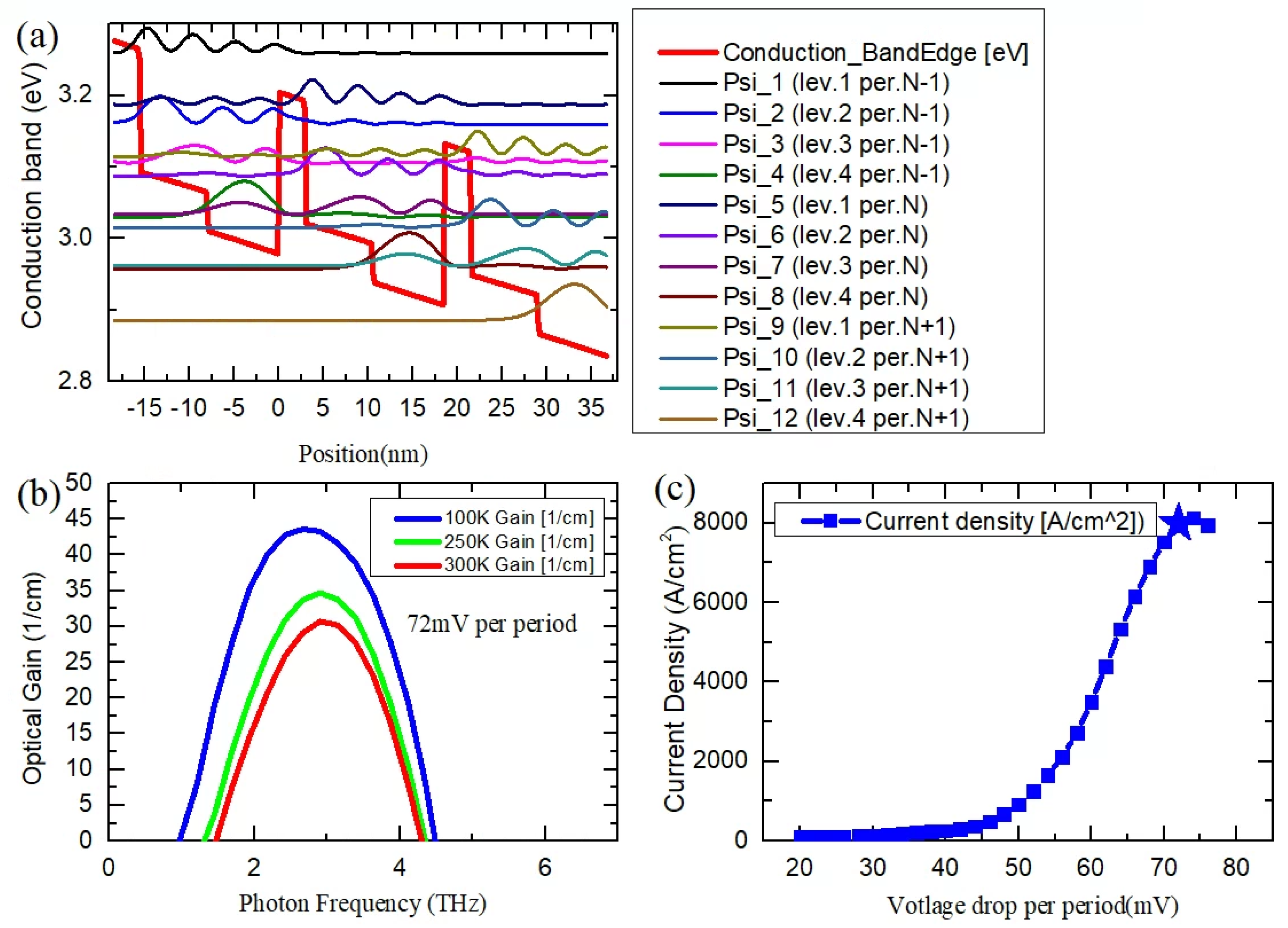
3. Development of the Q1W Design

The conduction band diagram of an actual design targeting an emission frequency of 3 THz is illustrated in Figure 2a. Figure 2b displays the simulated optical gain from 100 K to 300 K at a voltage of 72 mV per period. The simulation of optical gain is performed using the nextnano. NEGF simulation tool, which is a powerful and widely used tool in THz QCL simulations [39,40,41,42,43]. In the NEGF simulation tool, acoustic and optical phonon scattering, impurity scattering, IFR scattering, and alloy disorder scattering are accurately simulated by considering the full dependence of the scattered in-plane momentum. The three-band model is used to simulate nonparabolicity. Additionally, the electron–electron scattering is considered a self-consistent one-particle elastic approximation [43]. The NEGF simulation results show a sufficient optical gain of around 30/cm at 300 K. Figure 2c presents a simulated voltage–current density curve. Here, the maximum current density is observed at 74 mV/period. Note that the design bias is 72 mV/period, which is lower than the peak current bias (74 mV/period). This satisfies the pre-requisite of achieving population inversion in a PDR region.
A series of Q1W designs is summarized in Table 1, where the structure optimization parameter is the simulated optical gain. The simulation shows some absorption that is energetically centered around phonon energy and spatially overlapped lasing states (from the injectorn to the LLn, and from the ULn to the LLn−1). The designs, such as the Q1W-B, Q1W-C, Q1W-D, and Q1W-E, are among those that yield high optical gain. There are minor differences in the simulated optical gain using the NEGF model [35] and the RE model [33], which can be attributed to different material parameters (such as the AlxGa1−xAs bandgap [44,45] and interface roughness parameters) used in different model approaches. Nevertheless, both models show that Q1W designs (B, C, D, and E) could achieve better peak optical gain than those of G652 and V775 at 250 K. The Q1W-B shows the highest average optical gain calculated by the RE and nextnano. NEGF models. The Q1W-A and Q1W-C show the lowest operation bias compared to the other Q1W designs in Table 1. The Q1W-C2 has a lower doping density of 3 × 1010 cm−2, which can reduce the operating current density at the cost of a lower maximum optical gain. The Q1W-D is an optimization result based on RE with the band parameters from Wasilewski’s paper [44], while Q1W-E is an optimization result based on the nextnano. NEGF model with band parameters from Vurgraftman’s paper [35,45]. All of the Q1W designs exhibit higher operating electric fields in comparison to G652 and V775 as shown in Table 1. A higher operation current density and higher operation bias are some of the features of the Q1W design scheme. A high operation bias might cause high-joule heat and high over-barrier leakage. The over-barrier leakage and other characteristics of the Q1W-B are analyzed in the next section. A shorter pulse width, smaller device size, and higher thermal conductive substrate could be used to improve joule heat management.

4. Discussions Investigation of Temperature Sensitivity

The simulated optical gain versus temperature is simulated by the RE model and plotted to reveal the temperature dependence of the design performance, as shown in Figure 3a. In the RE model, the electron transitions are considered semi-classically within the period and as coherent tunneling between periods, and the two wells in the Q1W designs are treated as one calculation period. Three periods of each design are included in the calculation to estimate the electrons’ inter-period injection and extraction. The V775 [5] is shown in green, G652 [34] is in blue, and the simulated Q1W-B is shown as a red curve. The Q1W-B shows relatively weak temperature dependence—the optical gain drops slower as the temperature increases. The reason for the relatively lower temperature sensitivity in the Q1W-B is explained in Figure 3b. One of the major temperature-dependent performance degradation factors for THz QCLs is thermally activated LO phonon scattering. Hot electrons with high kinetic energy can be scattered from UL to LL via phonon emission. This LO phonon scattering at high temperature dominates scattering mechanisms between UL and LL, so the population inversion is substantially reduced or even completely lost at higher temperatures. However, only in the Q1W designs, LLn is the third lowest energy state and ULn+1 is the second lowest energy state in the same well, as described in Figure 1a. Hence, the overlap between LLn and ULn+1 is large, and electrons tend to scatter to the lower energy state in the same well. In other words, the scattering time from LLn to ULn+1 (dashed line in Figure 3b) is faster than the LO phonon scattering between diagonally spaced ULn to LLn (solid line in Figure 3b) in the temperature range of 30–290 K, as shown in Figure 3b. The dominant electron scattering process is from LLn to ULn+1. The fast scattering may introduce extra broadening to lasing states and thus results in the lower peak optical gain observed compared to V652 and V775 at temperatures lower than ~150 K, as shown in Figure 3a. More importantly, this scattering process from LLn to ULn+1 can compensate for the detrimental LO phonon scattering from ULn to LLn and help keep the population inversion from fast temperature-dependent degradation at high temperatures.
The temperature-dependent over-barrier leakage current is also calculated and compared between the Q1W-B and state-of-the-art designs shown in Figure 3c. Despite the higher operation bias of the Q1W design, the leakage current to the continuum is limited below 500 A/cm2 in the Q1W-B and G652. For comparison, the V775 shows a much higher leakage current to the continuum than the Q1W-B, as shown in Figure 3c. This simulation result indicates that over-barrier leakage might not be a significant issue in the Q1W design.

5. Critical Design Parameters

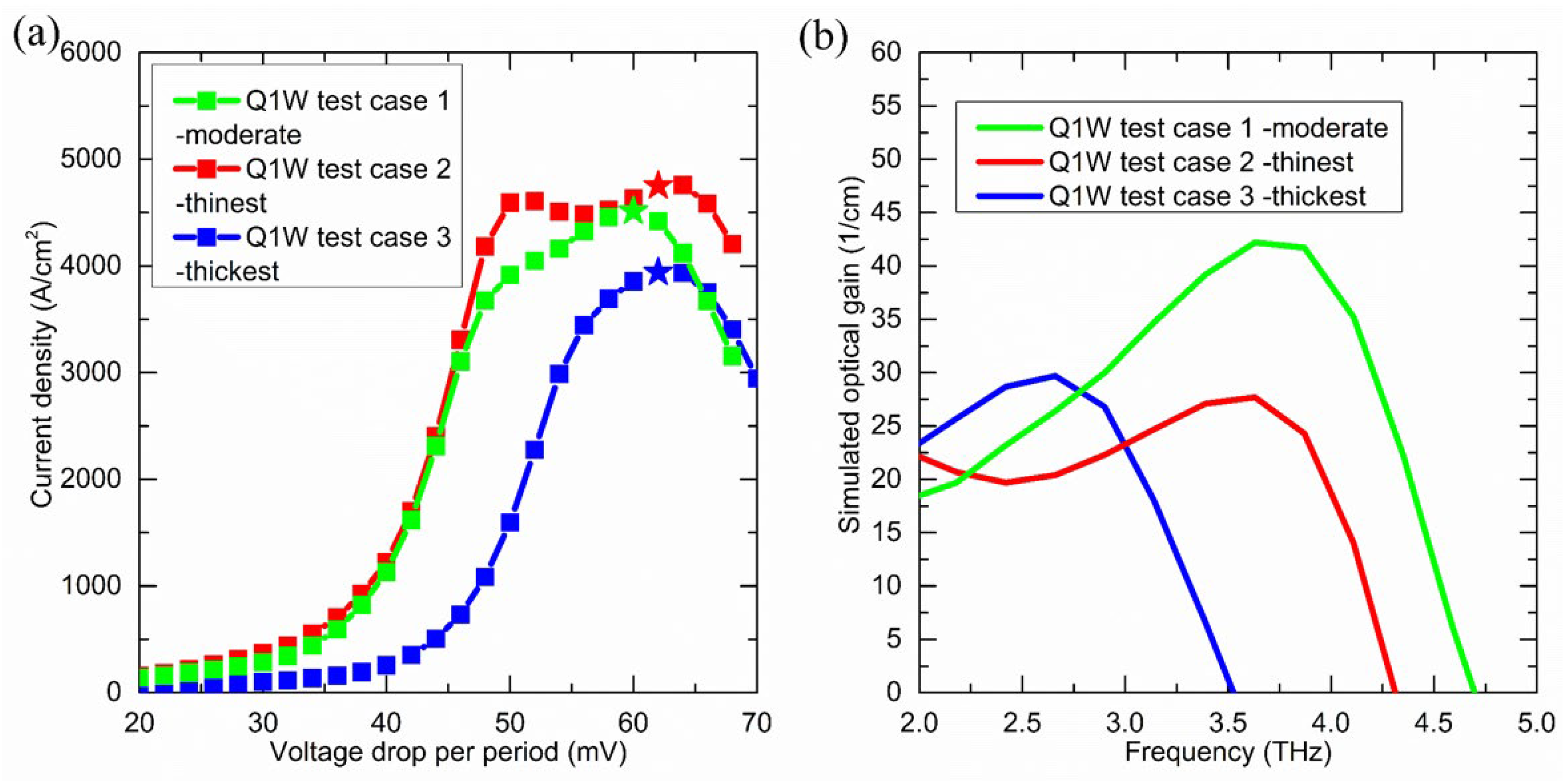
5.1. Effect of Step-Tapered Barrier Thickness

The step-tapered barrier affects both the current density–voltage (JV) curve and optical gain, and the effect is discussed in this section. The JV curves and calculated optical gain of three test cases are presented in Figure 4. JV curves are important simulation results to assess if the Q1W design can achieve design bias before entering the NDR. THz QCLs at the design bias usually exhibit the highest population inversion and optical gain, and it is important to ensure that a sufficiently high optical gain is achieved in the PDR region [37]. The step-tapered barrier plays a critical role in tuning JV curves, avoiding the design bias to be in an NDR region, achieving sufficient optical gain, and ultimately leading to lasing operation.
An example of how step-tapered barrier thicknesses affect the simulation performance with three main energy states is presented in Figure 4. In the simplified three-level simulation, all three test cases (test cases 1–3) reveal that the highest optical gain is achieved at the electric bias with the highest current density (marked by stars on the JV curves). Test case 1 is the optimized structure using the simplified three-level simulation as shown in Figure 1, and its barrier is 9.7 nm thick, which consists of a 1.7-nm-thick Al0.25Ga0.75As-based radiation barrier and an 8-nm-thick Al0.07Ga0.93As-based step barrier. The GaAs-based quantum well is 11.4 nm thick. Test case 1 shows a peak current density of ~4500 A/cm2 at a bias of 60 mV per period in the NEGF model. The peak gain achieved without considering leakage levels is 48/cm at 100 K.
Test case 2 presents the structure with a step-tapered barrier that is 1 nm thinner than test case 1, and test case 3 presents the structure with a step-tapered barrier that is 1 nm thicker than test case 1. The quantum well thickness of test case 3 is also tuned to be 1 nm thinner than test cases 1 and 2 to keep the energy spacing between lasing states close to 3 THz. The normal variation during the growth is typically less than 1 nm.
The results of test cases 1 to 3 reveal the effect of the step-tapered barrier on the JV curve and optical gain. On one hand, the barrier needs to be thick enough to keep the pre-threshold leakage channels sufficiently low to ensure the peak gain is achieved in the PDR region. The step-tapered barrier, which is 1.7 (25%Al)/7 (7%Al) in test case 2, is close to the thinnest barrier it can be to ensure a threshold bias in PDR, because the pre-threshold leakage channel at the voltage of 50 mV per period produces almost the same amount of current as in the design bias of 62 mV per period as shown in Figure 4a. On the other hand, increasing the barrier thickness leads to reduced injection coupling energy, thus lowering the maximum population inversion that can be achieved. A thicker barrier, which is 2.7 (25%Al)/7 (7%Al), in test case 3 reduces the peak gain from 48/cm to ~26/cm at 100 K. Substantial optimizations are needed to identify the sweet point of the step-tapered barrier thickness. The barrier thickness in this section is tested under the condition of a well width of 10.4–11.4 nm. The well width should be adjusted according to the barrier thickness and height due to the position and energy change of confined states. However, the effect of the step-tapered barrier thickness follows the trend discussed in this section.

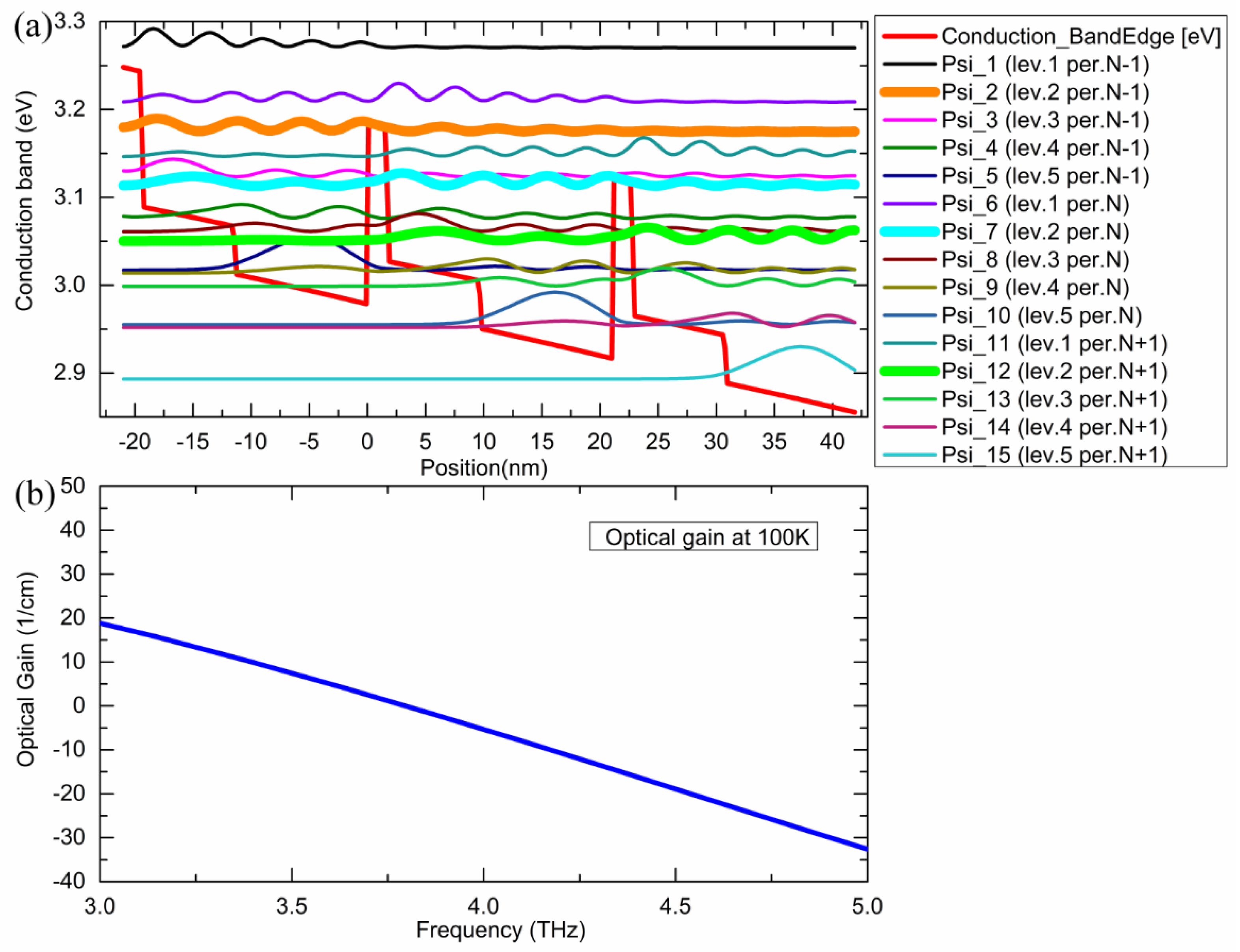
5.2. Effect of High-Energy Parasitic Energy Levels

The principle of the Q1W design scheme is initially verified by a simplified three-level simulation. In order to investigate parasitic energy levels in the Q1W designs, a full simulation with all confined energy states with energy up to the barrier edge for each period is performed. It is worth noting that the second-highest energy state (highlighted by thick lines) in the (N+1)-th period is closely spaced in energy with UL (lev.4 per.N in Figure 5a) in the N-th period. Due to the short period, the two energy states can be strongly coupled at the alignment condition near the design bias, as described in Figure 5a. This strong coupling can create a leakage path that vanishes the gain of test case 1 at 100 K. Around 15% of available electrons remain on the leakage level and the optical gain peak vanished at 3.75 THz from a high value shown in Figure 4b to the low value shown in Figure 5b.
The GaAs well width plays a key role in tuning the parasitic energy levels in the Q1W design, as a thinner quantum well will push confined energy states to higher energy and achieve larger energy spacing. After having performed a large number of trials for this design, we found a good choice for the Q1W thickness, which is shown in Figure 2, and successfully tuned the first parasitic channel to energy higher than UL and thus reduced the coupling strength, which can alleviate the leakage issue and retain the design bias in the PDR region. The step-tapered barrier is also adjusted in accordance with the change of the well width. In the actual design, shown in Figure 2, the parasitic energy level still creates a leakage current, but not so significant as to ruin the population inversion. The optical gain is improved, as shown in Figure 2b, by tuning the parasitic energy level.

6. Conclusions

In conclusion, the Q1W scheme is presented theoretically using the nextnano. NEGF model [35] and the RE model [33]. The Q1W design series consists of only three layers per period, and the total thickness per period is below 20 nm, which is considered thinner than any of the previously demonstrated THz QCL designs. The Q1W design series exhibits a sufficient positive peak gain of ~35/cm at 250 K at a design electric field of ~35–39 kV/cm. The design bias is located in a PDR region with a peak current density of 4–8 kA/cm2. These features of the Q1W design scheme make it a promising THz QCL design scheme for high-efficiency and high-temperature performance.

Author Contributions

Conceptualization, B.W.; methodology, B.W.; software, B.W.; validation, B.W. and D.B.; formal analysis, B.W.; investigation, B.W.; resources, D.B.; data curation, B.W.; writing—original draft preparation, B.W.; writing—review and editing, D.B.; visualization, B.W. and D.B.; supervision, D.B.; project administration, D.B.; funding acquisition, D.B. All authors have read and agreed to the published version of the manuscript.

Funding

This research was supported by the Natural Sciences and Engineering Research Council of Canada (NSERC) and Ontario Centres for Excellence (OCE), Canada.

Acknowledgments

The author would like to acknowledge Thomas Grange for allowing the use of nextnano. NEGF in this paper. The NEGF model simulation results in this paper are produced by nextnano. NEGF.

Conflicts of Interest

The authors declare no conflict of interest.

References

  1. Köhler, R.; Tredicucci, A.; Beltram, F.; Beere, H.E.; Linfield, E.H.; Davies, A.G.; Ritchie, D.A.; Iotti, R.C.; Rossi, F. Terahertz semiconductor-heterostructure laser. Nature 2002, 417, 156–159. [Google Scholar] [CrossRef] [PubMed]
  2. Bosco, L.; Franckié, M.; Scalari, G.; Beck, M.; Wacker, A.; Faist, J. Thermoelectrically cooled THz quantum cascade laser operating up to 210 K. Appl. Phys. Lett. 2019, 115, 010601. [Google Scholar] [CrossRef]
  3. Williams, B.S. Terahertz quantum-cascade lasers. Nat. Photonics 2007, 1, 517–525. [Google Scholar] [CrossRef] [Green Version]
  4. Kumar, S.; Chan, C.W.I.; Hu, Q.; Reno, J.L. A 1.8-THz quantum cascade laser operating significantly above the temperature of ℏ ω/k B. Nat. Phys. 2011, 7, 166–171. [Google Scholar] [CrossRef]
  5. Fathololoumi, S.; Dupont, E.; Chan, C.; Wasilewski, Z.; Laframboise, S.; Ban, D.; Mátyás, A.; Jirauschek, C.; Hu, Q.; Liu, H. Terahertz quantum cascade lasers operating up to ∼200 K with optimized oscillator strength and improved injection tunneling. Opt. Express 2012, 20, 3866–3876. [Google Scholar] [CrossRef]
  6. Scalari, G.; Ajili, L.; Faist, J.; Beere, H.; Linfield, E.; Ritchie, D.; Davies, G. Far-infrared (λ = 87 μm) bound-to-continuum quantum-cascade lasers operating up to 90 K. Appl. Phys. Lett. 2003, 82, 3165–3167. [Google Scholar] [CrossRef]
  7. Scalari, G.; Hoyler, N.; Giovannini, M.; Faist, J. Terahertz bound-to-continuum quantum-cascade lasers based on optical-phonon scattering extraction. Appl. Phys. Lett. 2005, 86, 181101. [Google Scholar] [CrossRef]
  8. Vitiello, M.S.; Scamarcio, G.; Spagnolo, V.; Dhillon, S.S.; Sirtori, C. Terahertz quantum cascade lasers with large wall-plug efficiency. Appl. Phys. Lett. 2007, 90, 191115. [Google Scholar] [CrossRef]
  9. Albo, A.; Flores, Y.V.; Hu, Q.; Reno, J.L. Two-well terahertz quantum cascade lasers with suppressed carrier leakage. Appl. Phys. Lett. 2017, 111, 111107. [Google Scholar] [CrossRef]
  10. Liu, J.; Chen, J.; Wang, T.; Li, Y.; Liu, F.; Li, L.; Wang, L.; Wang, Z. High efficiency and high power continuous-wave semiconductor terahertz lasers at ∼3.1 THz. Solid-State Electron. 2013, 81, 68–71. [Google Scholar] [CrossRef]
  11. Freeman, J.R.; Brewer, A.; Madéo, J.; Cavalié, P.; Dhillon, S.S.; Tignon, J.; Beere, H.E.; Ritchie, D.A. Broad gain in a bound-to-continuum quantum cascade laser with heterogeneous active region. Appl. Phys. Lett. 2011, 99, 241108. [Google Scholar] [CrossRef]
  12. Amanti, M.I.; Scalari, G.; Terazzi, R.; Fischer, M.; Beck, M.; Faist, J.; Rudra, A.; Gallo, P.; Kapon, E. Bound-to-continuum terahertz quantum cascade laser with a single-quantum-well phonon extraction/injection stage. New J. Phys. 2009, 11, 125022. [Google Scholar] [CrossRef]
  13. Schrottke, L.; Lü, X.; Rozas, G.; Biermann, K.; Grahn, H.T. Terahertz GaAs/AlAs quantum-cascade lasers. Appl. Phys. Lett. 2016, 108, 102102. [Google Scholar] [CrossRef]
  14. Deutsch, C.; Detz, H.; Krall, M.; Brandstetter, M.; Zederbauer, T.; Andrews, A.; Schrenk, W.; Strasser, G.; Unterrainer, K. Dopant migration effects in terahertz quantum cascade lasers. Appl. Phys. Lett. 2013, 102, 201102. [Google Scholar] [CrossRef]
  15. Chassagneux, Y.; Wang, Q.; Khanna, S.; Strupiechonski, E.; Coudevylle, J.-R.; Linfield, E.; Davies, A.; Capasso, F.; Belkin, M.; Colombelli, R. Limiting factors to the temperature performance of THz quantum cascade lasers based on the resonant-phonon depopulation scheme. IEEE Trans. Terahertz Sci. Technol. 2011, 2, 83–92. [Google Scholar] [CrossRef]
  16. Sirtori, C.; Barbieri, S.; Colombelli, R. Wave engineering with THz quantum cascade lasers. Nat. Photonics 2013, 7, 691–701. [Google Scholar] [CrossRef]
  17. Walther, C.; Fischer, M.; Scalari, G.; Terazzi, R.; Hoyler, N.; Faist, J. Quantum cascade lasers operating from 1.2 to 1.6 THz. Appl. Phys. Lett. 2007, 91, 131122. [Google Scholar] [CrossRef]
  18. Wen, B.; Ban, D. High-temperature Terahertz Quantum Cascade Lasers. Prog. Quantum Electron. 2021, 80, 100363. [Google Scholar] [CrossRef]
  19. Baranov, A.; Nguyen-Van, H.; Loghmari, Z.; Bahriz, M.; Teissier, R. Terahertz quantum cascade laser with non-resonant extraction. AIP Adv. 2019, 9, 055214. [Google Scholar] [CrossRef]
  20. Kainz, M.A.; Schönhuber, S.; Andrews, A.M.; Detz, H.; Limbacher, B.; Strasser, G.; Unterrainer, K. Barrier height tuning of terahertz quantum cascade lasers for high-temperature operation. ACS Photonics 2018, 5, 4687–4693. [Google Scholar] [CrossRef]
  21. Luo, H.; Laframboise, S.; Wasilewski, Z.; Aers, G.; Liu, H.; Cao, J. Terahertz quantum-cascade lasers based on a three-well active module. Appl. Phys. Lett. 2007, 90, 041112. [Google Scholar] [CrossRef]
  22. Wen, B.; Xu, C.; Wang, S.; Wang, K.; Tam, M.C.; Wasilewski, Z.; Ban, D. Dual-lasing channel quantum cascade laser based on scattering-assisted injection design. Opt. Express 2018, 26, 9194–9204. [Google Scholar] [CrossRef] [PubMed]
  23. Dupont, E.; Fathololoumi, S.; Wasilewski, Z.; Aers, G.; Laframboise, S.; Lindskog, M.; Razavipour, S.; Wacker, A.; Ban, D.; Liu, H. A phonon scattering assisted injection and extraction based terahertz quantum cascade laser. J. Appl. Phys. 2012, 111, 073111. [Google Scholar] [CrossRef] [Green Version]
  24. Razavipour, S.; Dupont, E.; Chan, C.; Xu, C.; Wasilewski, Z.; Laframboise, S.; Hu, Q.; Ban, D. A high carrier injection terahertz quantum cascade laser based on indirectly pumped scheme. Appl. Phys. Lett. 2014, 104, 041111. [Google Scholar] [CrossRef]
  25. Razavipour, S.G.; Dupont, E.; Fathololoumi, S.; Chan, C.; Lindskog, M.; Wasilewski, Z.; Aers, G.; Laframboise, S.; Wacker, A.; Hu, Q. An indirectly pumped terahertz quantum cascade laser with low injection coupling strength operating above 150 K. J. Appl. Phys. 2013, 113, 203107. [Google Scholar] [CrossRef]
  26. Franckié, M.; Bosco, L.; Beck, M.; Bonzon, C.; Mavrona, E.; Scalari, G.; Wacker, A.; Faist, J. Two-well quantum cascade laser optimization by non-equilibrium Green’s function modelling. Appl. Phys. Lett. 2018, 112, 021104. [Google Scholar] [CrossRef] [Green Version]
  27. Scalari, G.; Amanti, M.; Walther, C.; Terazzi, R.; Beck, M.; Faist, J. Broadband THz lasing from a photon-phonon quantum cascade structure. Opt. Express 2010, 18, 8043–8052. [Google Scholar] [CrossRef]
  28. Albo, A.; Flores, Y.V.; Hu, Q.; Reno, J.L. Split-well direct-phonon terahertz quantum cascade lasers. Appl. Phys. Lett. 2019, 114, 191102. [Google Scholar] [CrossRef] [Green Version]
  29. Freeman, W. Longitudinal-optical phonon absorption and dephasing in three-level terahertz quantum cascade structures with different injector anticrossings. J. Appl. Phys. 2020, 128, 235702. [Google Scholar] [CrossRef]
  30. Wacker, A. Extraction-controlled quantum cascade lasers. Appl. Phys. Lett. 2010, 97, 081105. [Google Scholar] [CrossRef] [Green Version]
  31. Han, Y.; Li, L.; Grier, A.; Chen, L.; Valavanis, A.; Zhu, J.; Freeman, J.; Isac, N.; Colombelli, R.; Dean, P. Extraction-controlled terahertz frequency quantum cascade lasers with a diagonal LO-phonon extraction and injection stage. Opt. Express 2016, 24, 28583–28593. [Google Scholar] [CrossRef] [PubMed] [Green Version]
  32. Wen, B.; Deimert, C.; Wang, S.; Xu, C.; Rassel, S.S.; Wasilewski, Z.; Ban, D. Six-level hybrid extraction/injection scheme terahertz quantum cascade laser with suppressed thermally activated carrier leakage. Opt. Express 2020, 28, 26499–26508. [Google Scholar] [CrossRef] [PubMed]
  33. Cooper, J.; Valavanis, A.; Ikonić, Z.; Harrison, P.; Cunningham, J. Finite difference method for solving the Schrödinger equation with band nonparabolicity in mid-infrared quantum cascade lasers. J. Appl. Phys. 2010, 108, 113109. [Google Scholar] [CrossRef]
  34. Khalatpour, A.; Paulsen, A.K.; Deimert, C.; Wasilewski, Z.R.; Hu, Q. High-power portable terahertz laser systems. Nat. Photonics 2021, 15, 16–20. [Google Scholar] [CrossRef]
  35. The nextnano.NEGF Software for Quantum Transport. Available online: https://nextnano-docu.northeurope.cloudapp.azure.com/dokuwiki/doku.php?id=negf:the_nextnano.negf_software (accessed on 6 October 2020).
  36. Sekine, N.; Hirakawa, K. Dispersive terahertz gain of a nonclassical oscillator: Bloch oscillation in semiconductor superlattices. Phys. Rev. Lett. 2005, 94, 057408. [Google Scholar] [CrossRef]
  37. Winge, D.O.; Dupont, E.; Wacker, A. Ignition of quantum cascade lasers in a state of oscillating electric field domains. Phys. Rev. A 2018, 98, 023834. [Google Scholar] [CrossRef] [Green Version]
  38. Winge, D.O.; Franckié, M.; Wacker, A. Superlattice gain in positive differential conductivity region. AIP Adv. 2016, 6, 045025. [Google Scholar] [CrossRef] [Green Version]
  39. Gower, N.L.; Piperno, S.; Albo, A. Comparison of THz-QCL Designs Supporting Clean N-Level Systems. Photonics 2021, 8, 248. [Google Scholar] [CrossRef]
  40. Wang, L.; Lin, T.-T.; Wang, K.; Grange, T.; Birner, S.; Hirayama, H. Short-period scattering-assisted terahertz quantum cascade lasers operating at high temperatures. Sci. Rep. 2019, 9, 9446. [Google Scholar] [CrossRef]
  41. Jirauschek, C.; Kubis, T. Modeling techniques for quantum cascade lasers. Appl. Phys. Rev. 2014, 1, 011307. [Google Scholar] [CrossRef] [Green Version]
  42. Grange, T. Contrasting influence of charged impurities on transport and gain in terahertz quantum cascade lasers. Phys. Rev. B 2015, 92, 241306. [Google Scholar] [CrossRef] [Green Version]
  43. Grange, T.; Stark, D.; Scalari, G.; Faist, J.; Persichetti, L.; di Gaspare, L.; de Seta, M.; Ortolani, M.; Paul, D.J.; Capellini, G. Room temperature operation of n-type Ge/SiGe terahertz quantum cascade lasers predicted by non-equilibrium Green’s functions. Appl. Phys. Lett. 2019, 114, 111102. [Google Scholar] [CrossRef] [Green Version]
  44. Wasilewski, Z.; Dion, M.; Lockwood, D.; Poole, P.; Streater, R.; Spring Thorpe, A. Composition of AlGaAs. J. Appl. Phys. 1997, 81, 1683–1694. [Google Scholar] [CrossRef]
  45. Zawadzki, W.; Pfeffer, P. Spin splitting of subband energies due to inversion asymmetry in semiconductor heterostructures. Semicond. Sci. Technol. 2003, 19, R1. [Google Scholar] [CrossRef]
Figure 1. Conduction band diagram and carrier distribution at 100 K. (a) Concept conduction band diagram of a Q1W design (1.7 nm Al0.25Ga0.75As/8 nm Al0.07Ga0.93As/11.4 nm GaAs) at zero bias. (b) Conduction band diagram of a Q1W design at a design bias of 72 mV per period. (c) Carrier distribution along two periods from −10.45 nm to 31.55 nm.
Photonics 09 00247 g001
Figure 2. Q1W-B (3.0 nm Al0.27Ga0.73As/7.5 nm Al0.07Ga0.93As/8 nm GaAs) simulation result by NEGF model. (a) Conduction band diagram. (b) Calculated temperature-dependent optical gain. (c) Voltage–current density curve at 100 K. NEGF simulation is performed by using the nextnano. NEGF simulation tool from [35].
Photonics 09 00247 g002
Figure 3. Temperature-dependent calculations via RE model. (a) Temperature-dependent optical gain, (b) LO phonon scattering time from ULn to LLn (solid line) and scattering time from LLn to ULn+1 (dashed line), and (c) over-barrier leakage current based on RE model. Blue curve is two-well DP structure G652, green curve is RP structure V775, and red curve is the Q1W-B.
Photonics 09 00247 g003
Figure 4. Simulation performance of three Q1W designs at 100 K. (a) JV curves at 100 K. (b) Optical gain at 100 K. Test case 1: 1.7 (25%Al)/8 (7%Al)/11.4 (GaAs), test case 2: 1.7 (25%Al)/7 (7%Al)/11.4 (GaAs), test case 3: 2.7 (25%Al)/7 (7%Al)/10.4 (GaAs). Layer thickness is shown in nm, and numbers in bold indicate barriers. The underlined layers are averagely doped to achieve sheet density of 3 × 1010 cm−2. Test cases 1–3 failed during subsequent investigation conducted in the next section, which studies high-energy parasitic energy levels.
Photonics 09 00247 g004
Figure 5. Effect of a parasitic energy level. (a) Conduction band diagram of the Q1W test case 2 at 62 mV per period. (b) Calculated optical gain of test case 2 with high energy leakage levels at 100 K.
Photonics 09 00247 g005
Table 1. Summary of optimized designs. Design A: 3.0 (27%Al)/8 (7%Al)/8.7 (GaAs). Design B: 3.0 (27%Al)/7.5 (7%Al)/8.0 (GaAs). Design C: 3.0 (25%Al)/8 (7%Al)/8.7 (GaAs). Design D: 3.0 (27%Al)/8.3 (5%Al)/7.5 (GaAs). Design E: 3.0 (30%Al)/7.5 (7%Al)/8.0 (GaAs). Layer thicknesses are shown in nm. The underlined layers are averagely doped. The operation bias and electric field are calculated by nextnano. NEGF model.
DesignNEGF Simulated Peak Optical Gain @ 250 K
(cm−1)
RE Simulated Peak Optical Gain @ 250 K
(cm−1)
Operation Bias
(mV/Period)
Sheet Doping Density
(cm−1)
Period Length
(nm)
Electric Field
(kV/cm)
Q1W-A28.316.0684.5 × 101019.734.5
Q1W-B34.729.8724.5 × 101018.538.9
Q1W-C32.724.6684.5 × 101019.734.5
Q1W-C222.016.4683 × 101019.734.5
Q1W-D28.131664.5 × 101018.835.1
Q1W-E3521.9724.5 × 101018.538.9
G652 [34]16.519.0764.03 × 101026.928.2
V775 [5]15.16.42583.0 × 101043.9113.3
Publisher’s Note: MDPI stays neutral with regard to jurisdictional claims in published maps and institutional affiliations.

