1. Introduction
The quantum cascade laser (QCL) has been demonstrated to be an extremely versatile, chip-scale source of mid-infrared to THZ light at room temperature. At present, high power, wavelength tuning, and frequency comb operation have all been realized [
1,
2,
3], which are beneficial traits for a wide range of systems, including infrared countermeasures, free space communications, and chemical/biological detection [
4,
5,
6]. Two aspects of the technology that are currently being explored are mass production and massively parallel integration, in order to reduce discrete device cost and facilitate system-on-a-chip implementation. These aspects would be most easily realized if the QCL could be integrated directly on large-diameter (up to 450 mm) Si wafers, but device performance should be on par with existing commercial products. These wafers are relatively inexpensive, and can be used directly with the highest quality and highest throughput fabrication equipment.
Hybrid integration of QCL wafers via wafer bonding to Si is one option, and has been explored by multiple groups [
7]. This approach is not easily scalable, though, as commercial InP wafers have a maximum diameter of 150 mm. Multiple wafers would be required to cover the whole Si wafer, and there would be a low fill factor. Direct bonding of QCLs onto Si waveguides is another option, but requires individual device alignment with submicron accuracy. This is also not easily scalable to large wafers.
A potentially simpler solution is the direct epitaxial growth of QCLs on the desired photonics platform. The primary challenge in this case is maintaining the crystalline quality and sharp interfaces of the QCL in the presence of lattice constant and/or thermal expansion mismatch. The highest performance mid-infrared (3 < λ < 5 μm) QCLs are based on InP, which is the same platform used for most 1.3–1.55 μm diode lasers that are used for telecommunication. Si has an 8% lattice constant mismatch with respect to InP, which has been a significant technical hurdle to overcome. Nevertheless, various solutions to realizing 1.3–1.55 μm lasers on Si through direct growth have been realized [
8,
9]. Though working devices have been achieved, the performance is generally inferior to lasers grown on native substrates due to the presence of dislocations, which can act as non-radiative recombination centers and potential failure points.
Unlike the traditional diode laser, the QCL is a majority carrier device that relies on intersubband electron transitions for transport and light emission. This means that dislocations have a very different impact on device operation. Rather than non-radiative recombination centers, dislocations primarily affect carrier concentration and mobility. As a result, the impact on gain and/or carrier lifetime is not expected to be as severe as for a traditional laser diode.
Structural challenges do still exist, however. The QCL is composed of hundreds of layers with a well-defined, monolayer-scale thickness. Intersubband gain can only be realized if the layer thicknesses and compositions can be maintained, which requires flat regions of good crystal quality. This can be difficult to realize in a mismatched system due to the possibility of 3D growth modes, especially during relaxation of compressively strained films (such as InP on Si).
Though growth of InP-based QCLs on Si is the eventual goal, an intermediate step is to grow them first on GaAs, which has approximately half the lattice mismatch (4%). This has been attempted by several groups in the past. The most recent attempt achieved room temperature operation, but with only ~12 mW of peak power at an input current of 4.4 A [
10]. This is far below the state-of-the-art for QCLs on native substrates.
In this paper, through growth of a high-quality metamorphic buffer layer and QCL structure, QCLs on GaAs are demonstrated with multi-watt power output, which is approximately 3 orders of magnitude higher than any previous demonstration of this type of device.
2. Materials and Methods
The experiment starts with the growth of a metamorphic InP layer directly on an n+ GaAs wafer using low-pressure metalorganic chemical vapor deposition (LP-MOCVD). A 100 nm thick n-GaAs buffer layer is first grown at a temperature of 560 °C using TMGa, dilute SiH4, and AsH3 as precursors. The growth temperature is then lowered to 400 °C under AsH3. An abrupt transition is made to n-InP, which is grown using TMIn, dilute SiH4, and PH3. After ~100 nm of low-temperature InP growth, the temperature is then increased to 580 °C, where an additional 3.1 μm of n-InP is grown. All steps were performed with a pressure setpoint of 60 Torr. No graded composition buffer layer was incorporated.
Growth of the active QCL layers was achieved using gas-source molecular beam epitaxy (GSMBE). The band structure of the QCL gain medium is based on the shallow-well design in [
11]. Identical layer sequences and environmental conditions are used for growth of a 40-stage, mid-infrared high-efficiency laser core on the InP-coated GaAs template described above. Below the laser core, an 800 nm thick n-InP layer is grown in order to help improve the starting surface for the QCL active layers. On top of the laser core, a 100 nm thick n-InP layer is grown, followed by 300 nm thick n-GaInAs and a 20 nm thick n-InP cap layer. Following GSMBE growth, a 3 μm thick n-InP cladding layer and a 1 μm thick n
+ InP cap layer are grown on pieces of both wafers using LP-MOCVD.
Once wafer growth was complete, a piece was fabricated into double channel waveguide QCLs. This simple process used wet etching to define a central waveguide of 25 μm width. Insulation of the waveguide was achieved with a 750 nm thick layer of SiO
2. A 5 μm wide window was etched through the SiO
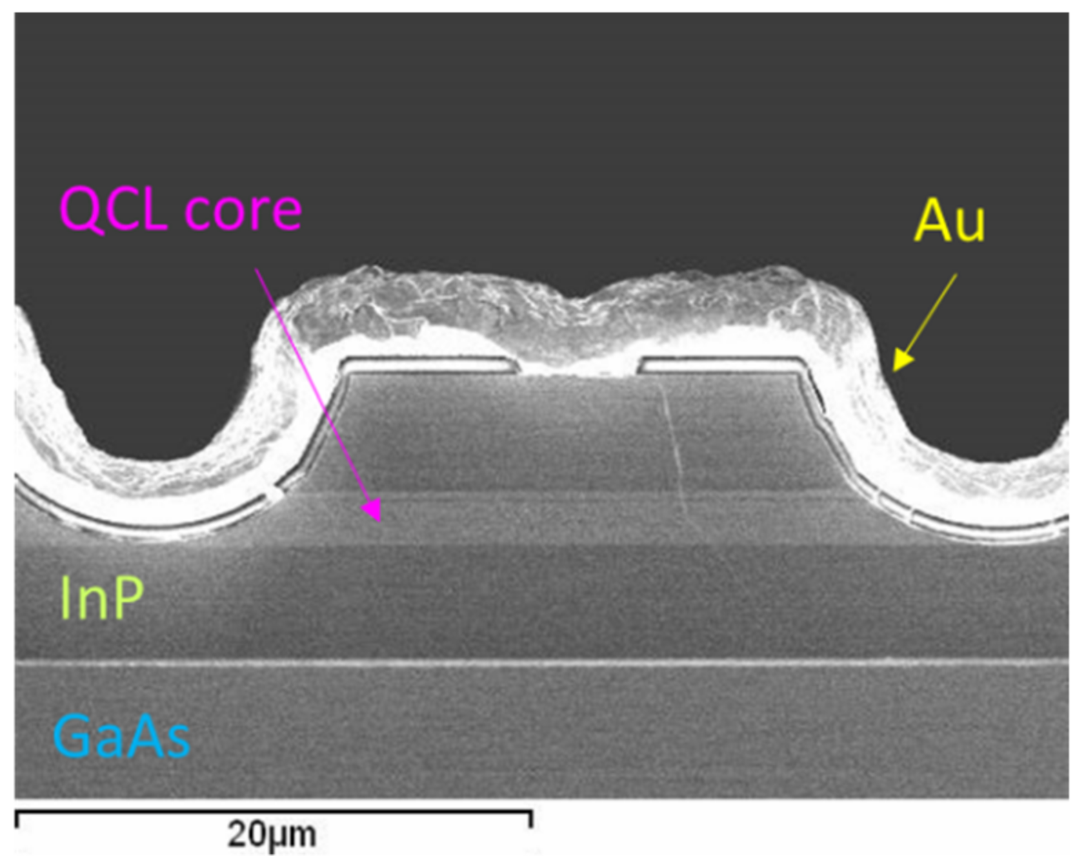
2 on top of the waveguide for current injection. Ti/Au was used as a top metal contact, followed by electroplating of ~2 μm of Au. The backside of the wafers was then thinned to ~200 μm and polished. A AuGe/Ni/Au multilayer was used to make an ohmic bottom contact to the n+ GaAs polished surface. The process was finished with a short anneal at 370 °C to improve metal adhesion. A cross-section of a cleaved laser facet is shown in
Figure 1. A clear demarcation between the GaAs substrate and InP buffer is observed, but the cleaved laser facet is generally smooth near the laser core.
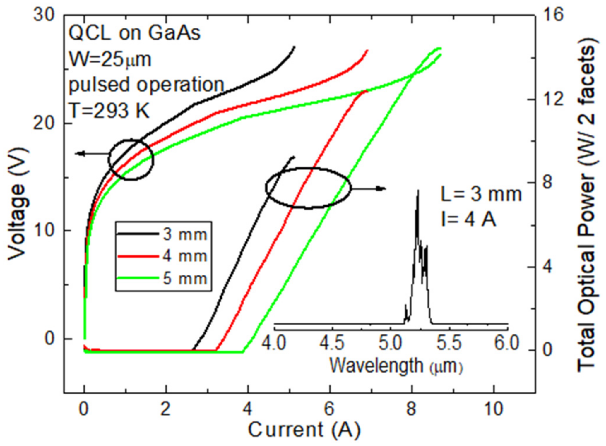
For testing, laser bars of 3, 4, and 5 mm were cleaved, and the mirror facets were left uncoated. Laser bars were mounted epilayer-up with indium to copper heat sinks. Laser testing was conducted in pulsed mode using 200 ns pulses at a repetition rate of 100 kHz. The heat sink temperature was regulated by a thermistor and a thermoelectric cooler. Average power is measured by a calibrated thermopile detector placed in close proximity to the front laser facet. Peak power is calculated by dividing average power by the pulsed duty cycle (0.02). Total power from both mirror facets is calculated by multiplying the measured power by 2. Spectral measurements are also conducted in pulsed mode, using a high-resolution (0.125 cm−1) Bruker IFS 66v/S FTIR and a deuterated triglycine sulfate (DTGS) detector.
3. Results
3.1. Material Characterization of Wafer
The InP-coated GaAs template was characterized using optical and atomic force microscopy (AFM). The rms roughness of the surface after template growth was only 1.2 nm over a 10 μm × 10 μm area. After growth of the QCL laser core, cladding, and cap layer, the rms roughness is maintained below 2 nm rms, with flat regions of several μm2 observed.
The QCL on GaAs was measured using high-resolution X-ray diffraction and does not show distinct satellite peaks, as can be expected from the measured surface roughness. However, when compared with a similar structure grown directly on InP, the overall features of the diffraction envelope are reproduced, along with a clear GaAs substrate peak (
Figure 2a). This indicates that the overall superlattice structure is maintained, despite the large lattice mismatch.
For electrical characterization, the doping profile was measured as a function of depth using electrochemical capacitance-voltage profiling.
Figure 2b shows the n-type carrier concentration as a function of depth, starting at the top of the laser core on the left. The average laser core doping is 2.8 × 10
16 cm
−3, which was the targeted level for this experiment. Clear interfaces are observed between the laser and InP buffer layers. The doping level then increases to near 1 × 10
18 cm
−3, which is the doping level of the GaAs substrate. Despite the large mismatch and abrupt buffer layer growth, there is no observable discontinuity in carrier concentration at the InP/GaAs boundary.
3.2. Laser Testing Results
All cavity lengths tested operated at room temperature with high peak output power, as shown in
Figure 3. The 5 mm long cavity exhibited total peak power up to 14.5 W. This output power is ~1000 times higher than the device reported in [
9]. The threshold current density ranges from 3.13 to 3.66 kA/cm
2 at 293 K. The wallplug efficiency is similar for all cavity lengths with a maximum value of 7.2% obtained for the 5 mm long cavity. Laser emission is centered at 5.25 μm, which is shifted by about 0.25 μm (11.8 meV) compared to the ideal design. This shift is assumed to be related to a partial relaxation of the strain-balanced laser core. From cavity-length-dependent measurements, the changes in J
th and slope efficiency are used to extract a modal differential gain (G
d) and optical waveguide loss (α
w) for both samples [
12]. The extracted G
d is 3.22 cm/kA, with an estimated optical loss of 4.7 cm
−1.
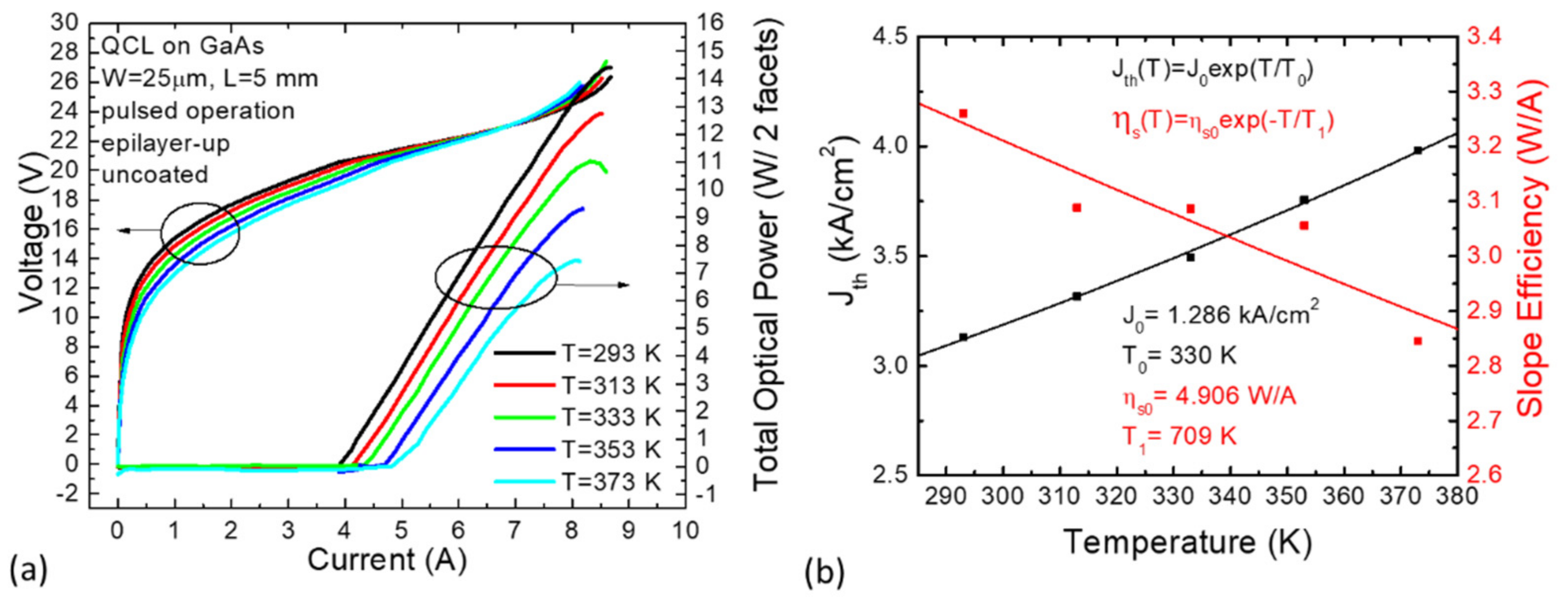
The temperature dependence of the laser performance was also measured, up to a temperature of 373 K (100 °C), as shown in
Figure 4a. The threshold and slope efficiency (η
s) trends were fit to exponential functions, giving characteristic temperatures of 330 K and 709 K, respectively [
11]. These numbers are comparatively higher than typical for this active layer design (T
0 = 285 K, T
1 = 459 K). However, part of this shift is due to the relatively high starting threshold and low slope efficiency at 293 K, which causes a correlated shift in the prefactors (J
0, η
s0) of the fitting functions. Nevertheless, the absence of increased temperature sensitivity suggests that the energy barriers built into the laser band structure for preventing thermal leakage are more or less intact.
4. Discussion
As mentioned above, the demonstrated mid-infrared QCL on GaAs represents a significant improvement in the state-of-the-art for heterogeneous integration of QCLs on mismatched substrates. However, we have identified some straightforward issues to address in the next set of experiments.
First, the operating voltage is currently about 50% higher for the QCL on GaAs than for similar lasers on InP. The most likely explanation for this is a significant series resistance at the metamorphic buffer/GaAs interface. The simple fabrication process for this experiment passes current directly through this interface. Though the measured carrier concentration seems satisfactory at the junction, the crystal structure is highly dislocated. A straightforward solution to this problem is to realize a laser with two top contacts and lateral current injection through the lower InP buffer layer. This architecture was previously developed by our group for THz lasers, and can be readily adapted for this purpose [
13].
The second main issue is a higher than normal waveguide loss, which may be due to scattering the presence of surface roughness in the waveguide core. Reduction in roughness is therefore expected to reduce waveguide loss as well. Follow-on work can explore ways to further reduce the surface roughness of the crystal surface during growth. A simple modification that is likely to have a strong effect is the use of a thicker InP buffer layer between the GaAs substrate and laser core. With a reduced voltage defect and a decrease in waveguide loss of 2–3 cm−1, the wallplug efficiency of the QCL on GaAs can be effectively doubled. This would create a real opportunity for high-power continuous wave operation as well.
5. Conclusions
In conclusion, a practical demonstration of a mid-infrared laser with high peak output power has been demonstrated by growing an InP-based QCL directly on a GaAs substrate. The device is demonstrated with only a simple InP buffer layer in between the substrate and the laser core. A 3 order of magnitude increase in output power has been realized compared to recent literature. With further development of a lateral current injection scheme and a thicker buffer layer, there is a very high probability of achieving similar performance to QCLs grown on InP substrate. This approach is directly adaptable for realization of QCLs on Si substrates as well.
Author Contributions
Conceptualization, M.R. and S.S.; investigation, S.S.; formal analysis, S.S.; writing—original draft preparation, S.S.; writing—review and editing, M.R.; project administration, M.R. All authors have read and agreed to the published version of the manuscript.
Funding
This research received no external funding.
Institutional Review Board Statement
Not applicable.
Informed Consent Statement
Not applicable.
Data Availability Statement
The data presented in this study are available on reasonable request from the corresponding author.
Conflicts of Interest
The authors declare no conflict of interest.
References
- Wang, F.; Slivken, S.; Wu, D.H.; Lu, Q.Y.; Razeghi, M. Continuous wave quantum cascade lasers with 5.6 W output power at room temperature and 41% wall-plug efficiency in cryogenic operation. AIP Adv. 2020, 10, 055120. [Google Scholar] [CrossRef]
- Zhou, W.; Wu, D.H.; McClintock, R.; Slivken, S.; Razeghi, M. High performance monolithic, broadly tunable mid-infrared quantum cascade lasers. Optica 2017, 4, 1228. [Google Scholar] [CrossRef]
- Lu, Q.; Wang, F.; Wu, D.; Slivken, S.; Razeghi, M. Room temperature terahertz semiconductor frequency comb. Nat. Commun. 2019, 10, 2403. [Google Scholar] [CrossRef] [PubMed]
- Abramov, P.I.; Kuznetsov, E.V.; Skvortsov, L.A. Prospects of using quantum-cascade lasers in optoelectronic countermeasure systems: Review. J. Opt. Technol. 2017, 84, 331. [Google Scholar] [CrossRef]
- Spitz, O.; Didier, P.; Durupt, L.; Díaz-Thomas, D.A.; Baranov, A.N.; Cerutti, L.; Grillot, F. Free-Space Communication with Directly Modulated Mid-Infrared Quantum Cascade Devices. IEEE J. Sel. Top. Quantum Electron. 2022, 28, 1200109. [Google Scholar] [CrossRef]
- Fuchs, F.; Hugger, S.; Jarvis, J.; Blattmann, V.; Kinzer, M.; Yang, Q.K.; Ostendorf, R.; Bronner, W.; Driad, R.; Aidam, R.; et al. Infrared hyperspectral standoff detection of explosives. Proc. SPIE 2013, 8710, 87100I. [Google Scholar] [CrossRef]
- Lin, H.; Luo, Z.L.; Gu, T.; Kimerling, L.C.; Wada, K.; Agarwal, A.; Hu, J. Mid-infrared integrated photonics on silicon: A perspective. Nanophotonics 2018, 7, 393. [Google Scholar] [CrossRef]
- Razeghi, M.; Defour, M.; Blondeau, R.; Omnes, F.; Maurel, P.; Acher, O.; Brillouet, F.; C-Fan, J.C.; Salerno, J. First cw operation of a Ga0.25In0.75As0.5P0.5—InP laser on a silicon substrate. Appl. Phys. Lett. 1988, 53, 2389. [Google Scholar] [CrossRef]
- Shi, B.; Han, Y.; Li, Q.; Lau, K.M. 1.55-μm Lasers Epitaxially Grown on Silicon. IEEE J. Sel. Top. Quantum Electron. 2019, 25, 1900711. [Google Scholar] [CrossRef]
- Go, R.; Krysiak, H.; Fetters, M.; Figueiredo, P.; Suttinger, M.; Leshin, J.; Fang, X.M.; Fastenau, J.M.; Lubyshev, D.; Liu, A.W.K.; et al. Room temperature operation of quantum cascade lasers monolithically integrated onto a lattice-mismatched substrate. Appl. Phys. Lett. 2018, 112, 031103. [Google Scholar] [CrossRef]
- Bai, Y.; Bandyopadhyay, N.; Tsao, S.; Slivken, S.; Razeghi, M. Room temperature quantum cascade lasers with 27% wall plug efficiency. Appl. Phys. Lett. 2011, 98, 181102. [Google Scholar] [CrossRef]
- Wang, F.; Slivken, S.; Wu, D.H.; Razeghi, M. Room temperature quantum cascade lasers with 22% wall plug efficiency in continuous-wave operation. Opt. Exp. 2020, 28, 17532. [Google Scholar] [CrossRef] [PubMed]
- Lu, Q.Y.; Wu, D.H.; Sengupta, S.; Slivken, S.; Razeghi, M. Room temperature continuous wave, monolithic tunable THz sources based on highly efficient mid-infrared quantum cascade lasers. Sci. Rep. 2016, 6, 23595. [Google Scholar] [CrossRef] [PubMed] [Green Version]
| Publisher’s Note: MDPI stays neutral with regard to jurisdictional claims in published maps and institutional affiliations. |
© 2022 by the authors. Licensee MDPI, Basel, Switzerland. This article is an open access article distributed under the terms and conditions of the Creative Commons Attribution (CC BY) license (https://creativecommons.org/licenses/by/4.0/).

