Communication

Degradation Characteristics and Mechanism of High Speed 850 nm Vertical-Cavity Surface-Emitting Laser during Accelerated Aging

1
State Key Laboratory of High Power Semiconductor Laser, Changchun University of Science and Technology, Changchun 130022, China
2
College of Physics & Electronic Information, Baicheng Normal University, Baicheng 137000, China
3
Science and Technology on Reliability Physics and Application of Electronic Component Laboratory, The Fifth Electronic Research Institute of the Ministry of Industry and Information Technology, Guangzhou 511370, China
*
Author to whom correspondence should be addressed.
Photonics 2022, 9(11), 801; https://doi.org/10.3390/photonics9110801
Submission received: 31 August 2022 / Revised: 19 October 2022 / Accepted: 21 October 2022 / Published: 26 October 2022
(This article belongs to the Special Issue Vertical-Cavity Surface-Emitting Lasers (VCSELs))

Abstract

:
The degradation process of Vertical-cavity Surface-emitting lasers with high speed and a central wavelength at 850 nm is investigated via constant-current accelerated aging experiments. Degradation of the photoelectric performances under different operating conditions are characterized by optical output power, and forward and reverse bias current–voltage. The 1/f noise characteristics and formation mechanism are discussed in terms of the experimental results of low frequency noise below threshold current. The main composition of low frequency noise before and after aging, the bias current dependence and the origin of the noise are analyzed emphatically. The correlation between the degradation suggests that the loss of photoelectric performance and the fluctuation of low frequency noise characteristic can be attributed to the contagion of defects towards the active region of Vertical-cavity Surface-emitting lasers. Furthermore, the results of failure analysis confirmed the conclusion that the contagion of defects occurred towards the active region of the samples after aging.

1. Introduction

At present, Vertical-cavity Surface-emitting laser (VCSEL) is in a period of rapid development as a very critical photo-source for high-speed optical network systems [1,2], owing to the advantageous properties of VCSEL technology, such as low cost, small size, circular beam shape, low divergence angle, low threshold current, high-speed modulation, on-wafer testing and ease of integration [3,4,5]. So far, VCSELs of various emission wavelengths have been extensively researched and some of them have even been gradually commercialized. In particular, 850 nm VCSELs are widely used in optical data communications at relatively short distances [6,7]. However, the degradation, or the failure, of devices in the optical communication system have caused a lot of severe problems which could result in the failure of the system, such as the noise of data, distortion and time-delay. Therefore, it is essential to the commercialization of VCSELs to improve their long-term stability. In the past two decades, investigators have carried out research on the reliability and failure mechanism of VCSELs. In 2003, Suning Xie et al. [8] investigated the reliability and failure mechanism of oxide VCSELs in high humidity and high temperature. Three failure modes of oxide VCSELs at biased 85/85 testing were identified, and the most common failure mode was dislocation growth. In 2009, Keun Ho Rhew et al. [9] investigated the long-term reliability of all monolithic 1.55-µm etched-mesa VCSELs with tunnel junction, via high-temperature storage tests and accelerated life tests. The failure mechanism was analyzed based on degradation modes. In 2013, Robert W. Herrick et al. [10] demonstrated the corrosion failure mechanism of oxide aperture VCSELs. Cracks near the tip of the oxide aperture caused line dislocations, which, in turn, caused the growth of climb dislocations (DLDs) in the active region. In 2019, A. W. Bushmaker et al. [4] presented a hypothesis attributing the location of the defects around the oxide aperture edge to current crowding in that area, which increased electrical and thermal stress in this region. The fluctuation of photoelectric characteristic parameters in the aging process was the most intuitive manifestation of their degradation. In the aging process, the degradation of photoelectric properties is studied, with the presence of defects and dislocations as the target, so as to build understanding of the degradation mechanisms that impede reliability of the devices and because it is helpful in further analyzing the epitaxial wafer quality of VCSELs.
In recent years, researchers have found that the 1/f noise is closely related to the lifetime of the semiconductor devices [11,12,13]. Therefore, the analysis of the 1/f noise characteristic is used in the reliability evaluation of semiconductor devices, which is an effective method of non-destructive evaluation. Low-frequency noise is one of the most sensitive indicators of degradation of semiconductor lasers [14,15]. Specifically, internal defects, surface leakage and bad ohmic contact of the semiconductor laser increase low-frequency noise, and, therefore, the noise can be used to reflect the microscopic degradation of the semiconductor laser after stress. In 1994, Fukuda, M. et al. [16] experimentally and theoretically investigated the origin of the l/f noise in BH semiconductor lasers under device degradation. The nonradiative recombination current increased during device degradation, then the l/f noise increased. In 2002, S. Pralgauskaite et al. [17] presented a method to evaluate laser diode reliability based on the measurement of low-frequency optical and electrical noise. The results indicated that the correlation factor changed during short-time aging. In 2010, ZL Li et al. [18] studied noise spectra of green GaN LEDs with three different indium doping concentrations to confirm the theory of enhanced defect densities increasing indium concentration. In 2022, Wenyuan Liao et al. [19] investigated properties of low-frequency noise of the commercially available VCSEL at 1310 nm wavelength. The results indicated that current noise power spectral density increased after the device aged, and the noise increased with the augmentation of electrical stress. However, there have rarely been any reports investigating the degradation mechanism of 850 nm VCSELs during accelerated aging, based on low-frequency noise at home and abroad.
In this paper, the degradation characteristics and mechanism of high speed 850 nm VCSELs are investigated during accelerated aging. Photoelectric characteristics and low-frequency noise characteristics are used to analyze the degradation mechanism of the devices under high current stress accelerated aging tests. According to the results of the 1/f noise tests, the origin of the 1/f noise was analyzed. When the bias current was lower than the threshold current, the noise of VCSELs mainly originated from the active region. The conclusion that the contagion of defects towards the active region of the samples after aging was confirmed by the failure analysis.

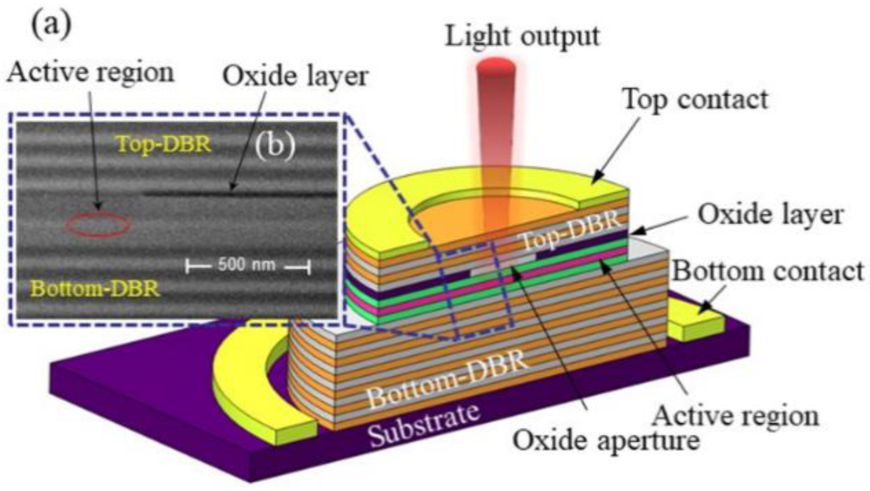
2. Device Structure and Experimental Details

The schematic diagram of the VCSELs, discussed in the following section of performance characterization, is shown in Figure 1a. The epitaxial structural layers of the VCSEL were grown by metal-organic chemical vapor deposition (MOCVD). The layers were grown on an n-type GaAs substrate. The λ-cavity was made up of 240 nm Al0.3Ga0.7As spacer. In the middle, the active region was composed of three 10 nm GaAs quantum-well layers with 8 nm Al0.3Ga0.7As barriers in between the wells. Eighteen pairs of p-type doped Distributed Bragg Reflectors (DBRs) were above the λ-cavity, and 40.5 pairs n-type doped DBRs below the λ-cavity. Each pair of DBRs were composed of AlGaAs layers with high and low aluminum component number. Figure 1b shows the FIB-SEM image in cross section of the active region of the VCSEL. The chips were packaged using TO- 46 headers with cover glass. At room-temperature, the typical peak wavelength of the studied VCSEL was at 850 nm.
In order to obtain accurate and reliable test results, all packaged devices that were used in this test came from the same wafer, and the selected devices were tested before aging to avoid unstable performance or fast failure in the early stage of the test. The devices were installed on the fixture of the aging system, and the built-in current source of the system generated constant currents.
The electrical aging test was carried out under forward constant current stress of 12 mA, 15 mA, 17 mA and 20 mA, respectively. The electrical and optical characteristics were monitored, and the temperature in the course of aging was set at 35 °C. To clearly gauge the device degradation caused by current stress, the test on electrical and optical characteristics of the devices after aging were carried out at room temperature. Three VCSELs with identical characteristics were used in each set of experiments. The parameters of the VCSELs were monitored for optical output power, current–voltage characteristic and low-frequency noise at the preaging and the intermediate stages.
The electrical and optical characteristics were measured by a semiconductor device analyzer (Model: Agilent B1500A) and a photoelectric detector (Model: PM-100D). Low-frequency noise measurements were measured by using a dynamic signal analyzer (Model: SR785), while a filter and amplifier units were provided by Proplus 9812B. Low-frequency noise measurements (1 Hz–1 kHz) were measured before aging, after 624 h aging and after 1000 h aging, respectively. Electroluminescence characterizations were carried out by photo emission microscope (PEM) (Model: PHEMOS-1000). The micro-structures were analyzed by means of a scanning electron microscope (FIB-SEM) DualBeam System (Model: Helios G4 CX), and transmission electron microscopy (TEM) (Model: Tecnai G2 F20 S-TWIN).

3. Results and Discussion

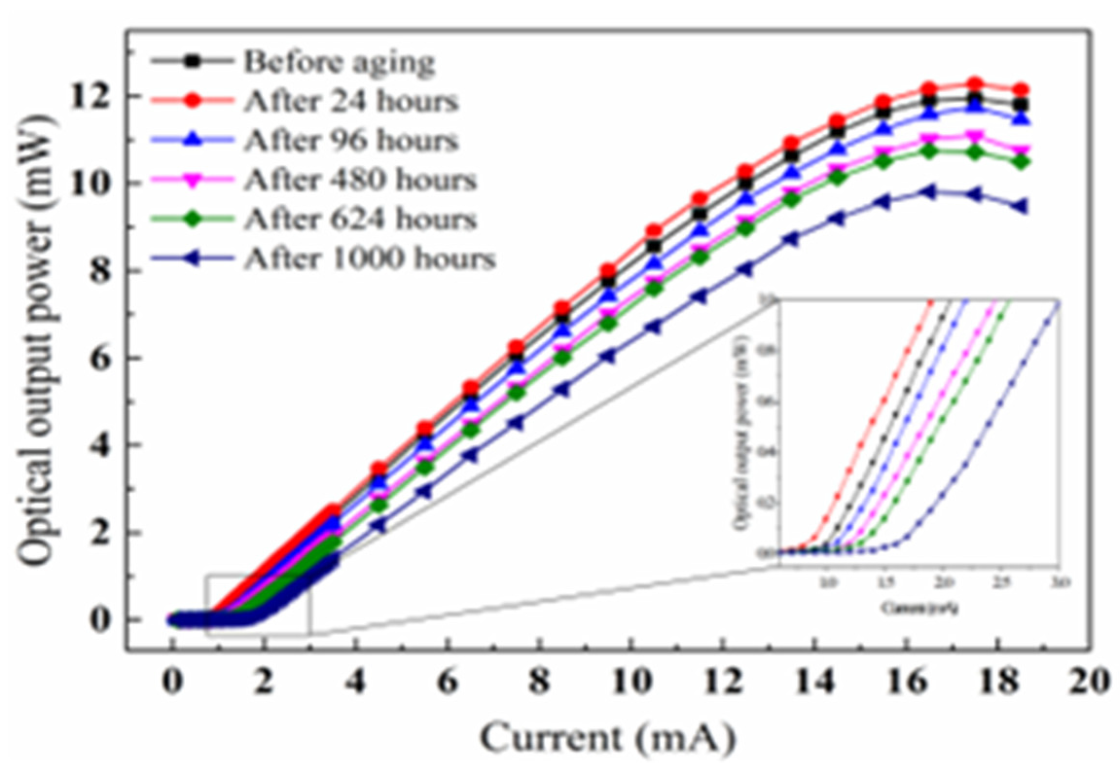
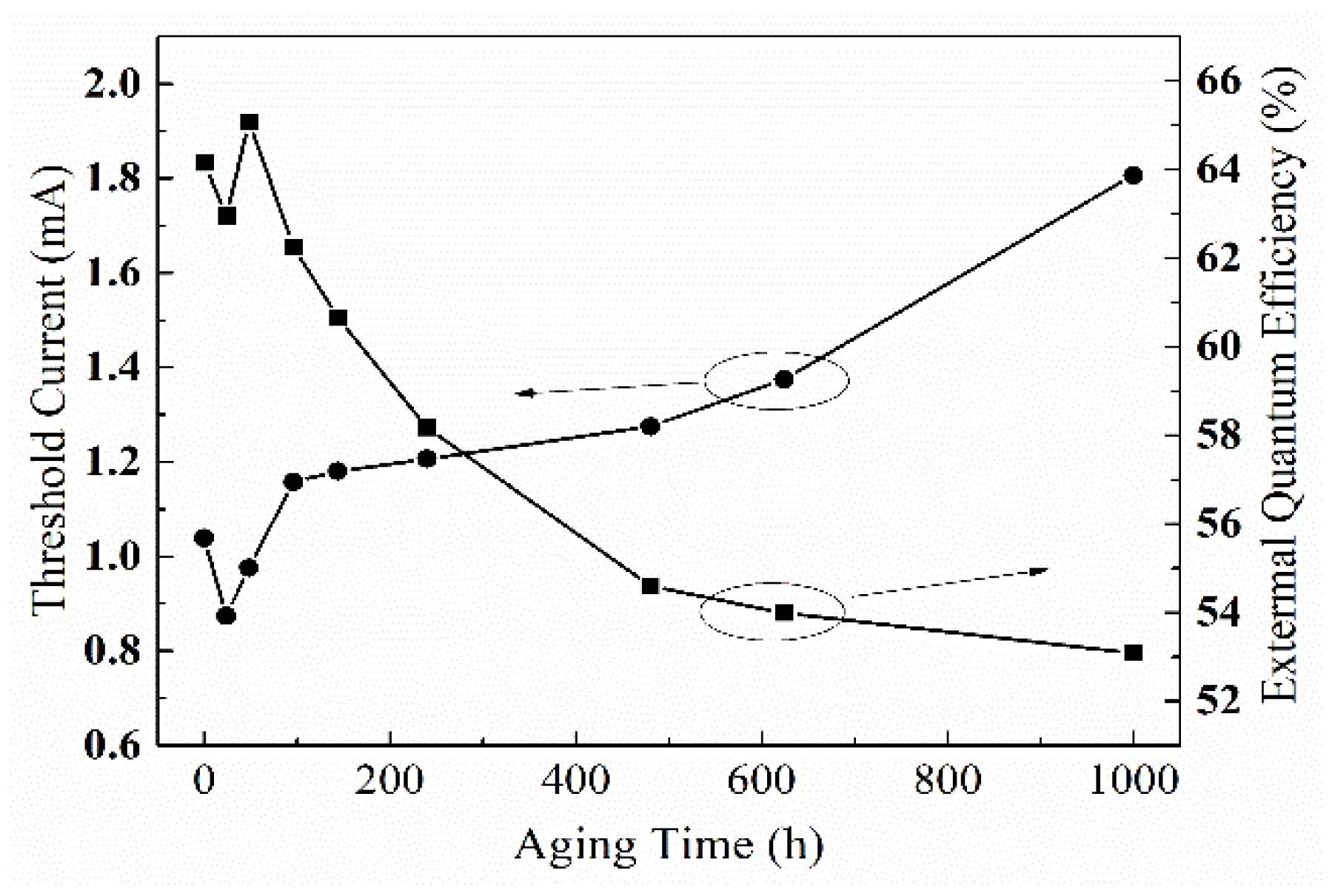
3.1. Effect of Accelerated Aging on Optical Output Characteristics

The characteristic variations of the optical output power with bias current during the accelerated aging are presented in Figure 2. The electrical aging stress was set at 20 mA. The power saturation currents were basically unchanged, and the error for all measured values was less than 0.01 mW. It was observed that the threshold current and the output optical power present clearly changed. Threshold current and external quantum efficiency, versus aging time curves, were plotted in Figure 3. In the early stage of aging, the threshold current decreased from 1.04 mA to 0.87 mA, and the output optical power increased by 2.8%. This phenomenon was caused by the annealing effect. The annealing effect refers to the photoelectric performance of the device which is recovered when positive bias is carried out. It can be explained by the compound enhanced defect [20]. The rate of defect recombination is linearly correlated with the density of the charge injection. As the number of defects decreases, the threshold current is gradually recovered. At the same time as the nonradiative recombination decreases, the junction temperature of the device decreases, the number of photons produced by carrier recombination increase, and the output optical power increases. Whereas, after 96 h aging, the threshold current increased, as shown in the inset of Figure 2, the output optical power and the external quantum efficiency decreased. This indicated that the degradation of the VCSELs was gradually activated.
The slope efficiency is defined as the slope of the linear part on the optical output power versus current curve of the VCSEL with laser mode, which represents the ability of the VCSEL to transform current-carriers into photons. The external quantum efficiency (EQE) can be expressed by the slope efficiency ηd, as follows [21]:
η e = η d e λ h c
where ηe is the EQE, ηd is the slope efficiency, λ is the operating wavelength, h is Planck’s constant, c is speed of light. EQE can more intuitively reflect the degradation of the quantum well region with aging conditions. The calculation results of EQE with aging time are shown in Figure 3. EQE gradually decreased with the increase of aging time. After 1000 h aging, EQE had degenerated to 82.76% compared with that before aging. As defects proliferated after aging, the nonradiative recombination center increased and recombined some carriers, and the number of photons generated per second decreased when the number of electron hole pairs injected into the active region were constant per unit time. Therefore, EQE decreased with increased aging time.

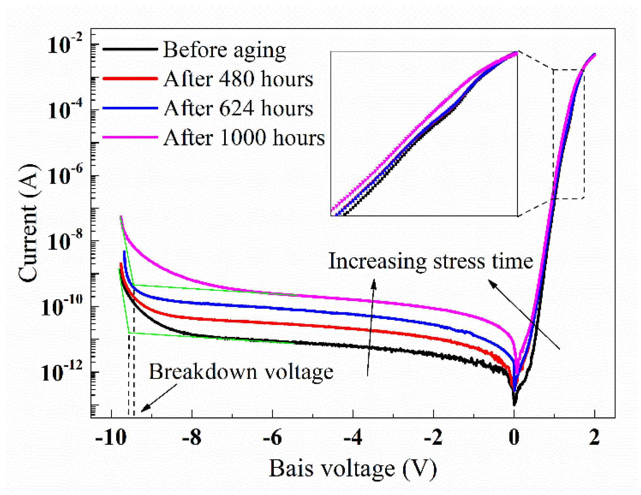
3.2. Effect of Accelerated Aging on the Forward and Reverse Current–Voltage

The forward and reverse current–voltage characteristics of devices before and after aging is shown in Figure 4. The electrical aging stress was set at 20 mA. When the forward bias voltage was lower than 1.5 V, the forward current increased obviously with aging time. The carrier injection into the active region was mainly by means of the tunneling mechanism [14,22], which was mainly through the defect located in the space charge region, and was dominated by nonradiative recombination. When the forward voltage was in the 1.5 V to 2 V range, as shown in the inset of Figure 4, the forward current increased slightly with the aging time. The injected carriers diffused through the whole active region, which was dominated by radiation recombination. When the forward bias voltage was larger than 2 V, the forward current did not obviously change with aging time. In this case, the influence of series resistances (from bulk resistances and contact resistances) could not be ignored, and the compound current dominated at this time.
An early indication of device degradation could be obtained by monitoring reverse leakage current. We observed that the leakage current increased and reverse bias breakdown voltage decreased after the accelerated aging. Compared with preaging, the leakage current after 1000 h aging increased by nearly two orders of magnitude. The phenomenon can be illustrated by the tunneling mechanism. The long-term constant current aging stress increases the temperature of the active region, and the carriers from thermal excitation at high temperature cause an increase of the tunneling dislocations. It is easy for the carriers to escape the restriction of the quantum barrier, resulting in an increase in the leakage current.
The leakage current was observed under both reverse bias and forward bias, indicating that the tunneling current increased. The nonradiative recombination rate increased with the increase of defects in the active region, resulting in additional tunneling current. The leakage current increased when aging time increased, which corresponded to the continuous attenuation of the optical power and the increase of threshold current.

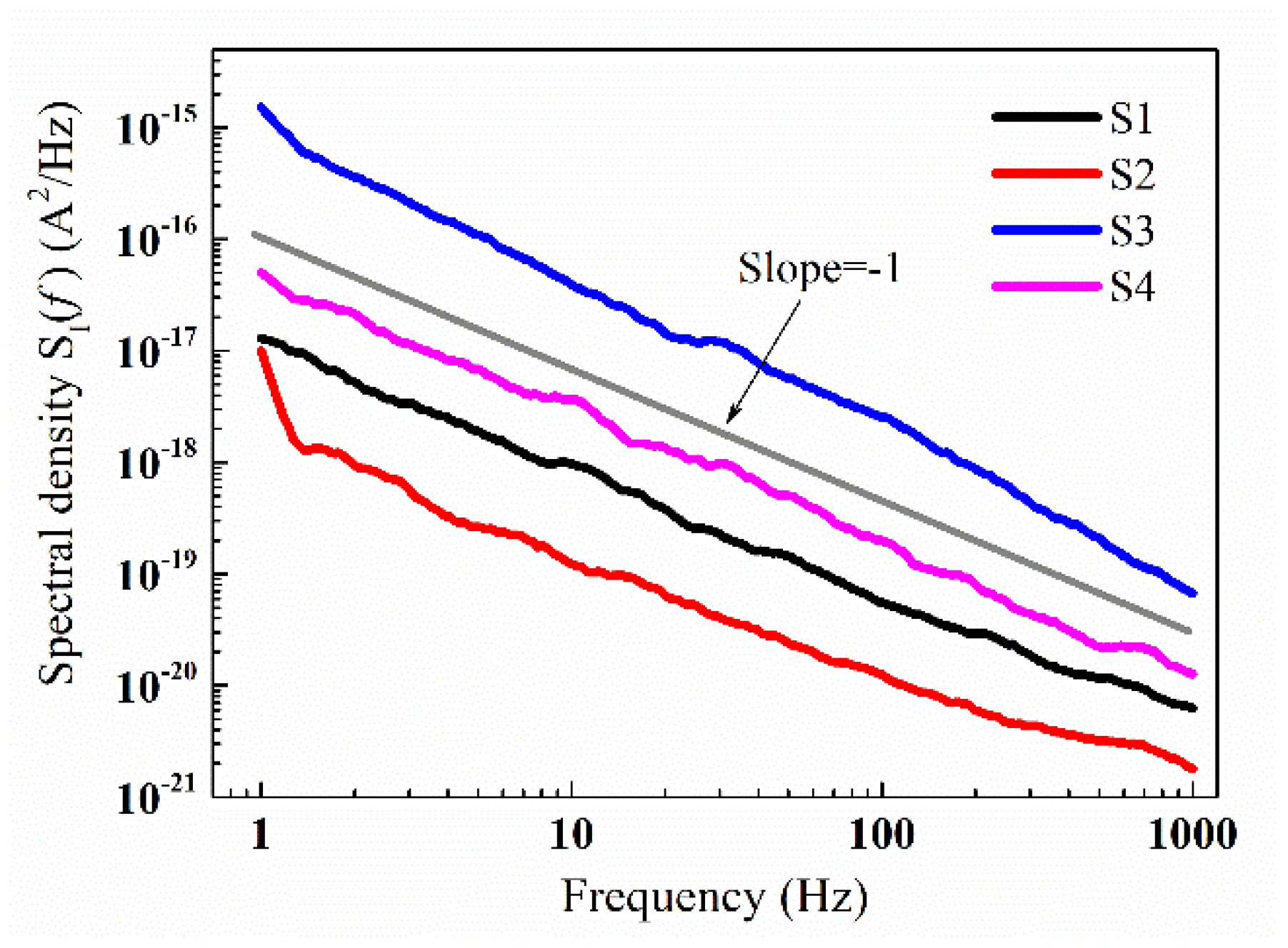
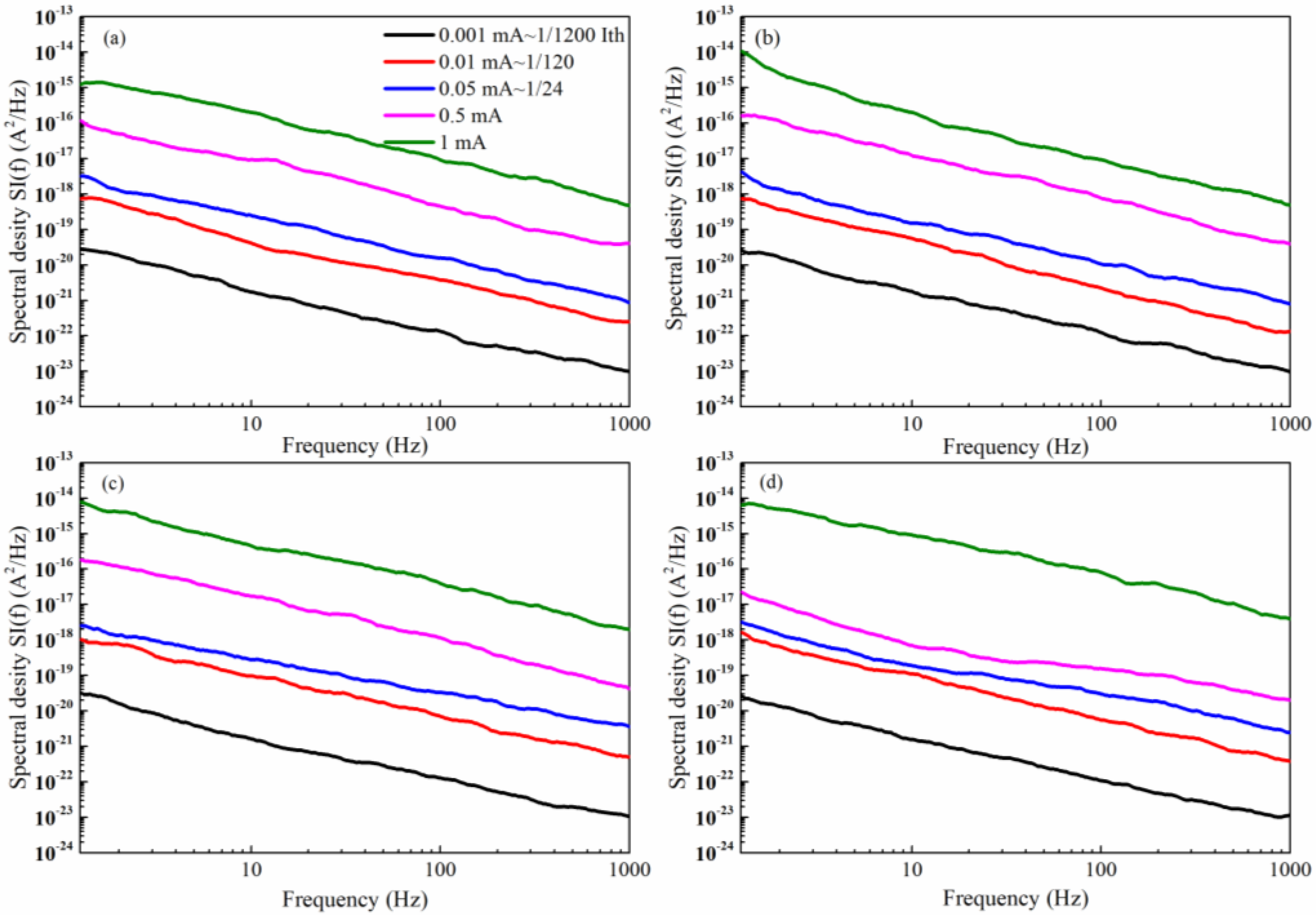
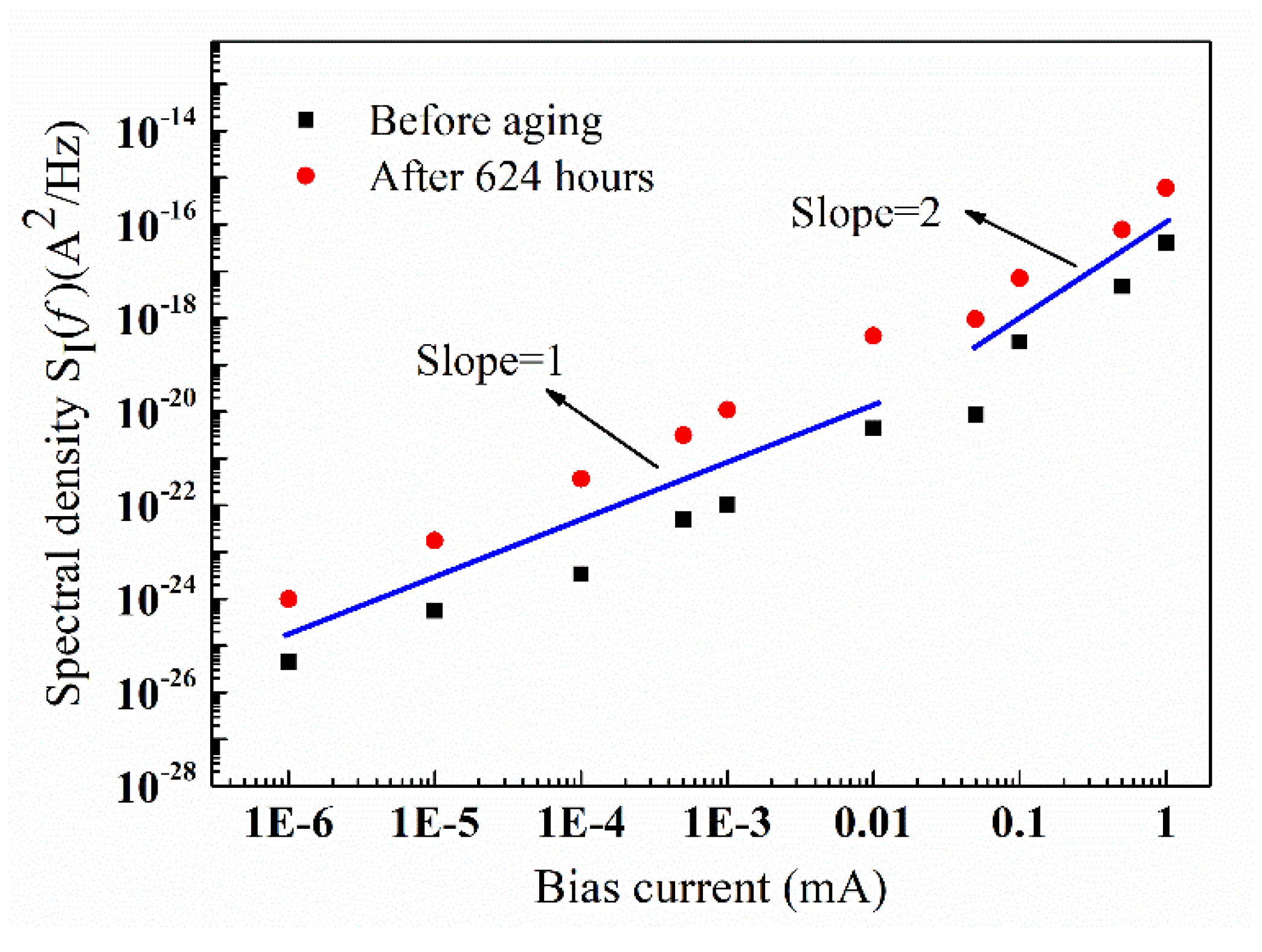
3.3. Effect of Accelerated Aging on Low-Frequency Noise

The 1/f noise is dominant in the low-frequency noise produced by the PN junction semiconductor laser, and, thus, investigation of 1/f noise characteristics is more valuable for the semiconductor laser than other low-frequency noise. To analyze the origin of the 1/f noise, a simplified equivalent circuit was used, shown in Figure 5 (the case of the parallel leakage of laser diode was considered). When bias current was lower than the threshold current, the electrical characteristic of the laser diodes could be approximately modeled as that of typical diodes, mainly composed of the PN junction dynamic resistance Rd, the contact resistance Rc and the leakage resistance Rp [23].
According to the simplified equivalent circuit and the Hooge equation [24], the 1/f noise power spectral density of semiconductor lasers can be described as follows:
S V f = 2 3 α m k T 2 q I S f τ n + α N c f R C 2 I S 2 + α N p f R P 2 I P 2
where, α is the Hooge constant, m is the extrinsic factor, k is the Boltzmann constant, Rc is the contact resistance, Rp is the leakage resistance, Is is the reverse saturation current, Ip is the leakage current, q is the electron charge, T is the absolute temperature, Nc is the total carrier density in the contact resistance, and Np is the total carrier density in the leakage resistance. Therefore, at low bias current range, the major noise of laser diodes was generated from the active region dynamic resistance, the contact resistance and the leakage resistance.
At low bias, low-frequency noise is susceptible to the degradation of the active region of the semiconductor laser [23]. When the investigation of the semiconductor laser is limited below threshold current for operation, photons are generated by electron-hole combination in the junction region of the semiconductor laser, which is in a spontaneous emission state. The electrical behavior of the semiconductor laser is determined by the properties of the hetero-junction in this state. Therefore, the influence of the 1/f noise from the stimulated emission was ignored.
The current noise power spectral density curves of the typical samples with bias current 0.1 mA are shown in Figure 6. Compared with the reference curve (the slope was −1), the current noise power spectral density curves were nearly parallel, which indicated that the noise component in this frequency band was mainly composed of the 1/f noise. The 1/f noise characteristics were tested for 12 preaging samples. All the results showed the 1/f noise features, but there were differences in the noise intensities.
In order to analyze the dependence of low-frequency noise on electrical aging stress, the typical results were selected for demonstration. The current noise power spectral density versus frequency at different bias currents are shown in Figure 7a–d. The electrical aging stresses were set as 12 mA, 15 mA, 17 mA and 20 mA, respectively. The results of the 1/f noise characteristics of the samples were measured after 1000 h aging. In the operating conditions for the low bias current (below the threshold current) and low frequency band (1 Hz~1 kHz), the current power spectral density of the 1/f noise samples was analyzed. The different samples presented similar regularity in the same aging condition and bias current, and the distinctions were mainly reflected in the noise intensities. The experimental results showed that the current noise power spectral density of all the tested samples decreased with frequency increasing, and current noise power spectral density increased with the bias current in the low frequency band. Compared with the power spectral density of the 1/f noise samples before aging, all the spectral densities of the 1/f noise of devices in this frequency range increased.
Meanwhile, the characteristic parameters of the 1/f noise were also studied. Current noise power spectral density curves in Figure 7 were fit at different bias current to obtain the frequency exponential factor γ and the amplitude of the 1/f noise at f = 1 Hz, as shown in Table 1. The results showed that the amplitude of the 1/f noise gradually increased with the increment of the bias current. The fluctuation of frequency exponential factor γ was around 1. These results showed that the noise component in the frequency range was mainly composed of 1/f noise.
In order to analyze the dependence of low-frequency noise on aging time, a typical result was selected for demonstration. The measured low-frequency noise behaviors of the samples in the aging process are shown in graphs in Figure 8 and Figure 9. From Figure 8, we can see that the noise power spectral density after 1000 h aging was nearly two orders of magnitude higher than that before aging when the bias current was 0.1 mA. In addition, it can also be seen from Figure 9 that the noise level of the sample after aging was larger than the sample before aging, which indicated that there were more internal defects created in the active region during the aging process. The case was closely related to the reliability of VCSELs.
Figure 9 shows the current noise power spectral density (both before and after aging) as a function of the bias current for the samples, where SI represented the noise power spectral density values at 20 Hz. The results showed that the variation of the current noise power spectral density intensities was closely related to the bias current, and the variation trend was almost identical before aging and after aging. The current noise power spectral density increased after aging. The result indicated that the active region defects of the device increased with the increase of aging time, and the performance degraded more seriously. Clearly, below the threshold current, the effects of bias current on VCSELs were dominant, and constant-current stress accelerated aging had an obvious influence on the 1/f noise fluctuation of the VCSEL.
The active region of VCSELs contain a multiple quantum-wells structure. In this region of the VCSEL, the current is continuously injected. Diffusion and carrier recombination act to determine the fluctuation of current noise. The injected carriers are transferred to the multiple quantum-well region through the diffusion process. The carriers are delivered to the multiple quantum-wells by tunneling through the barriers and they are restricted in the multiple quantum-wells region. At the condition of the low bias current injection, the conducting current is determined by the process of the diffusion, the rate of the spontaneous inter-band recombination in the quantum-wells, the rate of nonradiative recombination from defect levels located at the interface and bulk of the laser diodes, and the rate of carrier tunneling through the barriers between the quantum-wells [14]. The diffusion process produced a diffusion of the 1/f noise linearly related to the bias current.
The location of the noise source could be revealed by the bias dependence of the 1/f noise. As can be seen in Figure 9, the current dependence of the 1/f noise was different in different ranges of bias current, indicating that different sources dominated the spectra of the 1/f noise in different bias ranges. In the bias current range between 1 nA and 10 μA, the curves show that the current noise power spectral density was linearly correlated with the bias current and a slope≈1 in the logarithm coordinate. From the first term in Equation (2), we know that the 1/f noise from the active region was linear in proportion to the bias current. Therefore, the 1/f noise in the range between 1 nA and 10 μA was from the active region. Moreover, it could also be observed that the curves changed slowly between 10 μA and 50 μA. Considering the first and third terms in Equation (2), the 1/f noise caused by series resistance was relatively weak, so it was ignored. The noise caused by the PN junction dynamic resistance decreased with the increase of current in series resistance, and the noise caused by leakage resistance increased with the increase of leakage current. The total noise curves show a transition region that did not change clearly with the increase of bias current. The reason was that more and more carriers were poured into the active region with the bias current increasing, and this caused increase in the recombination of the carriers and traps in the active region. At the same time, the carrier concentration in the series resistor reduced; hence, the current diffusion into the active region was restrained [25]. The two aspects above resulted in the 1/f noise intensity experiencing little change with the bias current. In the bias current range between 50μA and 1mA, the curves show linear correlation and a slope ≈ 2 in the logarithm coordinate, so the voltage drop across the series resistor could not be neglected. Therefore, the 1/f noise from the series resistor significantly increased with bias current I2 of the second term in Equation (2). Although we could see an increase in the magnitude, the I2 dependence of the current noise power spectral density was not affected by the stress. The drop in stress voltage mainly occurred the active region, which created defects in the active region. In conclusion, the noise of VCSELs below the threshold current mainly stems from the active region.

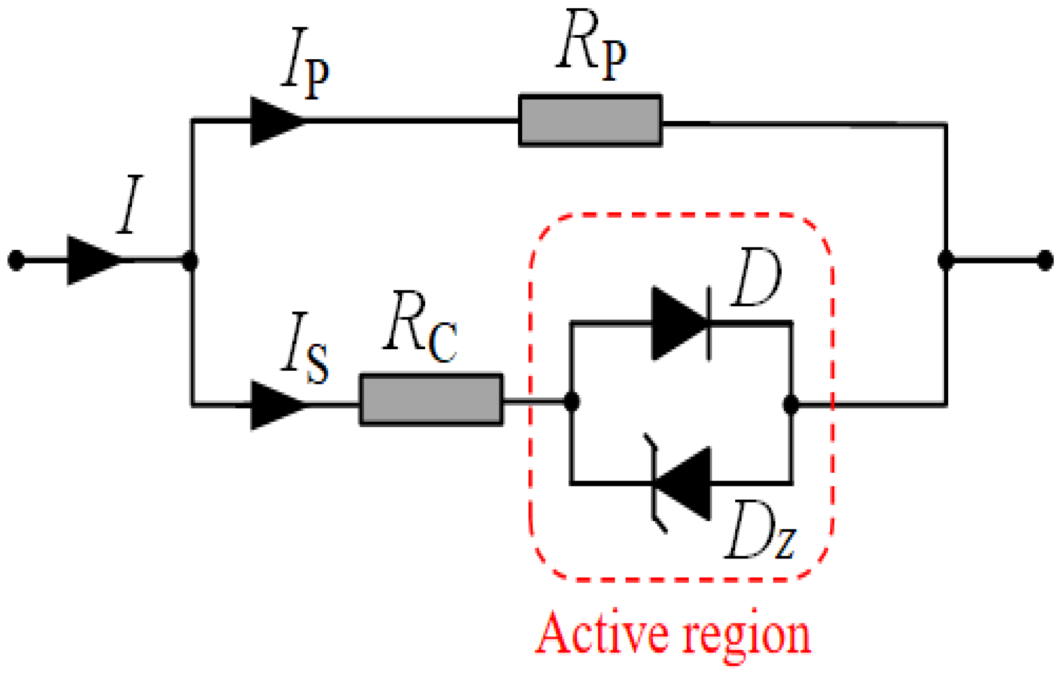
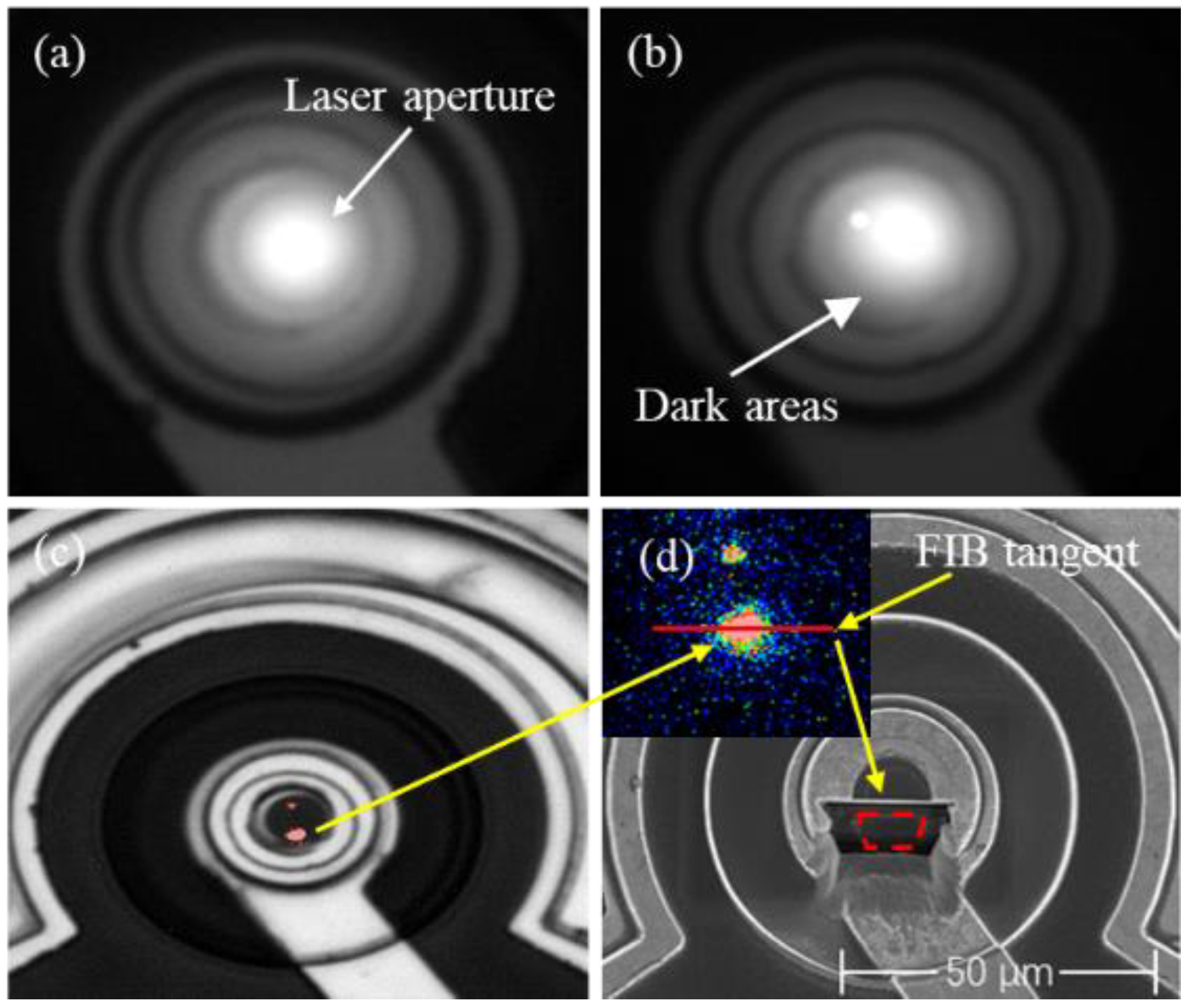
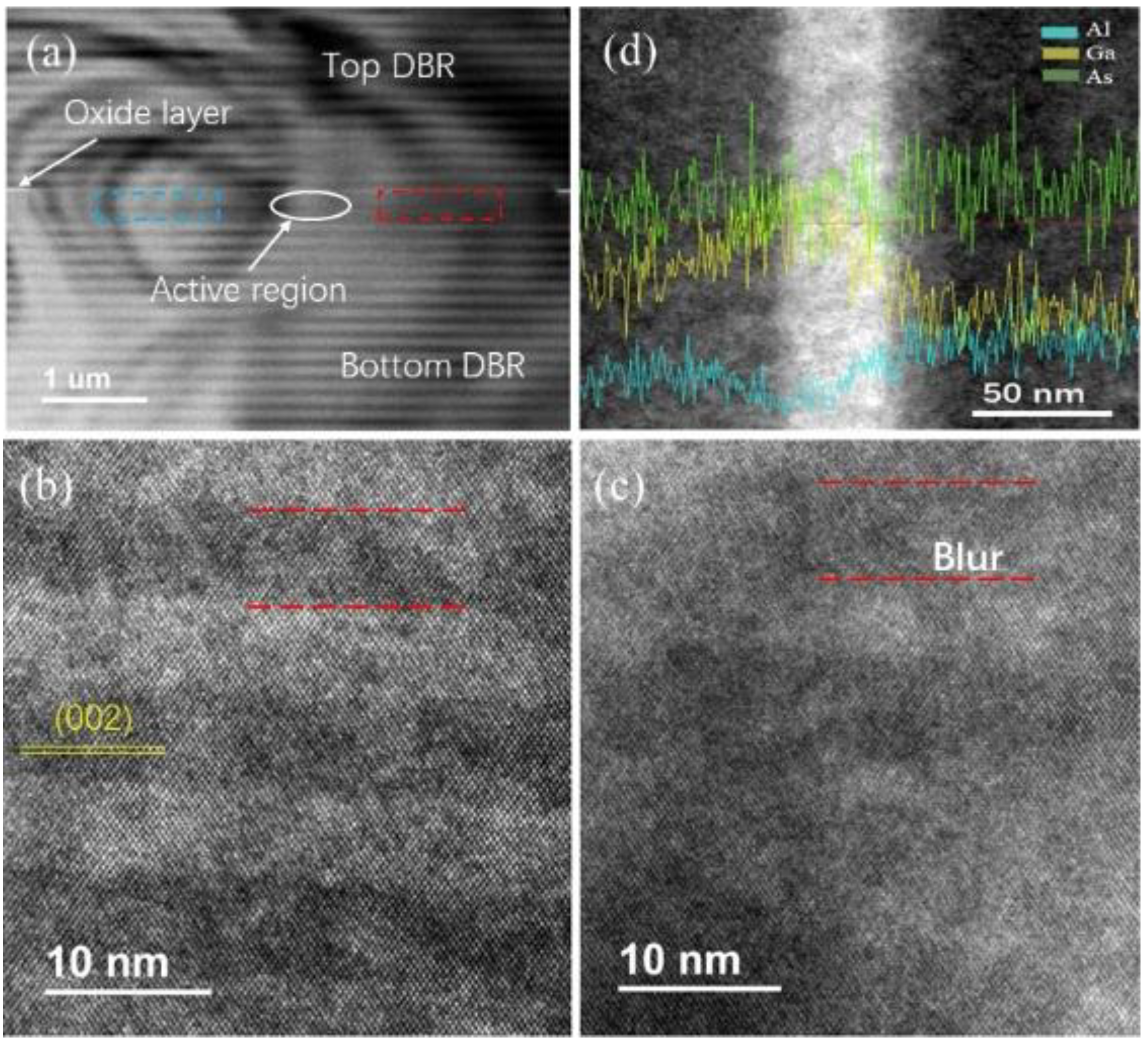
3.4. Effect of Accelerated Aging on Contagion of Defects

To confirm the evidence that the contagion of defects occurred towards the active region of the samples, failure analysis was carried out on the samples before and after aging.
When the forward bias voltages of the samples before and after aging were 1.3 V and 1.39 V, the electroluminescence images are shown in Figure 10a,b. The emission intensity of the sample after aging was obviously lower than that before aging, and the distribution of the emission intensity of the sample was obviously uneven, and the emission dark area appeared. The total optical power and emission efficiency decreased, which was consistent with the attenuation of the optical output power of the sample after aging. When a reverse bias voltage of 9.16 V was carried out to the sample after aging, the EMMI image located the defect of the sample, as shown in Figure 10c. There were two abnormal light spots (red area) on the edge of the light output aperture. It could be judged that the defects proliferation was located in the red areas, as there was the path of current in the areas, leading to the increase of forward current and reverse leakage current. In order to reveal the microstructure changes in the dark area of the sample after aging, a dual-beam system focused ion beam was used to cut and mill the dark area, as shown in Figure 10d. The colorized close-up of the insert of Figure 10d corresponded to the red dots region in Figure 10c, and the solid line showed the position of FIB in Figure 10d.
The TEM image of the FIB cross section is shown in Figure 11a. The TEM image revealed that some areas in the quantum well hetero-junction of the active region of the sample after aging were blurred. The defects seemingly originated from the active layers under the oxide layer. Figure 11b,c show a magnified image of the region of interest (the bule box and the red box) in Figure 11a. Figure 11b shows that the hetero-junction interface was flat, without obvious structural fluctuation. Grain boundaries were clear and no obvious defects were observed. Figure 11c shows that the hetero-junction interface appeared blurred, and a large number of high-density dislocation defects were generated, which spread to the surrounding areas. Usually, the electrically accelerated aging, or ESD damage, dislocation defects generate in the active region of VCSEL [26,27], which leads to the contagion of dislocation defects, and these dislocation defects sprawl to the surrounding area under electrical stress. Further, an EDS-line scan was used to analysis the element distribution of the sample, as shown in Figure 11d. The distribution curves of Ga and Al elements fluctuated near the hetero-junction interface, and the diffusion phenomenon of Ga and Al elements appeared, which became point defects. When the point defects accumulate to a certain extent to form dislocations, they eventually lead to failure.

4. Conclusions

In this work, the optical and electrical characteristics of VCSELs were studied under constant-current stress aging. In the early stage of aging, the annealing effect appeared in the devices. After 96 h aging, the optical output power and EQE decreased with the increase in aging time. An increase of tunneling current was observed under both forward bias and reverse bias. Reverse bias breakdown voltage decreased after aging, indicating that the VCSELs degraded gradually in the active region. Further, the results of low-frequency noise indicated that the noise component of all the tested devices before and after aging mainly consisted of the 1/f noise. With increase of aging time, the active region defects of the device increased, and the performance degradation became more serious. When the bias current was lower than the threshold current, the effects of bias current on the 1/f noise of VCSELs were dominant, and the noise mainly stemmed from the active region. The results of defect localization and micro-structure analysis of the samples after aging confirmed the evidence that ‘contagion of defects towards the active region of VCSELs’ were the reason for the ‘degradation in photoelectric performance and fluctuation of low frequency noise characteristic’.
The degradation of the VCSEL during the aging process was non-destructively monitored in our tests. Under a small bias current, the 1/f noise of VCSELs was created in the active region and the contact resistance could be measured. Consequently, the method could be used to non-destructively monitor the degradation law and evaluate the reliability of VCSELs. In short, the research is helpful in quality inspection and reliability evaluation of VCSELs.

Author Contributions

Conceptualization, investigation, writing-original draft preparation, J.Z.; formal analysis, validation, writing-review and editing, W.L.; supervision, X.W. and G.L.; project administration, S.Y.; methodology, Z.W. All authors have read and agreed to the published version of the manuscript.

Funding

This work was funded by the Open-Foundation of Key Laboratory of Laser Device Technology, China North Industries Group Corporation Limited, grant No KLLDT202105, and the Fundamentals and Application fundamentals of Guangzhou, grant No. 202201011150.

Institutional Review Board Statement

Not applicable.

Informed Consent Statement

Not applicable.

Data Availability Statement

Not applicable.

Conflicts of Interest

The authors declare no conflict of interest.

References

  1. Liu, A.; Wolf, P.; Lott, J.A.; Bimberg, D. Vertical-cavity surface-emitting lasers for data communication and sensing. Photonics Res. 2019, 7, 121–136. [Google Scholar] [CrossRef]
  2. Larisch, G.; Tian, S.; Bimberg, D. Optimization of VCSEL photon lifetime for minimum energy consumption at varying bit rates. Opt. Express 2020, 28, 18931–18937. [Google Scholar] [CrossRef] [PubMed]
  3. Healy, S.B.; O’Reilly, E.P.; Gustavsson, J.S.; Westbergh, P.; Haglund, Å.; Larsson, A.; Joel, A. Active Region Design for High-Speed 850-nm VCSELs. IEEE J. Quantum Electron. 2010, 46, 506–512. [Google Scholar] [CrossRef]
  4. Bushmaker, A.W.; Lingley, Z.; Brodie, M.; Foran, B.; Sin, Y. Optical Beam Induced Current and Time Resolved Electro-Luminescence in Vertical Cavity Surface Emitting Lasers During Accelerated Aging. IEEE Photonics J. 2019, 11, 1504011. [Google Scholar] [CrossRef]
  5. Koyama, F. Recent Advances of VCSEL Photonics. J. Light. Technol. 2006, 24, 4502–4513. [Google Scholar] [CrossRef]
  6. Kuchta, D.; Rylyakov, A.; Doany, F.; Schow, C.; Proesel, J.; Baks, C.; Westbergh, P.; Gustavsson, J.; Larsson, A. A 71-Gb/s NRZ modulated 850-nm VCSEL-based optical link. IEEE Photonics Technol. Lett. 2015, 27, 577–580. [Google Scholar] [CrossRef]
  7. Westbergh, P.; Safaisini, R.; Haglund, E.; Kögel, B.; Gustavsson, J.S.; Larsson, A.; Geen, M.; Lawrence, R.; Joel, A. High-speed 850 nm VCSELs with 28 GHz modulation bandwidth operating error-free up to 44 Gbit/s. Electron. Lett. 2012, 48, 1145–1147. [Google Scholar] [CrossRef] [Green Version]
  8. Xie, S.; Herrick, R.W.; Chamberlin, D.; Rosner, S.J.; McHugo, S.; Girolami, G.; Mayonte, M.; Kim, S.; Widjaja, W. Failure Mode Analysis of Oxide VCSELs in High Humidity and High Temperature. J. Light. Technol. 2003, 21, 1013. [Google Scholar]
  9. Rhew, K.H.; Jeon, S.C.; Lee, D.H.; Yoo, B.-S.; Yun, I. Reliability assessment of 1.55-μm vertical cavity surface emitting lasers with tunnel junction using high-temperature aging tests. Microelectron. Reliab. 2009, 49, 42–50. [Google Scholar] [CrossRef]
  10. Herrick, R.W.; Dafinca, A.; Farthouat, P.; Grillo, A.A.; McMahon, S.J.; Weidberg, A.R. Corrosion-Based Failure of Oxide-Aperture VCSELs. IEEE J. Quantum Elect. 2013, 49, 1045–1052. [Google Scholar] [CrossRef]
  11. Hasse, L.Z.; Babicz, S.; Kaczmarek, L.; Smulko, J.M.; Sedlakova, V. Quality assessment of ZnO-based varistors by 1/f noise. Microelectron. Reliab. 2014, 54, 192–199. [Google Scholar] [CrossRef]
  12. Del Vecchio, P.; Curutchet, A.; Deshayes, Y.; Bettiati, M.; Laruelle, F.; Labat, N.; Béchou, L. Correlation between forward-reverse low-frequency noise and atypical I–V signatures in 980 nm high-power laser diodes. Microelectron. Reliab. 2015, 55, 1741–1745. [Google Scholar] [CrossRef]
  13. Pralgauskaitė, S.; Palenskis, V.; Matukas, J.; Glemža, J.; Muliuk, G.; Šaulys, B.; Trinkūnas, A. Reliability investigation of light-emitting diodes via low frequency noise characteristics. Microelectron. Reliab. 2015, 55, 52–61. [Google Scholar] [CrossRef]
  14. Chen, X.Y.; Pedersen, A.; van Rheenen, A.D. Effect of electrical and thermal stress on low-frequency noise characteristics of laser diodes. Microelectron. Reliab. 2001, 41, 105–110. [Google Scholar] [CrossRef]
  15. Grüneis, F. An alternative form of Hooge’s relation for 1/f noise in semiconductor materials. Phys. Lett. A 2019, 383, 1401–1409. [Google Scholar] [CrossRef]
  16. Fukuda, M.; Hirono, T.; Kurosaki, T.; Kano, F. Correlation between 1/f noise and semiconductor laser degradation. Qual. Reliab. Eng. Int. 1994, 10, 351–353. [Google Scholar] [CrossRef]
  17. Pralgauskaite, S.; Matukas, J.; Palenskis, V.; Sermuksnis, E.; Vysniauskas, J.; Letal, G.; Mallard, R.; Smetona, S. Reliability and low-frequency noise measurements of InGaAsP MQW buried-heterostructure lasers. In Proceedings of the 14th International Conference on Microwaves, Radar and Wireless Communications. MIKON-2002. Conference Proceedings (IEEE Cat.No.02EX562), Gdansk, Poland, 20–22 May 2002; Volume 582, pp. 588–591. [Google Scholar]
  18. Li, Z.L.; Lai, P.T.; Choi, H.W. Reliability study on green InGaN/GaN light emitting diodes. J. Phys. Conf. Ser. 2010, 209, 012065. [Google Scholar] [CrossRef] [Green Version]
  19. Liao, W.; Gao, R.; Liu, Y.; Zhang, J.; Li, S.; Niu, H.; Yang, S.; Lai, C. Degradation Characteristics and Reliability Assessment of 1310 nm VCSEL for Microwave Photonic Link. Appl. Sci. 2022, 12, 5532. [Google Scholar] [CrossRef]
  20. Weeks, J.D.; Tully, J.C.; Kimerling, L.C. Theory of recombination-enhanced defect reactions in semiconductors. Phys. Rev. B 1975, 12, 3286–3292. [Google Scholar] [CrossRef]
  21. Botez, D.; Mawst, L.J.; Bhattacharya, A.; Lopez, J.; Li, J.; Letters, K.J.E. 66% CW wallplug efficiency from Al-free 0.98 μm-emitting diode lasers. Electron. Lett. 1996, 32, 2012–2013. [Google Scholar] [CrossRef]
  22. Pursiainen, O.; Linder, N.; Jaeger, A.; Oberschmid, R.; Streubel, K. Identification of aging mechanisms in the optical and electrical characteristics of light-emitting diodes. Appl. Phys. Lett. 2001, 79, 2895–2897. [Google Scholar] [CrossRef]
  23. Guan, J.; Guo, S.; Wang, J.; Tao, M.; Cao, J.; Gao, F. Analysis of origin of measured 1/ f noise in high-power semiconductor laser diodes far below threshold current. Microelectron. Reliab. 2016, 59, 55–59. [Google Scholar] [CrossRef]
  24. Vey, J.L.; Gallion, P. Semiclassical model of semiconductor laser noise and amplitude noise squeezing. I. Description and application to Fabry-Perot laser. IEEE J. Quantum Electron. 1997, 33, 2097–2104. [Google Scholar] [CrossRef]
  25. Wu, C.M.; Yang, E.S. Current suppression induced by conduction-band discontinuity in Al0.35Ga0.65As-GaAs N-p heterojunction diodes. J. Appl. Phys. 1980, 51, 2261. [Google Scholar] [CrossRef]
  26. Fabbro, R.; Haber, T.; Fasching, G.; Coppeta, R.; Pusterhofer, M.; Grogger, W. Defect localization in high-power vertical cavity surface emitting laser arrays by means of reverse biased emission microscopy. Meas. Sci. Technol. 2021, 32, 095406. [Google Scholar] [CrossRef]
  27. Vanzi, M.; Mura, G.; Marcello, G.; Xiao, K. ESD tests on 850nm GaAs-based VCSELs. Microelectron. Reliab. 2016, 64, 617–622. [Google Scholar] [CrossRef]
Figure 1. The image of high speed 850 nm VCSEL. (a) Schematic diagram and (b) FIB-SEM image in cross section of the active region.
Photonics 09 00801 g001
Figure 2. Optical output power versus bias current curves of VCSEL, before and after aging.
Photonics 09 00801 g002
Figure 3. Relationship between threshold current and external quantum efficiency versus aging time.
Photonics 09 00801 g003
Figure 4. The forward and reverse current–voltage curves of VCSELs, before and after aging.
Photonics 09 00801 g004
Figure 5. The simplified equivalent circuit of Semiconductor Lasers.
Photonics 09 00801 g005
Figure 6. The current noise power spectral density of the typical samples under 0.1 mA.
Photonics 09 00801 g006
Figure 7. The current noise power spectral density curves versus frequency at different bias currents. Accelerated aging was carried out under current stresses of (a) 12 mA, (b) 15 mA, (c) 17 mA and (d) 20 mA, respectively.
Photonics 09 00801 g007
Figure 8. The current noise power spectral density curve versus frequency of the VCSEL, before and after aging.
Photonics 09 00801 g008
Figure 9. The current noise power spectral density (20 Hz) of the sample under different bias currents.
Photonics 09 00801 g009
Figure 10. (a) Forward biased EL image before aging and (b) Forward biased EL image after aging. (c) Reverse bias EMMI image. (d) The incision position of FIB-SEM image.
Photonics 09 00801 g010
Figure 11. (a) TEM image of FIB cross section. (b,c) Magnified image of the region of interest in the bule box and the red box. (d) EDS line scan image of the active region.
Photonics 09 00801 g011
Table 1. The frequency exponential factor and noise amplitude at different forward bias currents.
Bias Current IB
(mA)
IB/Ith12 mA15 mA17 mA20 mA
Frequency
Exponent Factor γ
Noise Amplitude at
1 Hz
(A2/Hz)
Frequency
Exponent Factor γ
Noise Amplitude at
1 Hz
(A2/Hz)
Frequency Exponent Factor γNoise Amplitude at
1 Hz
(A2/Hz)
Frequency
Exponent Factor γ
Noise Amplitude at
1 Hz
(A2/Hz)
0.001~1/12001.036.55 × 10−201.033.28 × 10−201.018.27 × 10−201.022.40 × 10−20
0.01~1/1201.097.69 × 10−191.087.42 × 10−191.011.66 × 10−181.13.06 × 10−18
0.05~5/1201.026.71 × 10−181.012.32 × 10−180.972.73 × 10−180.984.36 × 10−18
0.5~5/121.097.23 × 10−171.032.99 × 10−161.083.32 × 10−160.953.79 × 10−17
1~5/61.149.59 × 10−151.065.74 × 10−161.076.53 × 10−150.993.80 × 10−15
Publisher’s Note: MDPI stays neutral with regard to jurisdictional claims in published maps and institutional affiliations.

