Design of High-Power Red VCSEL on a Removable Substrate


Abstract
1. Introduction
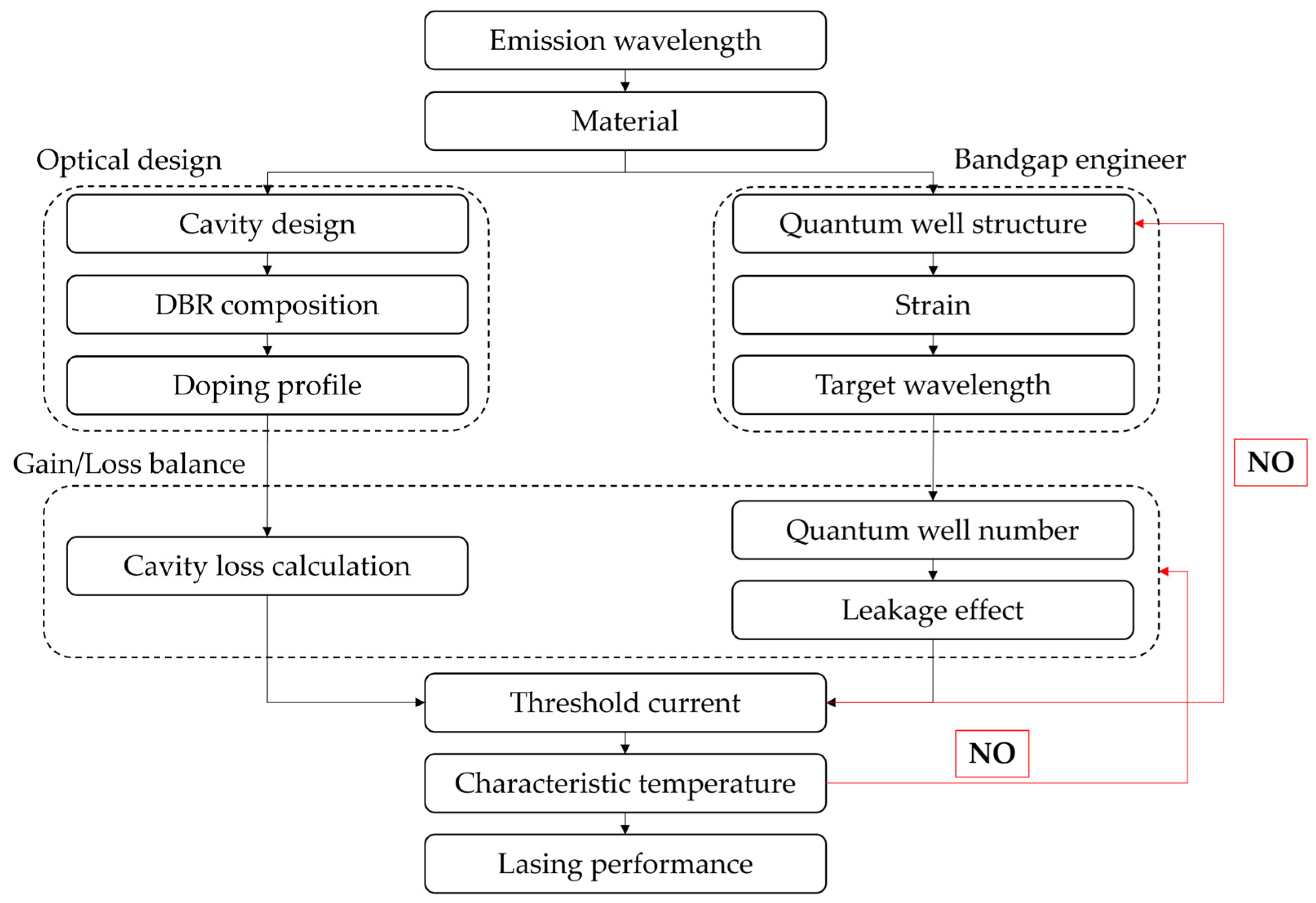
2. Design Flow
3. In AlGaP/InGaP VCSEL Structural Design and Optimization
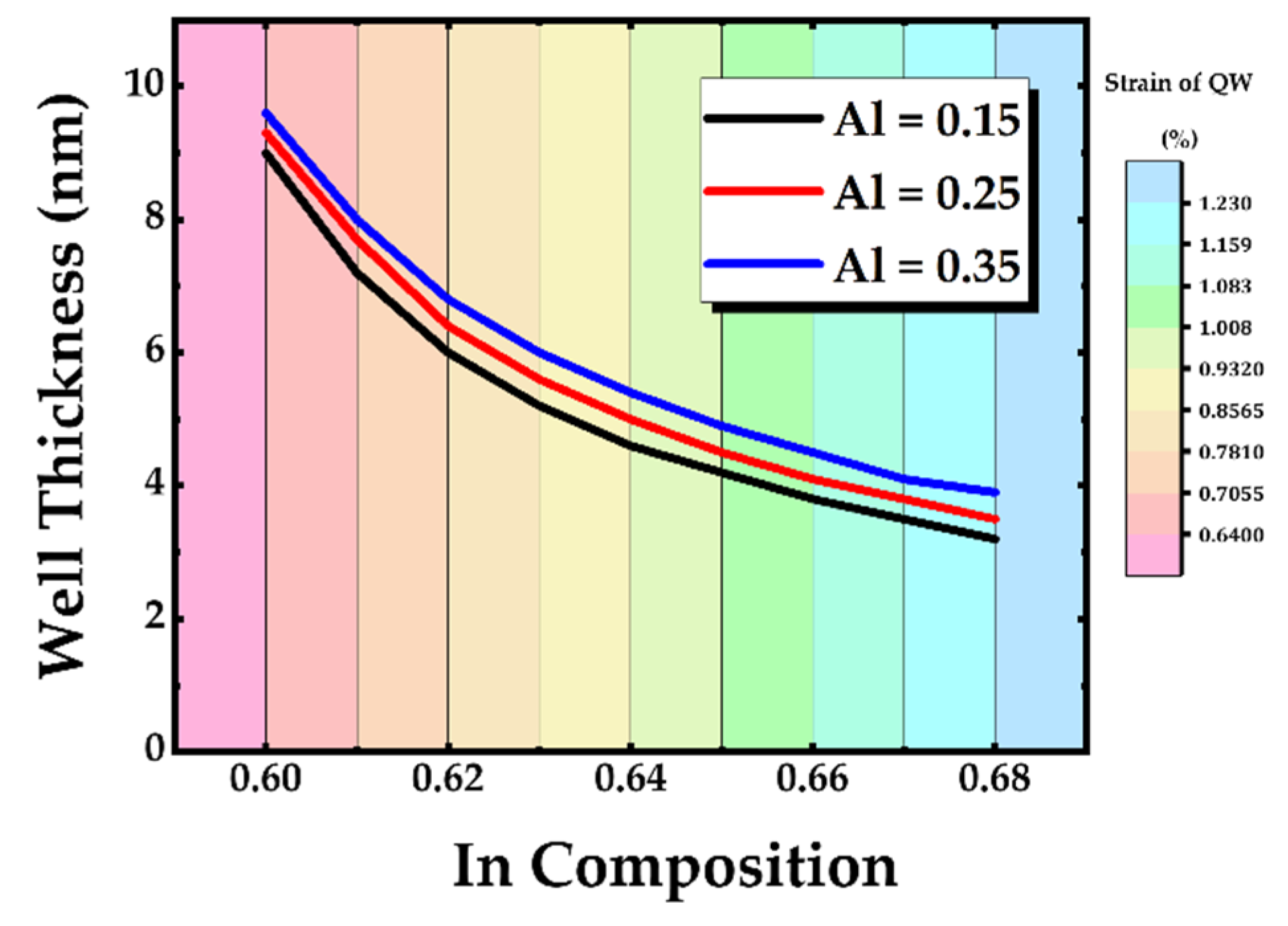
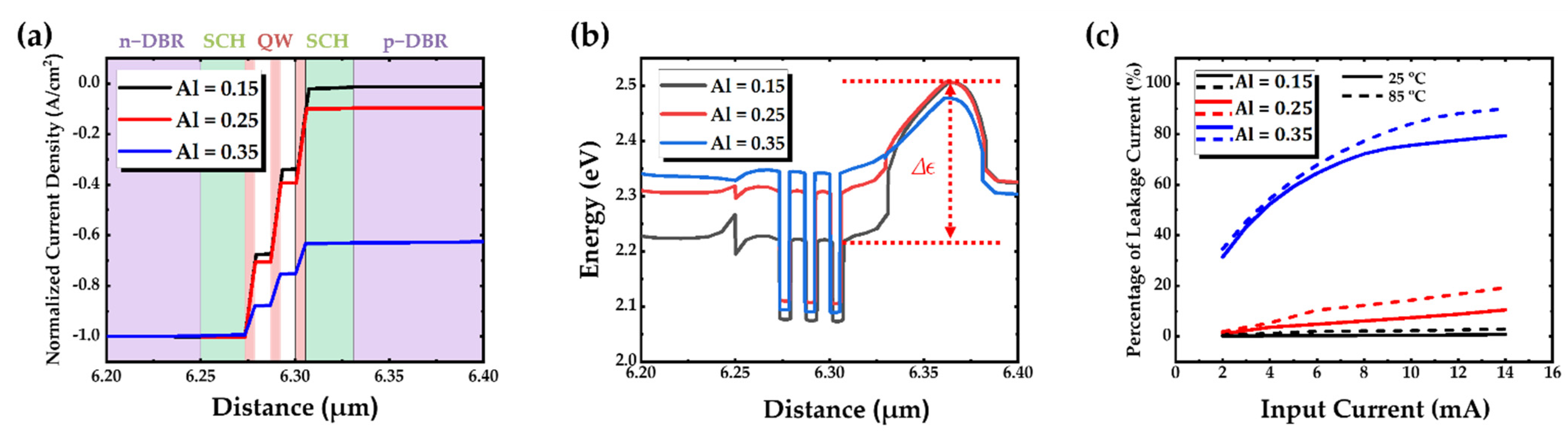
3.1. Leakage Effect
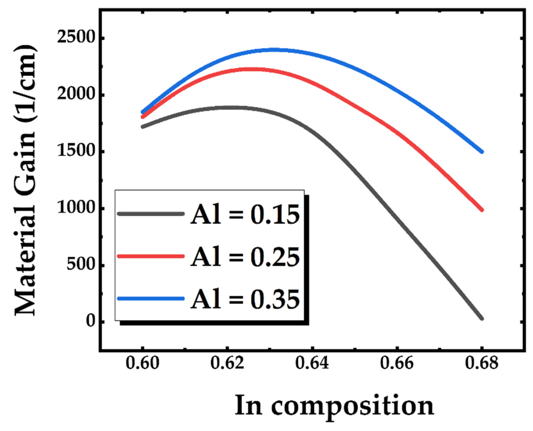
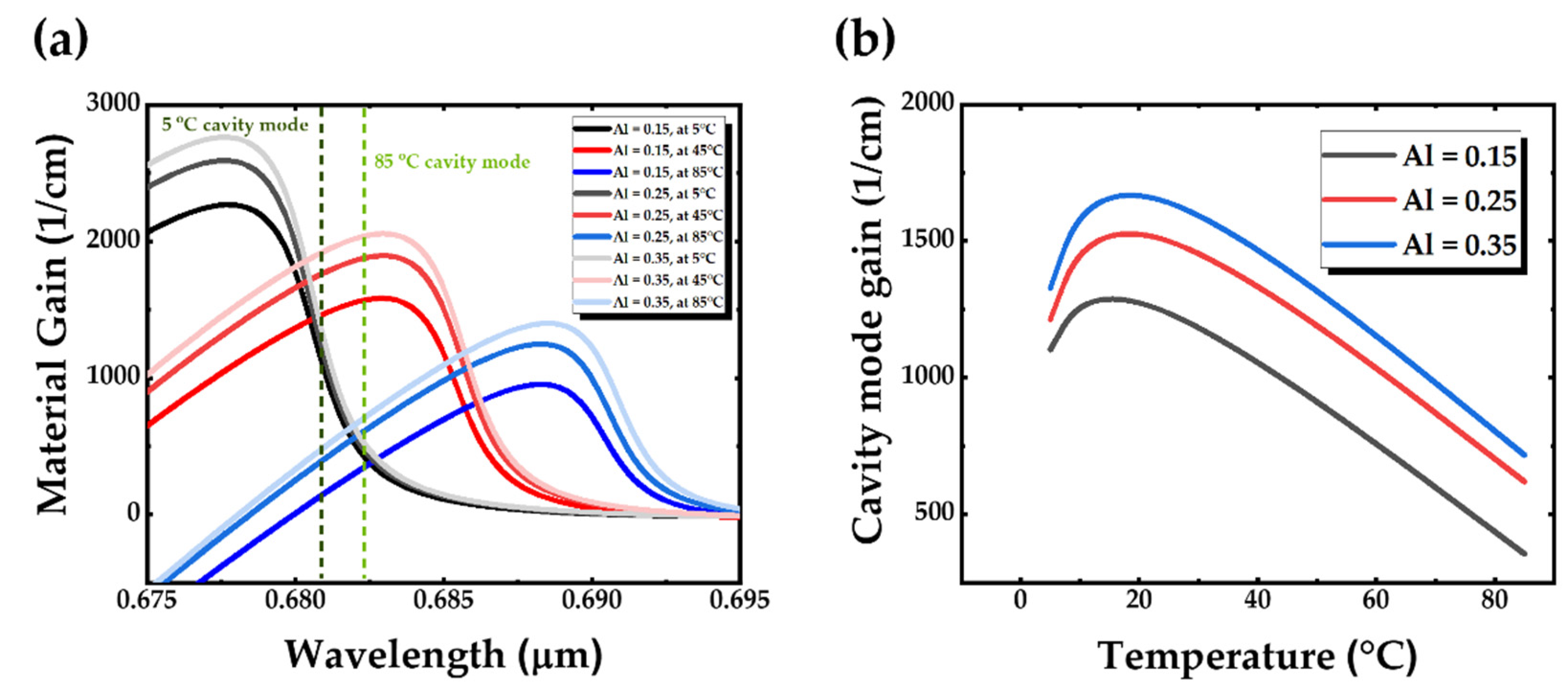
3.2. Temperature Dependence of Optical Gain and Resonance Mode Gain
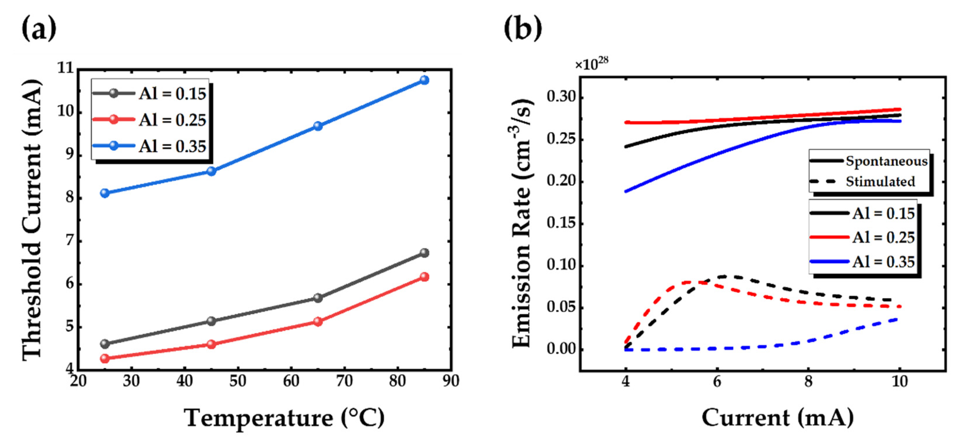
3.3. Threshold Current
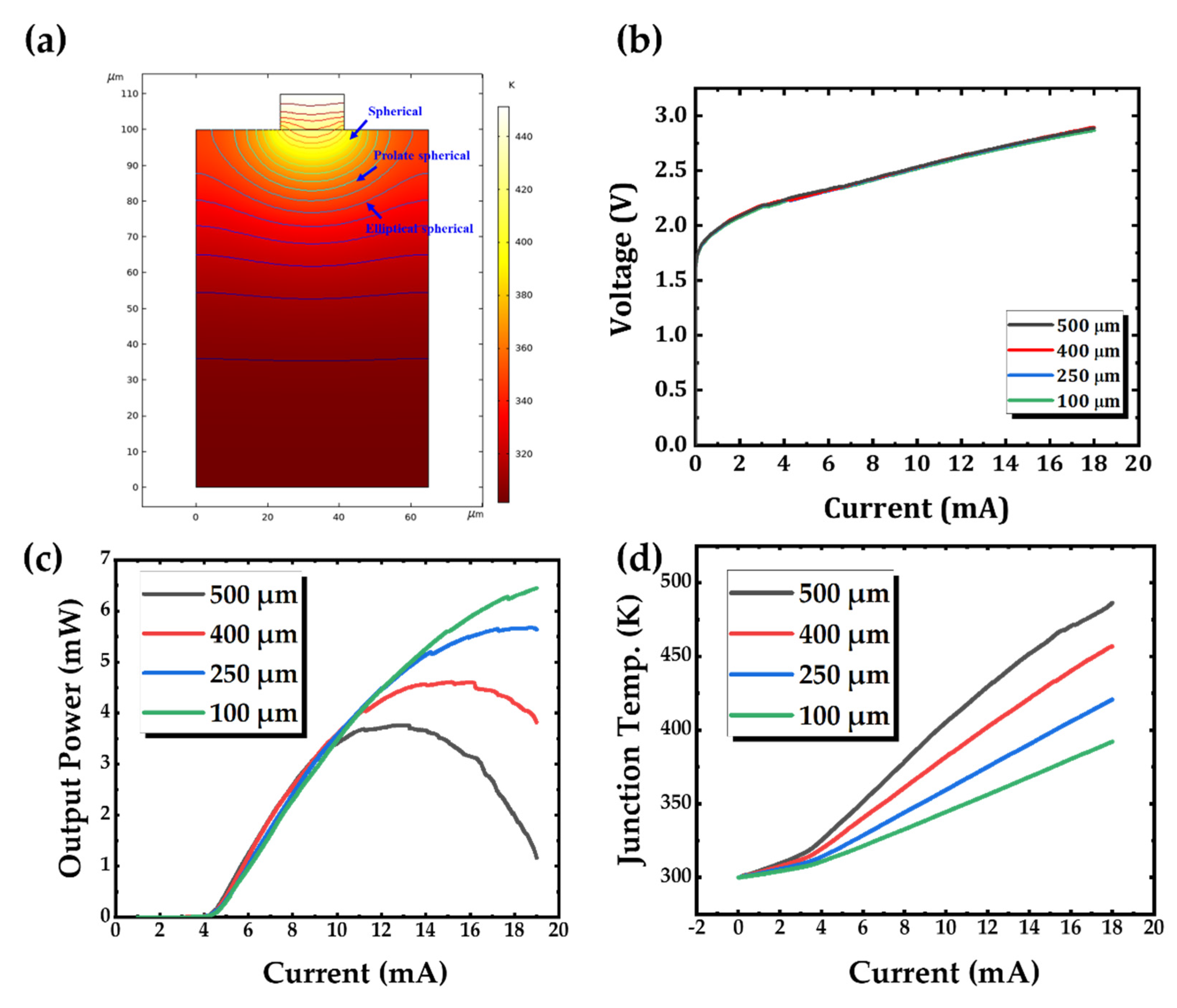
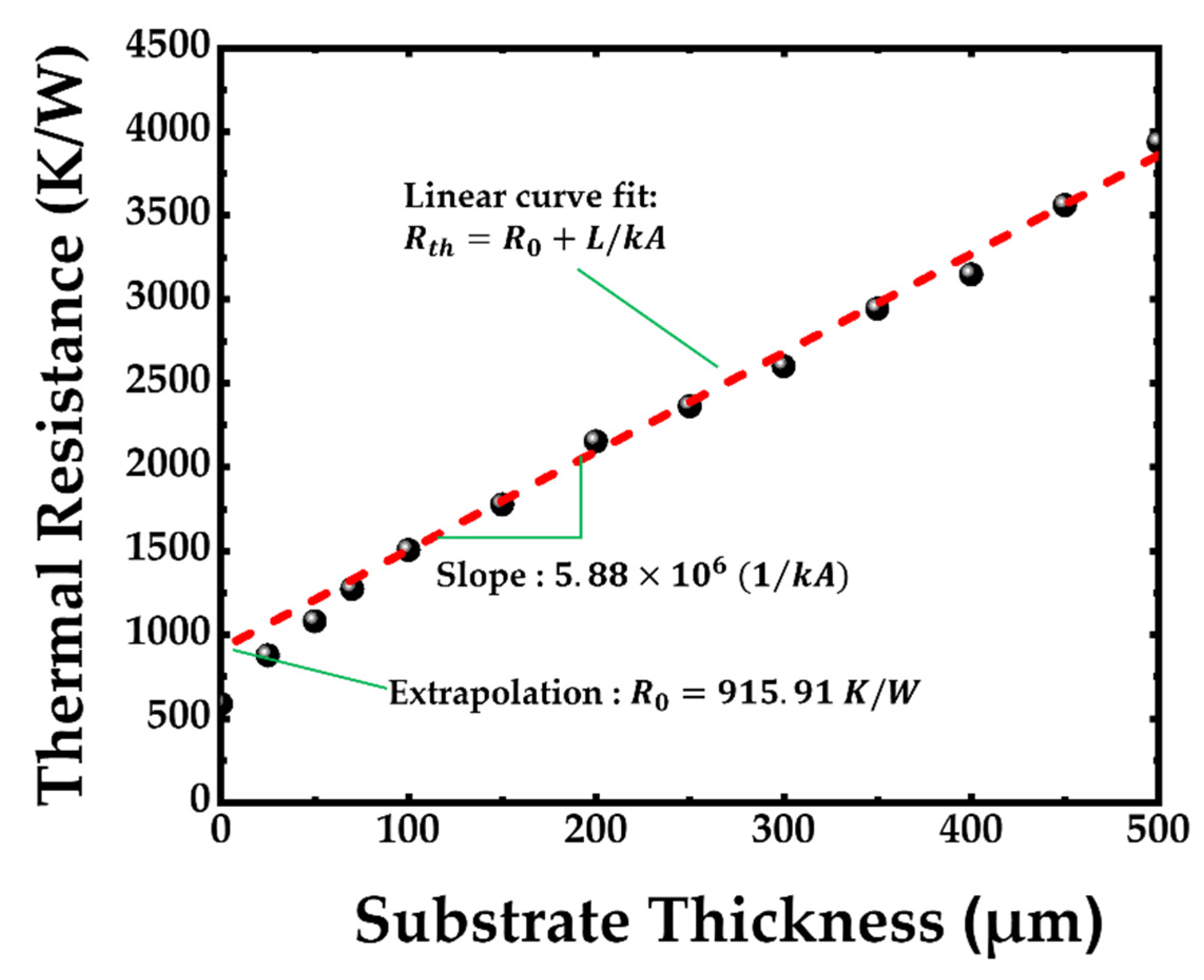
4. Temperature Characteristics of InAlGaP/InGaP VCSEL with Substrates Removal
5. Conclusions
Author Contributions
Funding
Institutional Review Board Statement
Informed Consent Statement
Data Availability Statement
Conflicts of Interest
Appendix A

| Layer | Material | Group | Repeat | Start x | Finish x | Thickness (µm) | Dopant | Type |
|---|---|---|---|---|---|---|---|---|
| 33 | GaAs | 1 | N/A | 0.0150 | 2 × 10²⁰ | p | ||
| 32 | AlxGaAs | 1 | 0.45 | 0.0230 | 1 × 10²⁰ | p | ||
| 31 | AlxGaAs | 1 | 0.88 | 0.45 | 0.0100 | 2 × 10¹⁸ | p | |
| 30 | AlxGaAs | 4 | 37 | 0.88 | 0.0464 | 3 × 10¹⁸ | p | |
| 29 | AlxGaAs | 4 | 37 | 0.45 | 0.88 | 0.0100 | 3 × 10¹⁸ | p |
| 28 | AlxGaAs | 4 | 37 | 0.45 | 0.0431 | 3 × 10¹⁸ | p | |
| 27 | AlxGaAs | 4 | 37 | 0.88 | 0.45 | 0.0100 | 3 × 10¹⁸ | p |
| 26 | AlxGaAs | 1 | 0.88 | 0.0431 | 3 × 10¹⁸ | p | ||
| 25 | AlxGaAs | 1 | 0.45 | 0.88 | 0.0100 | 2 × 10¹⁸ | p | |
| 24 | AlxGaAs | 1 | 0.45 | 0.0280 | 3 × 10¹⁸ | p | ||
| 23 | AlxGaAs | 1 | 0.88 | 0.45 | 0.0100 | 2 × 10¹⁸ | p | |
| 22 | AlxGaAs | 1 | 0.985 | 0.0250 | 3 × 10¹⁸ | p | ||
| 21 | AlxGaAs | 1 | 0.90 | 0.0460 | 3 × 10¹⁸ | p | ||
| 20 | AlxGa1−xInP | 1 | 0.70 | 0.0200 | 1 × 10¹⁸ | p | ||
| 19 | AlxGa1−xInP | 1 | 0.50 | 0.70 | 0.0320 | 1 × 10¹⁸ | p | |
| 18 | AlxGa1−xInP | 1 | 0.50 | 0.0235 | N/A | Undoped | ||
| 17 | InGaP | 1 | N/A | 0.0054 | N/A | Undoped | ||
| 16 | AlxGa1−xInP | 3 | 2 | 0.50 | 0.0080 | N/A | Undoped | |
| 15 | InGaP | 3 | 2 | N/A | 0.0054 | N/A | Undoped | |
| 14 | AlxGa1−xInP | 1 | 0.50 | 0.0235 | N/A | Undoped | ||
| 13 | AlxGa1−xInP | 1 | 0.70 | 0.50 | 0.0500 | 1 × 10¹⁸ | n | |
| 12 | AlxGa1−xInP | 1 | 0.70 | 0.0200 | 1 × 10¹⁸ | n | ||
| 11 | AlxGaAs | 1 | 0.88 | 0.0464 | 2 × 10¹⁸ | n | ||
| 10 | AlxGaAs | 1 | 0.45 | 0.88 | 0.0100 | 2 × 10¹⁸ | n | |
| 9 | AlxGaAs | 2 | 5 | 0.45 | 0.0413 | 2 × 10¹⁸ | n | |
| 8 | AlxGaAs | 2 | 5 | 0.88 | 0.45 | 0.0100 | 2 × 10¹⁸ | n |
| 7 | AlxGaAs | 2 | 5 | 0.88 | 0.0464 | 2 × 10¹⁸ | n | |
| 6 | AlxGaAs | 2 | 5 | 0.45 | 0.88 | 0.0100 | 2 × 10¹⁸ | n |
| 5 | AlxGaAs | 1 | 50 | 0.45 | 0.0413 | 2 × 10¹⁸ | n | |
| 4 | AlxGaAs | 1 | 50 | 0.94 | 0.45 | 0.0100 | 2 × 10¹⁸ | n |
| 3 | AlxGaAs | 1 | 50 | 0.94 | 0.0464 | 2 × 10¹⁸ | n | |
| 2 | AlxGaAs | 1 | 50 | 0.45 | 0.94 | 0.0100 | 2 × 10¹⁸ | n |
| 1 | GaAs | 1 | N/A | 100 | 3 × 10¹⁸ | n | ||
References
- Goto, K. Proposal of Ultrahigh Density Optical Disk System Using a Vertical Cavity Surface Emitting Laser Array. Jpn. J. Appl. Phys. 1998, 37, 2274–2278. [Google Scholar] [CrossRef]
- Goto, K.; Kurihara, K. High speed VCSEL array head for tera byte optical disk. In Proceedings of the Technical Digest. CLEO/Pacific Rim ‘99. Pacific Rim Conference on Lasers and Electro-Optics (Cat. No.99TH8464), Online. 30 August–3 September 1999; Volume 4, pp. 1113–1114. [Google Scholar]
- Moench, H.; Carpaij, M.; Gerlach, P.; Gronenborn, S.; Gudde, R.; Hellmig, J.; Kolb, J.; van der Lee, A. VCSEL-Based Sensors for Distance and Velocity; SPIE: Bellingham, WA, USA, 2016; Volume 9766. [Google Scholar]
- Warren, M.; Carson, R.; Sweatt, W.; Wendt, J.; Nevers, J.; Crawford, M.; Hou, H. VCSEL Applications in Sensors and Microsystems; SPIE: Bellingham, WA, USA, 1998; Volume 3286. [Google Scholar]
- Liverman, S.; Bialek, H.; Natarajan, A.; Wang, A.X. VCSEL Array-Based Gigabit Free-Space Optical Femtocell Communication. J. Lightwave Technol. 2020, 38, 1659–1667. [Google Scholar] [CrossRef]
- Tiberi, M.; Kozlovsky, V. Electron-Beam-Pumped VCSEL Light Source for Projection Display; SPIE: Bellingham, WA, USA, 2005; Volume 5740. [Google Scholar]
- Iga, K. VCSEL—Its conception, development, and future. In Proceedings of the Technical Digest of the Eighteenth Microoptics Conference, Tokyo, Japan, 27–30 October 2013; pp. 1–2. [Google Scholar]
- Seurin, J.-F.; Xu, G.; Miglo, A.; Wang, Q.; Van Leeuwen, R.; Xiong, Y.; Zou, W.-X.; Li, D.; Wynn, J.; Khalfin, V.; et al. High-Power Vertical-Cavity Surface-Emitting Lasers for Solid-State Laser Pumping; SPIE: Bellingham, WA, USA, 2012; Volume 8276. [Google Scholar]
- Hall, R.N.; Fenner, G.E.; Kingsley, J.D.; Soltys, T.J.; Carlson, R.O. Coherent Light Emission From GaAs Junctions. Phys. Rev. Lett. 1962, 9, 366–368. [Google Scholar] [CrossRef]
- Holonyak, N., Jr.; Bevacqua, S.F. Coherent (visible) light emission from Ga(As1−xPx) junctions. Appl. Phys. Lett. 1962, 1, 82–83. [Google Scholar] [CrossRef]
- Alferov, Z.I.; Kazarinov, R. Semiconductor laser with electric pumping. Inventor’s Certificate. U.S.S.R. Patent 1963. [Google Scholar]
- Hayashi, I.; Panish, M.B.; Foy, P.W.; Sumski, S. Junction lasers which operate continuously at room temperature. Appl. Phys. Lett. 1970, 17, 109–111. [Google Scholar] [CrossRef]
- Alferov, Z.I.; Andreev, V.; Garbuzov, D.; Zhilyaev, Y.V.; Morozov, E.; Portnoi, E.; Trofim, V. Investigation of the influence of the AlAs-GaAs heterostructure parameters on the laser threshold current and the realization of continuous emission at room temperature. Sov. Phys. Semicond. 1971, 4, 1573–1575. [Google Scholar]
- Rezek, E.A.; Holonyak, N., Jr.; Vojak, B.A.; Stillman, G.E.; Rossi, J.A.; Keune, D.L.; Fairing, J.D. LPE In1−xGaxP1−zAsz (x∼0.12, z∼0.26) DH laser with multiple thin-layer (<500 Å) active region. Appl. Phys. Lett. 1977, 31, 288–290. [Google Scholar] [CrossRef]
- Holonyak, N., Jr.; Kolbas, R.M.; Dupuis, R.D.; Dapkus, P.D. Room-temperature continuous operation of photopumped MO-CVD AlxGa1−xAs-GaAs-AlxGa1−xAs quantum-well lasers. Appl. Phys. Lett. 1978, 33, 73–75. [Google Scholar] [CrossRef]
- Soda, H.; Iga, K.-i.; Kitahara, C.; Suematsu, Y. GaInAsP/InP Surface Emitting Injection Lasers. Jpn. J. Appl. Phys. 1979, 18, 2329–2330. [Google Scholar] [CrossRef]
- Huffaker, D.L.; Deppe, D.G.; Kumar, K.; Rogers, T.J. Native-oxide defined ring contact for low threshold vertical-cavity lasers. Appl. Phys. Lett. 1994, 65, 97–99. [Google Scholar] [CrossRef]
- Choquette, K.D.; Hou, H.Q. Vertical-cavity surface emitting lasers: Moving from research to manufacturing. Proc. IEEE 1997, 85, 1730–1739. [Google Scholar] [CrossRef]
- Martin, O.J.F.; Bona, G.L.; Wolf, P. Thermal behavior of visible AlGaInP-GaInP ridge laser diodes. IEEE J. Quantum Electron. 1992, 28, 2582–2588. [Google Scholar] [CrossRef]
- Bour, D.P.; Treat, D.W.; Thornton, R.L.; Geels, R.S.; Welch, D.F. Drift leakage current in AlGaInP quantum-well lasers. IEEE J. Quantum Electron. 1993, 29, 1337–1343. [Google Scholar] [CrossRef]
- Knowles, G.; Sweeney, S.; Sale, T. Influence of leakage and gain-cavity alignment on the performance of Al (GaInP) visible vertical-cavity surface emitting lasers. IEEE Proc. Optoelectron. 2001, 148, 55–59. [Google Scholar] [CrossRef]
- Gomyo, A.; Suzuki, T.; Kobayashi, K.; Kawata, S.; Hino, I.; Yuasa, T. Evidence for the existence of an ordered state in Ga0.5In0.5P grown by metalorganic vapor phase epitaxy and its relation to band-gap energy. Appl. Phys. Lett. 1987, 50, 673–675. [Google Scholar] [CrossRef]
- Hiroyama, R.; Hamada, H.; Shono, M.; Honda, S.; Yodoshi, K.; Yamaguchi, T. 630 nm-band AlGaInP strained MQW laser diodes with an MQB grown on misoriented substrates. In Proceedings of the 13th IEEE International Semiconductor Laser Conference, Takamatsu, Japan, 21–25 September 1992; pp. 154–155. [Google Scholar]
- Hamada, H. Characterization of Gallium Indium Phosphide and Progress of Aluminum Gallium Indium Phosphide System Quantum-Well Laser Diode. Materials 2017, 10, 875. [Google Scholar] [CrossRef] [PubMed]
- Piprek, J.; Troger, T.; Schroter, B.; Kolodzey, J.; Ih, C.S. Thermal conductivity reduction in GaAs-AlAs distributed Bragg reflectors. IEEE Photonics Technol. Lett. 1998, 10, 81–83. [Google Scholar] [CrossRef]
- Bhattacharya, A.; Zorn, M.; Oster, A.; Nasarek, M.; Wenzel, H.; Sebastian, J.; Weyers, M.; Tränkle, G. Optimization of MOVPE growth for 650nm-emitting VCSELs. J. Cryst. Growth 2000, 221, 663–667. [Google Scholar] [CrossRef]
- Yao, T. Thermal properties of AlAs/GaAs superlattices. Appl. Phys. Lett. 1987, 51, 1798–1800. [Google Scholar] [CrossRef]
- Chow, W.W.; Choquette, K.D.; Crawford, M.H.; Lear, K.L.; Hadley, G.R. Design, fabrication, and performance of infrared and visible vertical-cavity surface-emitting lasers. IEEE J. Quantum Electron. 1997, 33, 1810–1824. [Google Scholar] [CrossRef]
- Knowles, G.; Sweeney, S.; Sale, T.; Adams, A. Self-heating effects in red (665 nm) VCSELs. IEE Proc. Optoelectron. 2001, 148, 256–260. [Google Scholar] [CrossRef]
- Mutig, A.; Fiol, G.; Potschke, K.; Moser, P.; Arsenijevic, D.; Shchukin, V.A.; Ledentsov, N.N.; Mikhrin, S.S.; Krestnikov, I.L.; Livshits, D.A.; et al. Temperature-Dependent Small-Signal Analysis of High-Speed High-Temperature Stable 980-nm VCSELs. IEEE J. Sel. Top. Quantum Electron. 2009, 15, 679–686. [Google Scholar] [CrossRef]
- Johnson, K.; Hibbs-Brenner, M.; Hogan, W.; Dummer, M. Advances in Red VCSEL Technology. Adv. Opt. Technol. 2012, 2012, 569379. [Google Scholar] [CrossRef]
- Lott, J.; Schneider, R. Electrically injected visible (639–661 nm) vertical cavity surface emitting lasers. Electron. Lett. 1993, 29, 830–832. [Google Scholar] [CrossRef]
- Huang, K.F.; Tai, K.; Wu, C.C.; Wynn, J.D. Continuous wave visible InGaP/InGaAlP quantum-well surface-emitting laser diodes. IEEE Trans. Electron Devices 1993, 40, 2119. [Google Scholar] [CrossRef]
- Katsuyama, T.; Yoshida, I.; Shinkai, J.; Hashimoto, J.; Hayashi, H. Very low threshold current AlGaInP/GaxIn1−xP strained single quantum well visible laser diode. Electron. Lett. 1990, 17, 1375–1377. [Google Scholar] [CrossRef]
- Serreze, H.B.; Chen, Y.C. Low-threshold, strained-layer, GaInP/AlGaInP GRINSCH visible diode lasers. IEEE Photonics Technol. Lett. 1991, 3, 397–399. [Google Scholar] [CrossRef]
- Katsuyama, T.; Yoshida, I.; Shinkai, J.; Hashimoto, J.; Hayashi, H. High temperature (≥150 °C) and low threshold current operation of AlGaInP/GaxIn1−xP strained multiple quantum well visible laser diodes. Appl. Phys. Lett. 1991, 59, 3351–3353. [Google Scholar] [CrossRef]
- Mannoh, M.; Hoshina, J.; Kamiyama, S.; Ohta, H.; Ban, Y.; Ohnaka, K. High power and high-temperature operation of GaInP/AlGaInP strained multiple quantum well lasers. Appl. Phys. Lett. 1993, 62, 1173–1175. [Google Scholar] [CrossRef]
- Blood, P.; Smowton, P. Strain dependence of threshold current in fixed-wavelength GaInP laser diodes. IEEE J. Sel. Top. Quantum Electron. 1995, 1, 707–711. [Google Scholar] [CrossRef]
- Kobayashi, R.; Hotta, H.; Miyasaka, F.; Hara, K.; Kobayashi, K. Low-threshold, highly reliable 630 nm-band AlGaIP visible laser diodes with AlInP buried waveguide. Electron. Lett. 1996, 32, 894–896. [Google Scholar] [CrossRef]
- Watanabe, M.; Matsuura, H.; Shimada, N.; Okuda, H. Optimum tensile-strained multiquantum-well structure of 630-nm band InGaAlP lasers for high temperature and reliable operation. IEEE J. Sel. Top. Quantum Electron. 1995, 1, 712–716. [Google Scholar] [CrossRef]
- Tanaka, T.; Yanagisawa, H.; Kawanaka, S.; Minagawa, S. Study on strain-induced polarization mode of strained-layer quantum-well 630-nm AlGaInP LD’s. IEEE Photonics Technol. Lett. 1995, 7, 136–139. [Google Scholar] [CrossRef]
- Valster, A.; van der Poel, C.J.; Finke, M.N.; Boermans, M.J.B. Effect of strain on the threshold current of GaInP/AlGaInP quantum well lasers emitting at 633 nm. In Proceedings of the 13th IEEE International Semiconductor Laser Conference, Kagazwa, Japan, 21–25 September 1992; pp. 152–153. [Google Scholar]
- Kamiyama, S.; Uenoyama, T.; Mannoh, M.; Ohnaka, K. Strain Effect on 630 nm GaInP/AlGaInP Multi-Quantum Well Lasers. Jpn. J. Appl. Phys. 1994, 33, 2571–2578. [Google Scholar] [CrossRef]
- Kamiyama, S.; Monnoh, M.; Ohnaka, K.; Uenoyama, T. Studies of threshold current dependence on compressive and tensile strain of 630 nm GaInP/AlGaInP multi-quantum-well lasers. J. Appl. Phys. 1994, 75, 8201–8203. [Google Scholar] [CrossRef]
- Smowton, P.; Summers, H.; Rees, P.; Blood, P. Optimization of 670-nm Strained Quantum well Laser Diodes; SPIE: Bellingham, WA, USA, 1994; Volume 2148. [Google Scholar]
- Hiroyama, R.; Bessho, Y.; Kase, H.; Ikegami, T.; Honda, S.; Shono, M.; Yodoshi, K.; Yamaguchi, T.; Niina, T. Strain-compensated multiple quantum well 630-nm-band AlGaInP laser diodes. In Proceedings of the IEEE 14th International Semiconductor Laser Conference, Maui, HI, USA, 19–23 September 1994; pp. 205–206. [Google Scholar]
- Valster, A.; Meney, A.T.; Downes, J.R.; Faux, D.A.; Adams, A.R.; Brouwer, A.A.; Corbijn, A.J. Strain-overcompensated GaInP-AlGaInP quantum-well laser structures for improved reliability at high-output powers. IEEE J. Sel. Top. Quantum Electron. 1997, 3, 180–187. [Google Scholar] [CrossRef]
- Tansu, N.; Zhou, D.; Mawst, L.J. Low-temperature sensitive, compressively strained InGaAsP active (/spl lambda/= 0.78–0.85 μm) region diode lasers. IEEE Photonics Technol. Lett. 2000, 12, 603–605. [Google Scholar] [CrossRef]
- Yu, Y.; Zhang, X.; Huang, B.; Wang, D.; Wei, J.; Zhou, H.; Pan, J.; Qi, Y.; Chen, W.; Qin, X.; et al. Strain effect and characteristics of GaInP/AlGaInP strain-compensated multiple quantum wells. Mater. Sci. Eng. B 2003, 97, 211–216. [Google Scholar] [CrossRef]
- Schneider, R.P., Jr.; Crawford, M.H.; Choquette, K.D.; Lear, K.L.; Kilcoyne, S.P.; Figiel, J.J. Improved AlGaInP-based red (670–690 nm) surface-emitting lasers with novel C-doped short-cavity epitaxial design. Appl. Phys. Lett. 1995, 67, 329–331. [Google Scholar] [CrossRef]
- Ohba, Y.; Nishikawa, Y.; Nozaki, C.; Sugawara, H.; Nakanisi, T. A study of p-type doping for AlGaInP grown by low-pressure MOCVD. J. Cryst. Growth 1988, 93, 613–617. [Google Scholar] [CrossRef]
- Huang, M.-F.; Tsai, M.-L.; Kuo, Y.-K. Improvement of Characteristic Temperature for AlGaInP Laser Diodes; SPIE: Bellingham, WA, USA, 2005; Volume 5628. [Google Scholar]
- Huang, M.-F.; Sun, Y.-L. Optimization of Barrier Structure for Strain-Compensated Multiple-Quantum-Well AlGaInP Laser Diodes. Jpn. J. Appl. Phys. 2006, 45, 7600–7604. [Google Scholar] [CrossRef]
- Huang, M.F.; Tsai, M.L.; Shin, J.Y.; Sun, Y.L.; Yang, R.M.; Kuo, Y.K. Optimization of active layer structures to minimize leakage current for an AlGaInP laser diode. Appl. Phys. A 2005, 81, 1369–1373. [Google Scholar] [CrossRef]
- Onischenko, A.; Sale, T.; O’Reilly, E.; Adams, A.; Pinches, S.; Frost, J.; Woodhead, J. Progress in the design and development of AlGaInP visible VCSELs. IEE Proc. Optoelectron. 2000, 147, 15–21. [Google Scholar] [CrossRef]
- Zappe, H. Laser Diode Microsystems; Springer Science & Business Media: Berlin, Germany, 2004. [Google Scholar]
- Iga, K. Surface-emitting laser-its birth and generation of new optoelectronics field. IEEE J. Sel. Top. Quantum Electron. 2000, 6, 1201–1215. [Google Scholar] [CrossRef]
- Linnik, M.; Christou, A. Group III-Nitride Based VCSEL for Applications at the Wavelength of 400nm. MRS Online Proc. Libr. 2001, 639, 642. [Google Scholar] [CrossRef]
- Tsai, C.T.; Peng, C.Y.; Wu, C.Y.; Leong, S.F.; Kao, H.Y.; Wang, H.Y.; Chen, Y.W.; Weng, Z.K.; Chi, Y.C.; Kuo, H.C.; et al. Multi-Mode VCSEL Chip with High-Indium-Density InGaAs/AlGaAs Quantum-Well Pairs for QAM-OFDM in Multi-Mode Fiber. IEEE J. Quantum Electron. 2017, 53, 1–8. [Google Scholar] [CrossRef]
- Casey, H.C.; Panish, M.B. Heterostructure Lasers; Academic Press: Cambridge, MA, USA, 1978; Volume 1. [Google Scholar]
- Mitin, V.; Kochelap, V.; Stroscio, M.A. Quantum Heterostructures: Microelectronics and Optoelectronics; Cambridge University Press: Cambridge, UK, 1999. [Google Scholar]
- Merzbacher, E. Quantum Mechanics; Jones & Bartlett Publishers: Burlington, MA, USA, 1961. [Google Scholar]
- Wooten, F. Optical Properties of Solids. Am. J. Phys. 1973, 41, 939–940. [Google Scholar] [CrossRef]
- Zielinski, E.; Schweizer, H.; Hausser, S.; Stuber, R.; Pilkuhn, M.; Weimann, G. Systematics of laser operation in GaAs/AlGaAs multiquantum well heterostructures. IEEE J. Quantum Electron. 1987, 23, 969–976. [Google Scholar] [CrossRef]
- Zielinski, E.; Keppler, F.; Hausser, S.; Pilkuhn, M.H.; Sauer, R.; Tsang, W.T. Optical gain and loss processes in GaInAs/InP MQW laser structures. IEEE J. Quantum Electron. 1989, 25, 1407–1416. [Google Scholar] [CrossRef]
- Asada, M.; Kameyama, A.; Suematsu, Y. Gain and intervalence band absorption in quantum-well lasers. IEEE J. Quantum Electron. 1984, 20, 745–753. [Google Scholar] [CrossRef]
- Chuang, S.L. Physics of Photonic Devices; John Wiley & Sons: Hoboken, NJ, USA, 2012. [Google Scholar]
- Hagen, S.H.; Valster, A.; Boermans, M.J.B.; van der Heyden, J. Investigation of the temperature dependence of the threshold current density of GaInP/AlGaInP double-heterostructure lasers. Appl. Phys. Lett. 1990, 57, 2291–2293. [Google Scholar] [CrossRef]
- Yu, S.F. Analysis and Design of Vertical Cavity Surface Emitting Lasers; John Wiley & Sons: Hoboken, NJ, USA, 2003; Volume 7. [Google Scholar]
- Bastard, G.; Mendez, E.E.; Chang, L.L.; Esaki, L. Variational calculations on a quantum well in an electric field. Phys. Rev. B 1983, 28, 3241–3245. [Google Scholar] [CrossRef]
- Vignaud, D.; Mollot, F. Conduction band offset in the AlxGayIn1−x−yP/Ga0.52In0.48P system as studied by luminescence spectroscopy. J. Appl. Phys. 2003, 93, 384–389. [Google Scholar] [CrossRef]
- Choi, J.H.; Wang, L.; Bi, H.; Chen, R.T. Effects of Thermal-Via Structures on Thin-Film VCSELs for Fully Embedded Board-LevelOptical Interconnection System. IEEE J. Sel. Top. Quantum Electron. 2006, 12, 1060–1065. [Google Scholar] [CrossRef]
- Kuo, Y.K.; Chen, J.R.; Chen, M.L.; Liou, B.T. Numerical study on strained InGaAsP/InGaP quantum wells for 850-nm vertical-cavity surface-emitting lasers. Appl. Phys. B 2007, 86, 623–631. [Google Scholar] [CrossRef]
- Yum, W.-S.; Lee, S.-Y.; Kim, M.-S.; Yoon, S.-J.; Oh, J.-T.; Jeong, H.-H.; Seong, T.-Y. Improving Performance of GaAs-Based Vertical-Cavity Surface-Emitting Lasers by Employing Thermally Conductive Metal Substrate. ECS J. Solid State Sci. Technol. 2021, 10, 015001. [Google Scholar] [CrossRef]
- Chen, R.T.; Lei, L.; Chulchae, C.; Liu, Y.J.; Bihari, B.; Wu, L.; Tang, S.; Wickman, R.; Picor, B.; Hibb-Brenner, M.K.; et al. Fully embedded board-level guided-wave optoelectronic interconnects. Proc. IEEE 2000, 88, 780–793. [Google Scholar] [CrossRef]
- Vermeersch, B.; De Mey, G. Influence of substrate thickness on thermal impedance of microelectronic structures. Microelectron. Reliab. 2007, 47, 437–443. [Google Scholar] [CrossRef][Green Version]
- Chulchae, C.; Lei, L.; Yujie, L.; Chen, R.T. Performance analysis of 10-μm-thick VCSEL array in fully embedded board level guided-wave optoelectronic interconnects. J. Lightwave Technol. 2003, 21, 1531–1535. [Google Scholar] [CrossRef]
- Wang, L.; Choi, J.; Wang, X.; Chen, R.; Hass, D.; Magera, J. Thin Film Optical Waveguide and Optoelectronic Device Integration for Fully Embedded Board Level Optical Interconnects; SPIE: Bellingham, WA, USA, 2004; Volume 5556. [Google Scholar]
- Seurin, J.-F.; Xu, G.; Khalfin, V.; Miglo, A.; Wynn, J.; Pradhan, P.; Ghosh, C.; D’Asaro, L.A. Progress in High-Power High-Efficiency VCSEL Arrays; SPIE: Bellingham, WA, USA, 2009; Volume 7229. [Google Scholar]
- Hong, K.-B.; Huang, W.-T.; Chung, H.-C.; Chang, G.-H.; Yang, D.; Lu, Z.-K.; Chen, S.-L.; Kuo, H.-C. High-Speed and High-Power 940 nm Flip-Chip VCSEL Array for LiDAR Application. Crystals 2021, 11, 1237. [Google Scholar] [CrossRef]


Publisher’s Note: MDPI stays neutral with regard to jurisdictional claims in published maps and institutional affiliations. |
© 2022 by the authors. Licensee MDPI, Basel, Switzerland. This article is an open access article distributed under the terms and conditions of the Creative Commons Attribution (CC BY) license (https://creativecommons.org/licenses/by/4.0/).
Share and Cite
Peng, C.-Y.; Huang, W.-T.; Lu, Z.-K.; Chen, S.-C.; Kuo, H.-C. Design of High-Power Red VCSEL on a Removable Substrate. Photonics 2022, 9, 763. https://doi.org/10.3390/photonics9100763
Peng C-Y, Huang W-T, Lu Z-K, Chen S-C, Kuo H-C. Design of High-Power Red VCSEL on a Removable Substrate. Photonics. 2022; 9(10):763. https://doi.org/10.3390/photonics9100763
Chicago/Turabian StylePeng, Chun-Yen, Wei-Ta Huang, Zhi-Kuang Lu, Shih-Chen Chen, and Hao-Chung Kuo. 2022. "Design of High-Power Red VCSEL on a Removable Substrate" Photonics 9, no. 10: 763. https://doi.org/10.3390/photonics9100763
APA StylePeng, C.-Y., Huang, W.-T., Lu, Z.-K., Chen, S.-C., & Kuo, H.-C. (2022). Design of High-Power Red VCSEL on a Removable Substrate. Photonics, 9(10), 763. https://doi.org/10.3390/photonics9100763