Effect of Transmission-Line Contact Length on the 50-Gbit/s Data Encoding Performance of a Multimode VCSEL

 ,
, 
Abstract
1. Introduction
2. Experimental Setup
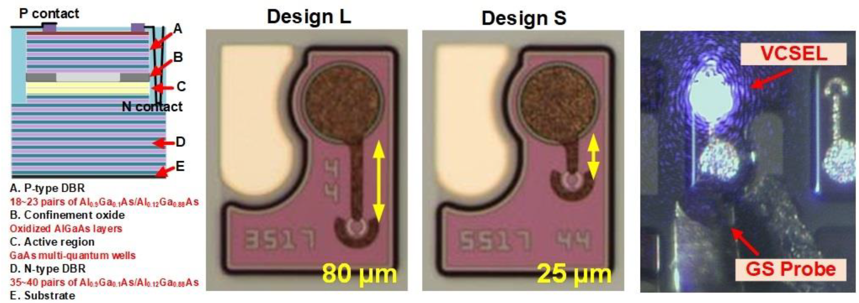
2.1. Oxide Confined MM-VCSEL with Transmission Microstrip
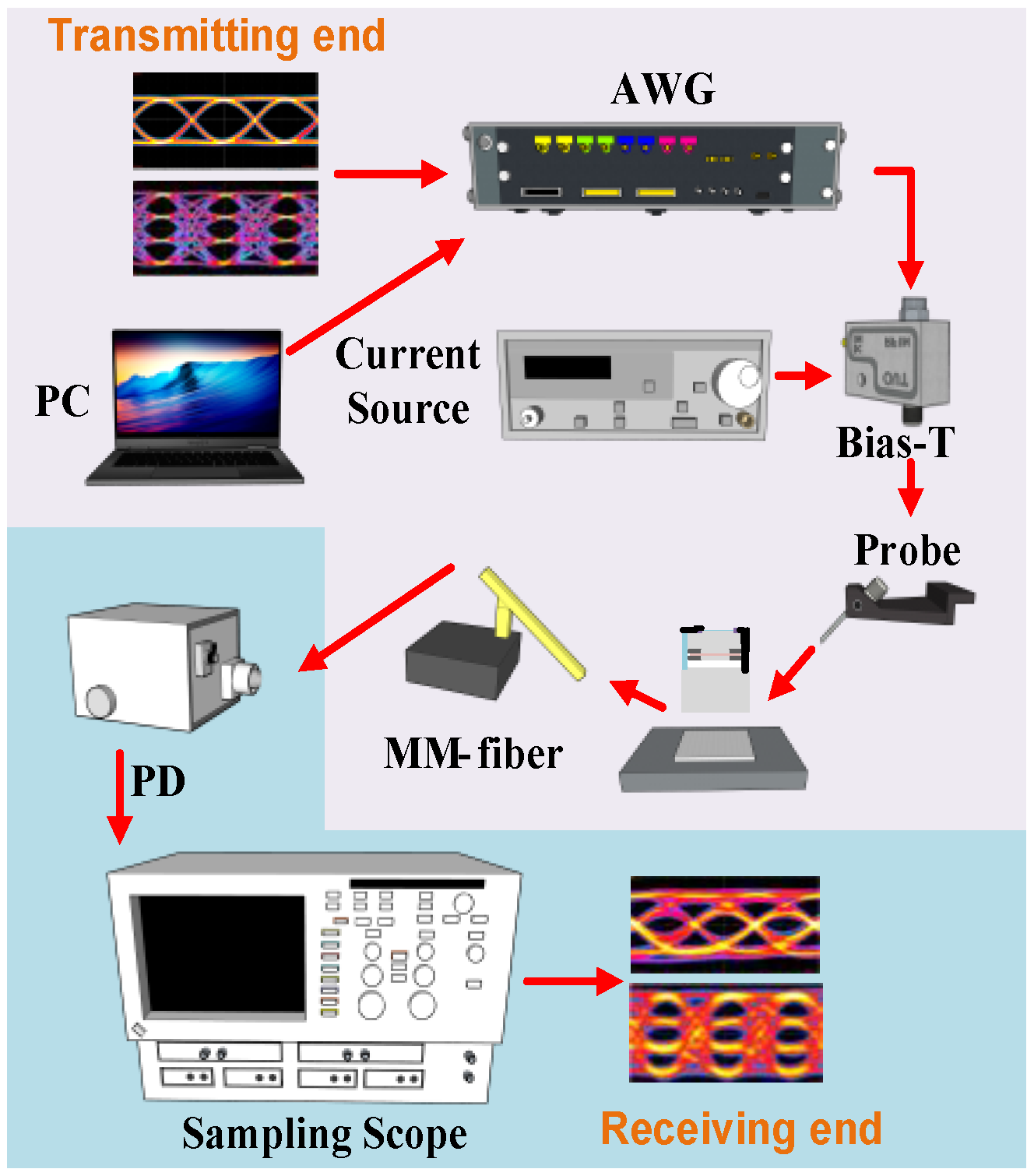
2.2. Experimental Setup of the Data Transmission System
3. Results
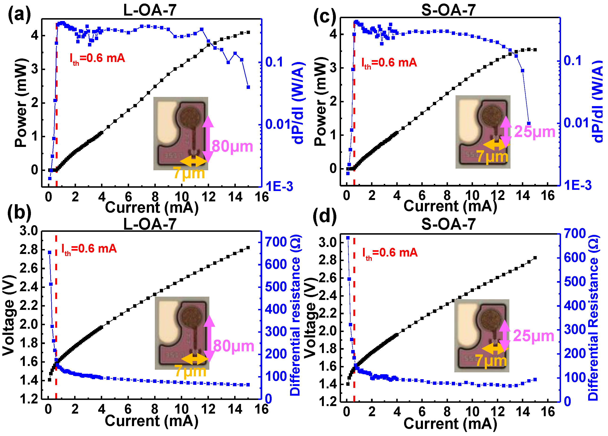
3.1. Characteristics of MM-VCSELs in Four Designs
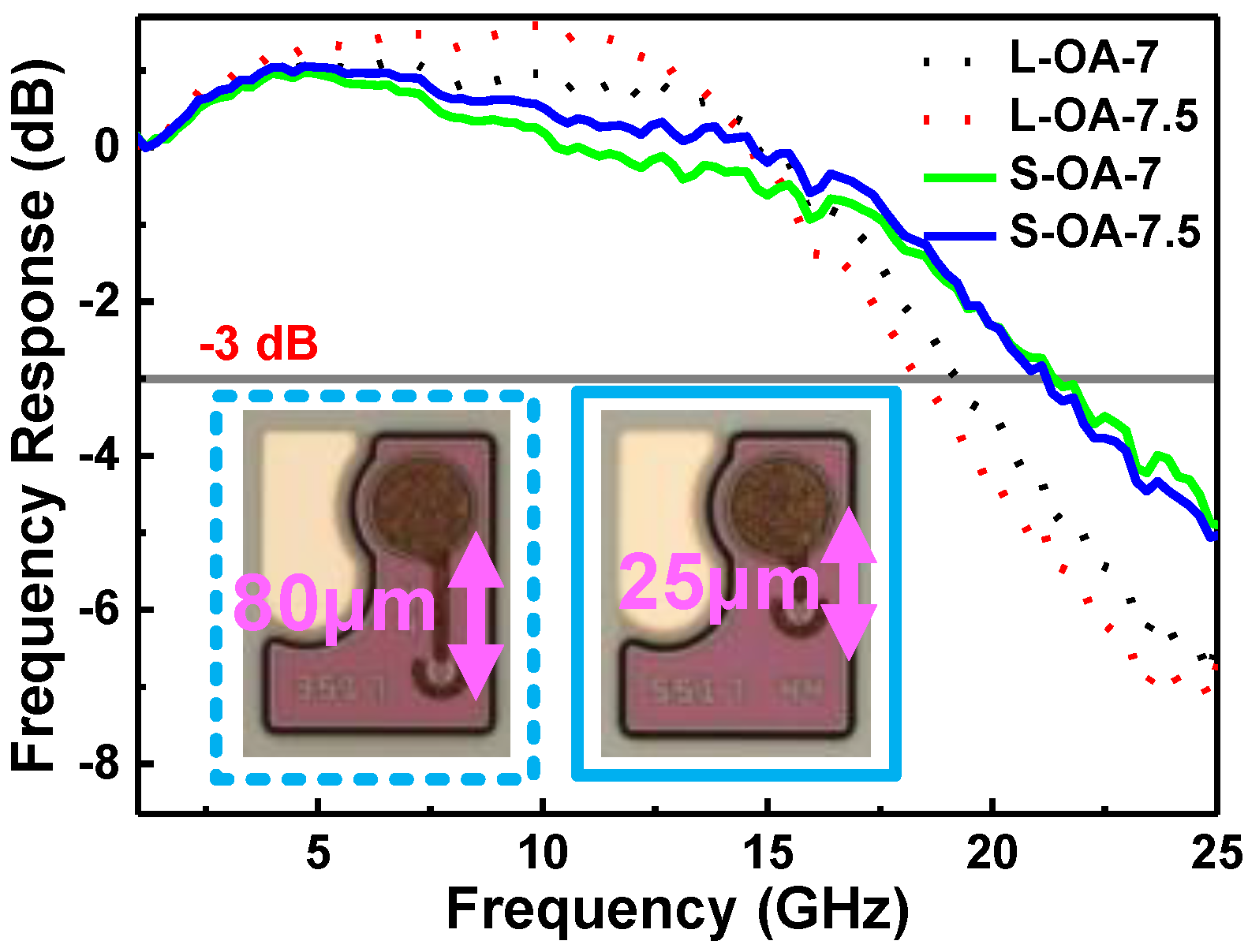
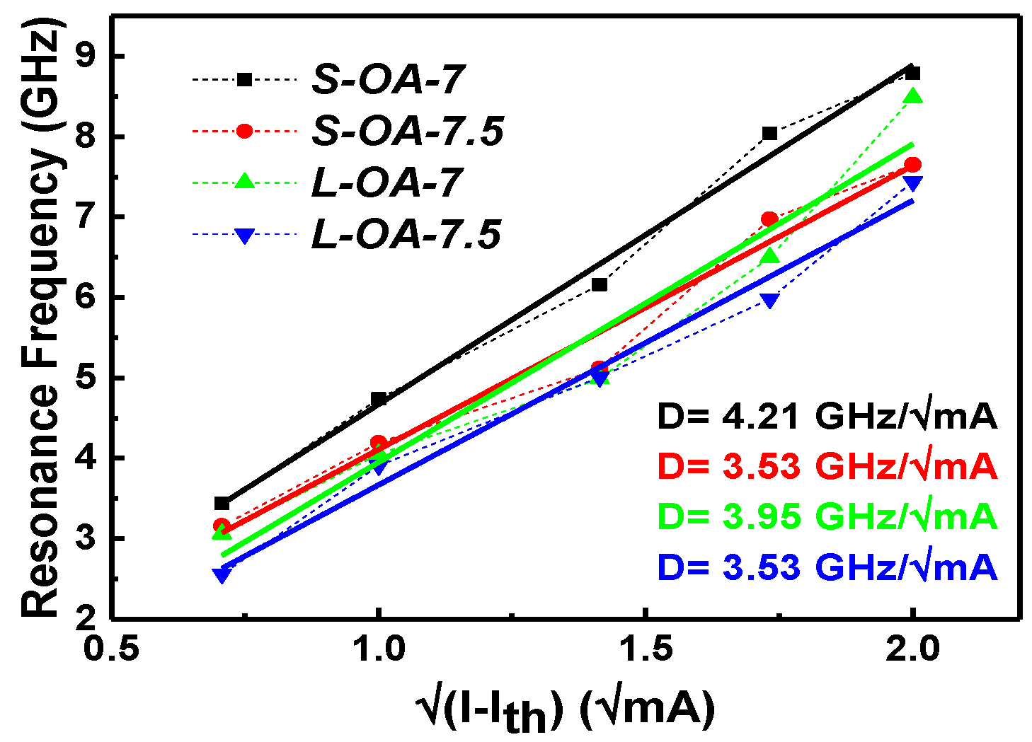
3.2. Modulation Responses of the MM-VCSELs
3.3. Bias Current Optimization for High-Speed Transmission
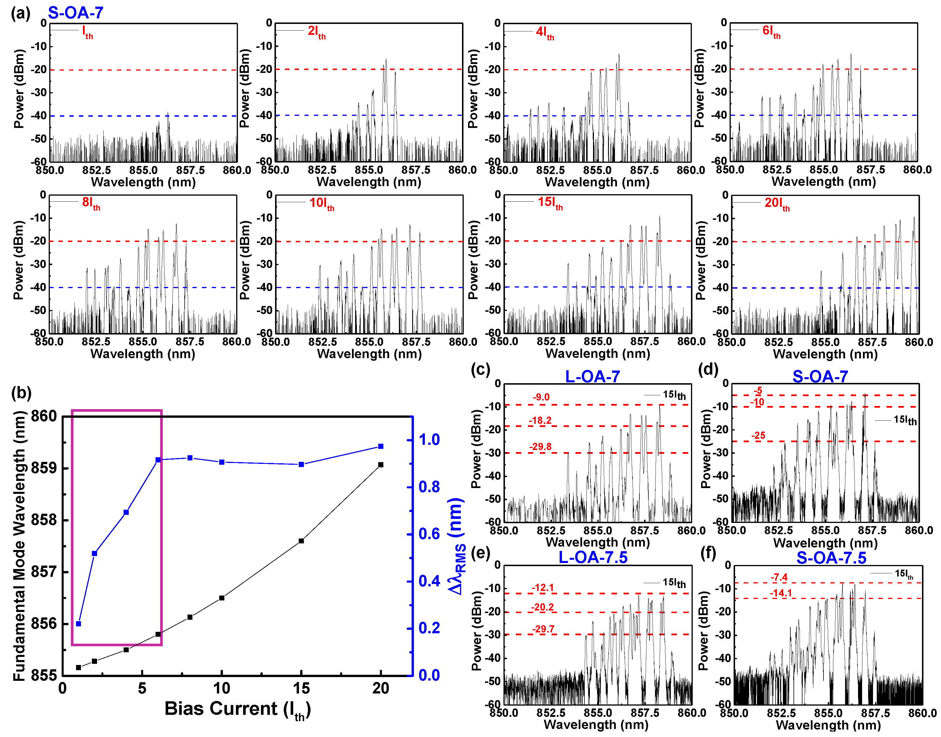
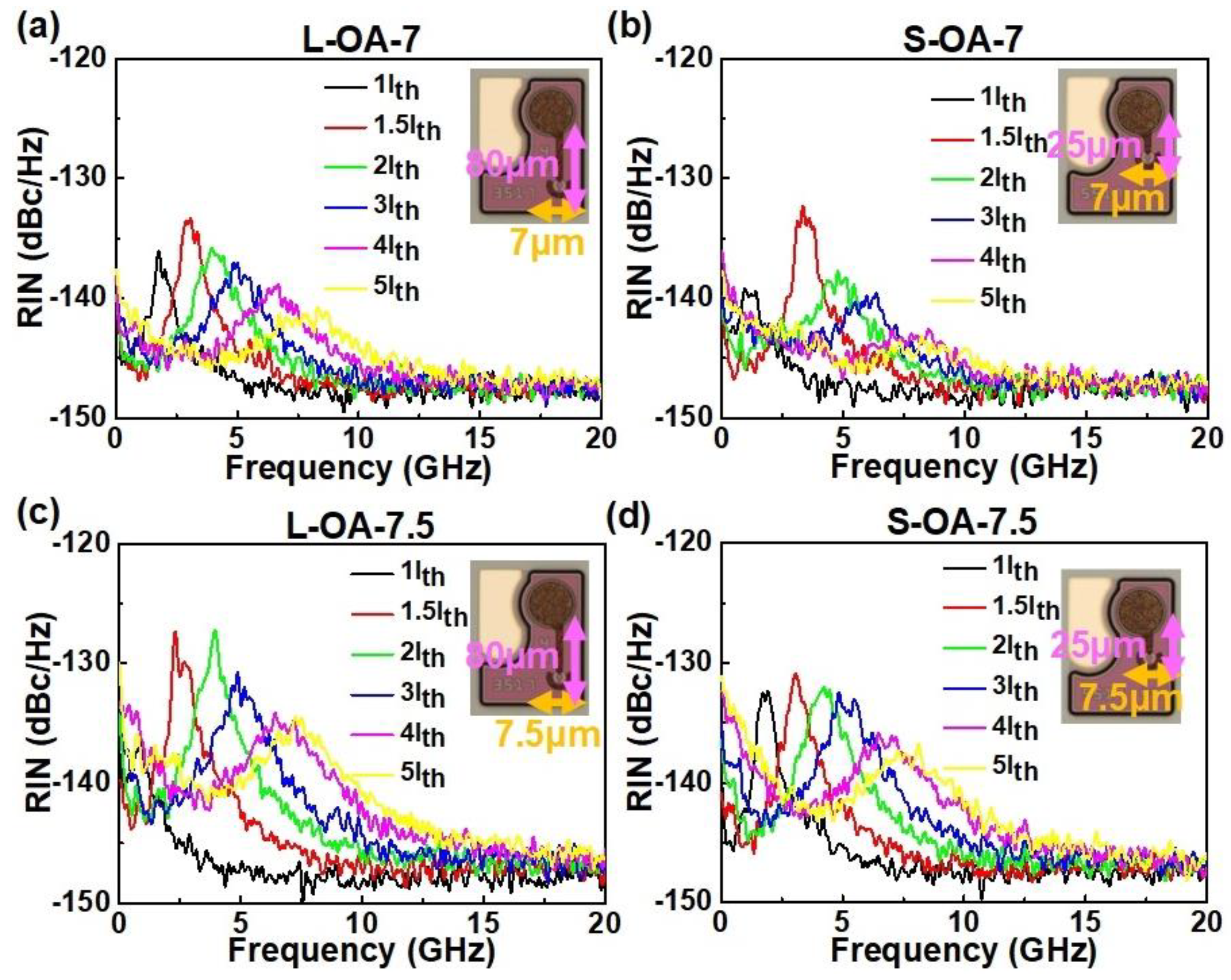
3.4. RIN and MPN of the MM-VCSELs with Different Designs
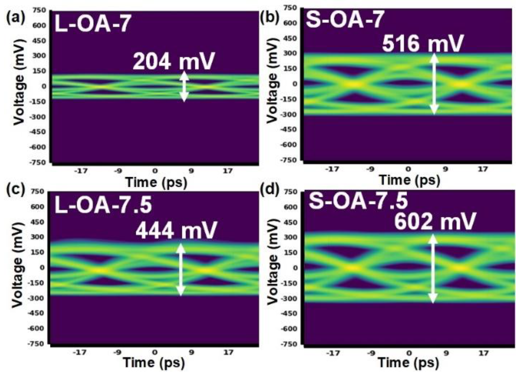
3.5. Transmission Performances in the MM-VCSELs with Four Designs
4. Conclusions
Author Contributions
Funding
Institutional Review Board Statement
Informed Consent Statement
Data Availability Statement
Conflicts of Interest
References
- Cisco Annual Internet Report (2018–2023) White Paper. Available online: http://www.cisco.com/c/en/us/solutions/collateral/executive-perspectives/annual-internet-report/white-paper-c11-741490.html (accessed on 9 March 2020).
- Mutig, A. High Speed VCSELs for Optical Interconnects. Ph.D. Thesis, Technische Universität Berlin, Berlin, Germany, 2010. [Google Scholar]
- Huang, C.-Y.; Wang, H.-Y.; Wu, C.-H.; Cheng, C.-H.; Tsai, C.-T.; Wu, C.-H.; Feng, M.; Lin, G.-R. Comparison of high-speed PAM4 and QAM-OFDM data transmission using single-mode VCSEL in OM5 and OM4 MMF links. IEEE J. Sel. Top. Quantum Electron. 2020, 26, 1500210. [Google Scholar] [CrossRef]
- Kao, H.-Y.; Tsai, C.-T.; Chi, Y.-C.; Peng, C.-Y.; Leong, S.-F.; Wang, H.-Y.; Cheng, C.-H.; Wu, W.-L.; Kuo, H.-C.; Cheng, W.-H.; et al. Long-term thermal stability of single-mode VCSEL under 96-Gbit/s OFDM transmission. IEEE J. Sel. Top. Quantum Electron. 2019, 25, 1500609. [Google Scholar] [CrossRef]
- Li, M.; Chen, X.; Li, K.; Hurley, J.E.; Stone, J. Optical fiber for 1310 nm single-mode and 850 nm few-mode transmission. Proc. SPIE 2019, 10945, 1094503. [Google Scholar]
- Wang, H.L.; Qiu, J.; Yu, X.; Fu, W.; Feng, M. The Modal Effect of VCSELs on Transmitting Data Rate Over Distance in OM4 Fiber. IEEE J. Quantum Electron. 2020, 56, 8000106. [Google Scholar] [CrossRef]
- Westbergh, P.; Gustavsson, J.S.; Haglund, Å.; Larsson, A.; Hopfer, F.; Fiol, G.; Bimberg, D.; Joel, A. 32 Gbit/s multimode fibre transmission using high-speed, low current density 850 nm VCSEL. Electron. Lett. 2009, 45, 366–368. [Google Scholar] [CrossRef]
- Blokhin, S.A.; Lott, J.A.; Mutig, A.; Fiol, G.; Ledentsov, N.N.; Maximov, M.V.; Nadtochiy, A.M.; Shchukin, V.A.; Bimberg, D. Oxide-confined 850 nm VCSELs operating at bit rates up to 40 Gbit/s. Electron. Lett. 2009, 45, 501–503. [Google Scholar] [CrossRef]
- Lin, Y.-H.; Tsai, C.-T.; Wu, W.-L.; Cheng, C.-H.; Choquette, K.D.; Lin, G.-R. Photonic Crystal Structured Multimode VCSELs Enabling 92-Gbit/s QAM-OFDM Transmission. J. Lightwave Technol. 2021, 39, 4331–4340. [Google Scholar] [CrossRef]
- Huang, C.-Y.; Tsai, C.-T.; Weng, J.-H.; Cheng, C.-H.; Wang, H.-Y.; Wu, C.-H.; Feng, M.; Lin, G.-R. Temperature and Noise Dependence of Tri-Mode VCSEL Carried 120-Gbit/s QAM-OFDM Data in Back-to-Back and OM5-MMF Links. J. Lightwave Technol. 2020, 38, 6746–6758. [Google Scholar] [CrossRef]
- 800G Specification-Ethernet Technology Consortium. Available online: https://ethernettechnologyconsortium.org/wp-content/uploads/2020/03/800G-Specification_r1.0.pdf (accessed on 10 March 2020).
- Hansing, C.C.; Deng, H.; Huffaker, D.L.; Deppe, D.G. Low-threshold continuous-wave surface emitting lasers with etched-void confinement. IEEE Photon. Technol. Lett. 1994, 6, 320–322. [Google Scholar] [CrossRef]
- Huffaker, D.L.; Deppe, D.G.; Kumar, K.; Rogers, T.J. Native-oxide defined ring contact for low-threshold vertical-cavity lasers. Appl. Phys. Lett. 1994, 65, 97–99. [Google Scholar] [CrossRef]
- Hayashi, Y.; Mukaihara, T.; Hatori, N.; Ohnoki, N.; Matsutani, A.; Koyama, F.; Iga, K. Record low-threshold index-guided InGaAs/GaAlAs vertical-cavity surface-emitting laser with a native oxide confinement structure. Electron. Lett. 1995, 31, 560–561. [Google Scholar] [CrossRef]
- Chow, W.W.; Choquette, K.D.; Crawford, M.H.; Lear, K.L.; Hadley, G.R. Design, fabrication, and performance of infrared and visible vertical-cavity surface emitting lasers. IEEE J. Quantum Electron. 1997, 33, 1810–1823. [Google Scholar] [CrossRef]
- Feng, M.; Wu, C.H.; Holonyak, N. Oxide-confined VCSELs for high-speed optical interconnects. IEEE J. Quantum Electron. 2018, 54, 2400115. [Google Scholar] [CrossRef]
- Suemune, I. Theoretical study of differential gain in strained quantum well structures. IEEE J. Quantum Electron. 1991, 27, 1149–1159. [Google Scholar] [CrossRef]
- Healy, S.B.; O’Reilly, E.P.; Gustavsson, J.S.; Westbergh, P.; Haglund, Å.; Larsson, A.; Joel, A. Active region design for high speed 850 nm VCSELs. IEEE J. Quantum Electron. 2010, 46, 506–512. [Google Scholar] [CrossRef]
- Lau, K.Y.; Yariv, A. Ultra-high speed semiconductor lasers. IEEE J. Quantum Electron. 1985, 21, 121–138. [Google Scholar]
- Ou, Y.; Gustavsson, J.S.; Westbergh, P.; Haglund, A.; Larsson, A.; Joel, A. Impedance characteristcs and parasitic speed limitations of high-speed 850-nm VCSELs. IEEE Photon. Technol. Lett. 2009, 21, 1840–1842. [Google Scholar] [CrossRef]
- Cheng, C.-H.; Shen, C.-C.; Kao, H.-Y.; Hsieh, D.-H.; Wang, H.-Y.; Yeh, Y.-W.; Lu, Y.-T.; Huang Chen, S.-W.; Tsai, C.-T.; Chi, Y.-C.; et al. 850/940-nm VCSEL for optical communication and 3D sensing. Opto-Electron. Adv. 2018, 1, 180005. [Google Scholar] [CrossRef]
- Chang, Y.-C.; Wang, C.; Johansson, L.; Coldren, L. High-efficiency, high-speed VCSELs with deep oxidation layers. Electron. Lett. 2006, 42, 1281–1282. [Google Scholar] [CrossRef]
- Westbergh, P.; Gustavsson, J.S.; Haglund, Å.; Sköld, M.; Joel, A.; Larsson, A. High speed low current density 850 nm VCSELs. IEEE J. Sel. Topics Quantum Electron. 2009, 15, 694–703. [Google Scholar] [CrossRef]
- Westberge, P.; Safaisini, R.; Haglund, E.; Gustavsson, J.S.; Larsson, A.; Geen, M.; Lawrence, R.; Joel, A. High-speed oxide confined 850-nm VCSELs operating error-free at 40 Gb/s up to 85 °C. IEEE Photon. Technol. Lett. 2013, 25, 768–771. [Google Scholar] [CrossRef]
- Kao, H.-Y.; Tsai, C.-T.; Leong, S.-F.; Peng, C.-Y.; Chi, Y.-C.; Wang, H.-Y.; Kuo, H.-C.; Wu, C.-H.; Cheng, W.-H.; Lin, G.-R. Single-mode VCSEL for pre-emphasis PAM-4 transmission up to 64 Gbit/s over 100-300 m in OM4 MMF. Photonics Res. 2019, 6, 666–673. [Google Scholar] [CrossRef]
- Haglund, E.; Haglund, Å.; Gustavsson, J.S.; Kögel, B.; Westbergh, P.; Larsson, A. Reducing the spectral width of high speed oxide confined VCSELs using an integrated mode filter. Proc. SPIE 2012, 8276, 82760L. [Google Scholar]
- Aoki, T.; Kubota, R.; Yoshimoto, S.; Yanagisawa, M.; Ishizuka, T.; Shoji, H. High-speed VCSEL arrays for 400 Gbit/s data center interconnects. SEI Tech. Rev. 2020, 90, 71–75. [Google Scholar]
- Ralph, S.E.; Lavrencik, J. VCSEL modal dynamics and implications for 100Gbps links. Proc. SPIE 2017, 10122, 101220E. [Google Scholar]
- Ralph, S.E.; Lavrencik, J.; Melgar, A. VCSELs and 100G. Proc. SPIE 2019, 10938, 1093803. [Google Scholar]
- Melgar, A.; Thomas, V.A.; Ralph, S.E. Multi-Objective Laser Rate Equation Based Parameter Extraction Using VCSEL Small Signal Response and RIN Spectra. J. Lightwave Technol. 2020, 38, 6437–6445. [Google Scholar] [CrossRef]
- Lavrencik, J.; Gustavsson, J.S.; Haglund, E.; Larsson, A.; Ralph, S.E. Optimum VCSEL apertures for high-speed multimode fiber links. In Proceedings of the 2018 Optical Fiber Communications Conference and Exposition (OFC), San Diego, CA, USA, 11–15 March 2018. [Google Scholar]
- Hamad, W.; Sanayeh, M.B.; Hamad, M.M.; Hofmann, W.H.E. Impedance characteristics and chip-parasitics extraction of high-performance VCSELs. IEEE J. Quantum. Electron. 2020, 56, 2400111. [Google Scholar] [CrossRef]
- Szczerba, K.; Lengyel, T.; Karlsson, M.; Andrekson, P.A.; Larsson, A. 94 Gbps 4-PAM using an 850 nm VCSEL, pre-emphasis and receiver equalization. IEEE Photon. Technol. Lett. 2016, 28, 2519–2521. [Google Scholar] [CrossRef]
- 80SJARB and 80SJNB Jitter, Noise, and BER Analysis; Tektronix Inc.: Beaverton, OR, USA, 2016.
- Peng, C.-Y.; Tsao, K.; Cheng, H.-T.; Feng, M.; Wu, C.-H. Investigation of the current influence on near-field and far-field beam patterns for an oxide-confined vertical-cavity surface-emitting laser. Opt. Express 2020, 28, 30748–30759. [Google Scholar] [CrossRef]
- Arafin, S.; Bachmann, A.; Amann, M.-C. Transverse-mode characteristics of GaSb-Based VCSELs with buried-tunnel junctions. IEEE J. Sel. Top. Quantum Electron. 2011, 17, 1576–1583. [Google Scholar] [CrossRef]
- Tatum, J.; Smith, D.; Guenter, J.; Johnson, R. High-speed characteristics of VCSELs. Proc. SPIE 1997, 3004, 151–159. [Google Scholar]
- Mutig, A.; Bimberg, D. Progress on high-speed 980 nm VCSELs for short-reach optical interconnects. Adv. Opt. Technol. 2011, 2011, 290508. [Google Scholar] [CrossRef]
- Haglund, E.P.; Westbergh, P.; Gustavsson, J.S.; Larsson, A. Impact of damping on high-speed large signal VCSEL dynamics. J. Lightwave Technol. 2015, 33, 795–801. [Google Scholar] [CrossRef]
- Mena, P.V.; Morikuni, J.J.; Kang, S.M.; Harton, A.V.; Wyatt, K.W. A simple rate-equation-based thermal VCSEL model. J. Lightwave Technol. 1993, 17, 865–872. [Google Scholar] [CrossRef]
- Hashemi, S.E. Relative Intensity Noise (RIN) in High-Speed VCSELs for Short Reach Communication. Master’s Thesis, Chalmers University Technology, Göteborg, Sweden, 2012. [Google Scholar]
- Wang, H.-Y.; Cheng, C.-H.; Lin, G.-R. Suppression of Relative Intensity and Mode Partition Noises in Orthogonally Polarized Dual-Wavelength VCSEL. J. Lightwave Technol. 2020, 38, 6612–6622. [Google Scholar] [CrossRef]
- Law, J.Y.; Agrawal, G.P. Mode-partition noise in vertical-cavity surface-emitting lasers. IEEE Photon. Technol. Lett. 1997, 9, 437–439. [Google Scholar] [CrossRef]
- Schatz, R.; Peeters, M. Modeling spatial-hole burning and mode competition in index-guided VCSELs. Proc. SPIE 2002, 4942, 158–169. [Google Scholar]
- Wilk, J.; Sarzala, R.P.; Nakwaski, W. The spatial hole burning effect in gain-guided VCSELs. J. Phys. D Appl. Phys. 1998, 31, L11–L15. [Google Scholar]
- Valle, A.; Pesquera, L. Mode partition noise in multi-transverse mode vertical-cavity surface-emitting lasers. Proc. SPIE 1999, 3625, 414–425. [Google Scholar]
- Lo, C.-L. The Spatiotemporal Modeling of Oxide-Confined Vertical-Cavity Surface-Emitting Lasers. Master’s Thesis, National Yang-Ming Chiao Tung University, Hsinchu, Taiwan, 2004. [Google Scholar]
- Li, H.; Wolf, P.; Lott, J.A.; Bimberg, D. Oxide-aperture-diameter-dependent RIN analysis of vertical-cavity surface-emitting lasers. In Proceedings of the Asia Communications and Photonics Conference, Guangzhou, China, 10–13 November 2017. [Google Scholar]
- Perchoux, J.; Rissons, A.; Mollier, J.-C. Multimode VCSEL model for wide frequency-range RIN simulation. Opt. Commun. 2008, 281, 162–169. [Google Scholar] [CrossRef][Green Version]
- Lo, W.-C.; Wu, W.-L.; Cheng, C.-H.; Wang, H.-Y.; Tsai, C.-T.; Wu, C.-H.; Lin, G.-R. Effect of Chirped Dispersion and Modal Partition Noise on Multimode VCSEL Encoded with NRZ-OOK and PAM-4 formats. IEEE J. Sel. Top. Quantum Electron. 2022, 28, 1500409. [Google Scholar] [CrossRef]


| Device | Ith (mA) | Rdiff (Ω) | Pmax (mW) | dP/dI (W/A) |
|---|---|---|---|---|
| L-OA-7 | 0.6 | 80.3 | 4.1 | 0.20–0.27 |
| L-OA-7.5 | 0.65 | 71.6 | 6.5 | 0.25–0.30 |
| S-OA-7 | 0.6 | 76.4 | 3.5 | 0.27–0.36 |
| S-OA-7.5 | 0.65 | 67.5 | 5.1 | 0.27–0.41 |
| Device | λPeak (nm) | ΔλRMS (nm) | Mode Spacing (nm) | Mode# |
|---|---|---|---|---|
| L-OA-7 | 858.3 | 0.83 | 0.56 | 1.67 |
| L-OA-7.5 | 857.1 | 0.88 | 0.44 | 1.73 |
| S-OA-7 | 857.7 | 0.89 | 0.52 | 1.71 |
| S-OA-7.5 | 857.0 | 0.89 | 0.48 | 1.85 |
| Device | L-OA-7 | L-OA-7.5 | S-OA-7 | S-OA-7.5 |
|---|---|---|---|---|
| 3-dB bandwidth (GHz) | 18.75 | 18.51 | 19.21 | 18.98 |
| Device | Optimized Bias Current | 3 dB Bandwidth (GHz) |
|---|---|---|
| L-OA-7 | 8 mA/13.33 Ith | 19.20 |
| L-OA-7.5 | 9 mA/13.84 Ith | 18.28 |
| S-OA-7 | 10 mA/16.66 Ith | 21.32 |
| S-OA-7.5 | 11 mA/16.92 Ith | 21.11 |
| RIN (dBc/Hz) | @1Ith | @5Ith | @10Ith |
|---|---|---|---|
| L-OA-7 | −139.44 | −138.14 | −133.25 |
| L-OA-7.5 | −137.29 | −130.34 | −125.91 |
| S-OA-7 | −141.09 | −138.02 | −136.95 |
| S-OA-7.5 | −138.55 | −132.25 | −129.43 |
| Device | OOK after Pre-Emphasis | PAM-4 after Pre-Emphasis |
|---|---|---|
| L-OA-7 | 41 Gbit/s (1.2 × 10⁻¹⁰) | 20 GBaud (1.1 × 10⁻⁴) |
| L-OA-7.5 | 45 Gbit/s (1.0 × 10⁻¹⁰) | 32 GBaud (1.3 × 10⁻⁴) |
| S-OA-7 | 50 Gbit/s (8.3 × 10⁻¹⁰) | 42 GBaud (1.5 × 10⁻⁴) |
| S-OA-7.5 | 48 Gbit/s (1.7 × 10⁻¹⁰) | 41 GBaud (1.8 × 10⁻⁴) |
Publisher’s Note: MDPI stays neutral with regard to jurisdictional claims in published maps and institutional affiliations. |
© 2022 by the authors. Licensee MDPI, Basel, Switzerland. This article is an open access article distributed under the terms and conditions of the Creative Commons Attribution (CC BY) license (https://creativecommons.org/licenses/by/4.0/).
Share and Cite
Weng, J.-H.; Lo, W.-C.; Wang, J.; Qiao, P.; Shen, C.-C.; Cheng, C.-H.; Chang-Hasnain, C.J.; Lin, G.-R. Effect of Transmission-Line Contact Length on the 50-Gbit/s Data Encoding Performance of a Multimode VCSEL. Photonics 2022, 9, 114. https://doi.org/10.3390/photonics9020114
Weng J-H, Lo W-C, Wang J, Qiao P, Shen C-C, Cheng C-H, Chang-Hasnain CJ, Lin G-R. Effect of Transmission-Line Contact Length on the 50-Gbit/s Data Encoding Performance of a Multimode VCSEL. Photonics. 2022; 9(2):114. https://doi.org/10.3390/photonics9020114
Chicago/Turabian StyleWeng, Jui-Hung, Wei-Chi Lo, Jiaxing Wang, Pengfei Qiao, Chih-Chiang Shen, Chih-Hsien Cheng, Constance J. Chang-Hasnain, and Gong-Ru Lin. 2022. "Effect of Transmission-Line Contact Length on the 50-Gbit/s Data Encoding Performance of a Multimode VCSEL" Photonics 9, no. 2: 114. https://doi.org/10.3390/photonics9020114
APA StyleWeng, J.-H., Lo, W.-C., Wang, J., Qiao, P., Shen, C.-C., Cheng, C.-H., Chang-Hasnain, C. J., & Lin, G.-R. (2022). Effect of Transmission-Line Contact Length on the 50-Gbit/s Data Encoding Performance of a Multimode VCSEL. Photonics, 9(2), 114. https://doi.org/10.3390/photonics9020114