1. Introduction
During the past few years, in order to catch up with the increasing global data traffic [
1], coherent optical communication [
2] based on digital signal processing (DSP) was introduced. Thanks to the advantages of high-performance photonic integrated circuits (PIC) [
3] and ultra-high-speed circuits [
4], the real-time coherent optical operation rate of multi-channels can reach 500 Gb/s [
5,
6], which was successfully realized in commercial use. PIC uses advanced modulation formats, for example, dual polarization quadrature phase shift keyed (DP-QPSK), to provide a cheap way to achieve reliable optical transmission and receiver system [
7,
8]. Coherent receivers are commercialized and standardized, and they use two beams of light interference (one is modulated light with signal of polarization and phase diversity; the other is an external local oscillator light source) for balanced detection. A 90° hybrid is a key component in integrated coherent receiver [
9,
10,
11,
12]. Although some structures were reported and described, multimode interference (MMI)-type 90° hybrids received considerable attention due to their excellent performance in size, operating bandwidth, and polarization independence [
13,
14,
15]. Through a series of design, the device works at high common-mode rejection ratio (CMRR; more than 20 dB) and low phase error (less than 5°) on the whole C-band. Silicon-based planar lightwave circuit (PLC) and silicon photonics are widely used for hybrid integration [
13,
15]. However, InP-based integrated coherent receivers have higher responsivity and lower dark current on the C-band and L-band. Furthermore, InP-based photonics can achieve a variety of monolithic integration [
16]. In other words, the 90° hybrid and photodetectors based on InP can exhibit monolithic integration through the selective area growth (SAG), which can provide a smaller footprint in packages and eliminate the complex alignments in the assembly process [
17]. In this paper, all parameters affecting the 90° hybrid process tolerance are discussed and analyzed comprehensively on the whole C-band. A deep-ridged 90° hybrid based on InP 4 × 4 MMI was fabricated, and weak oscillation in test results are discussed.
2. Device Concept
In this work, a deep-ridged InP optical 90° hybrid based on a 4 × 4 MMI coupler working on the whole C-band is designed. Because of the exposed air on both sides of the waveguide core layer, the deep-ridge waveguide has a high refractive index contrast and provides a strong confinement of the optical field, which is a good choice for the compact integrated chip.
The hybrid structure and the deep-ridged waveguide structure are shown in
Figure 1. The hybrid contains four input ports 1/2/3/4 in region Ⅰ, a multimode waveguide in region Ⅱ, and four output channels 1/2/3/4 in region Ⅲ. Taper waveguides are incorporated to convert spot size.
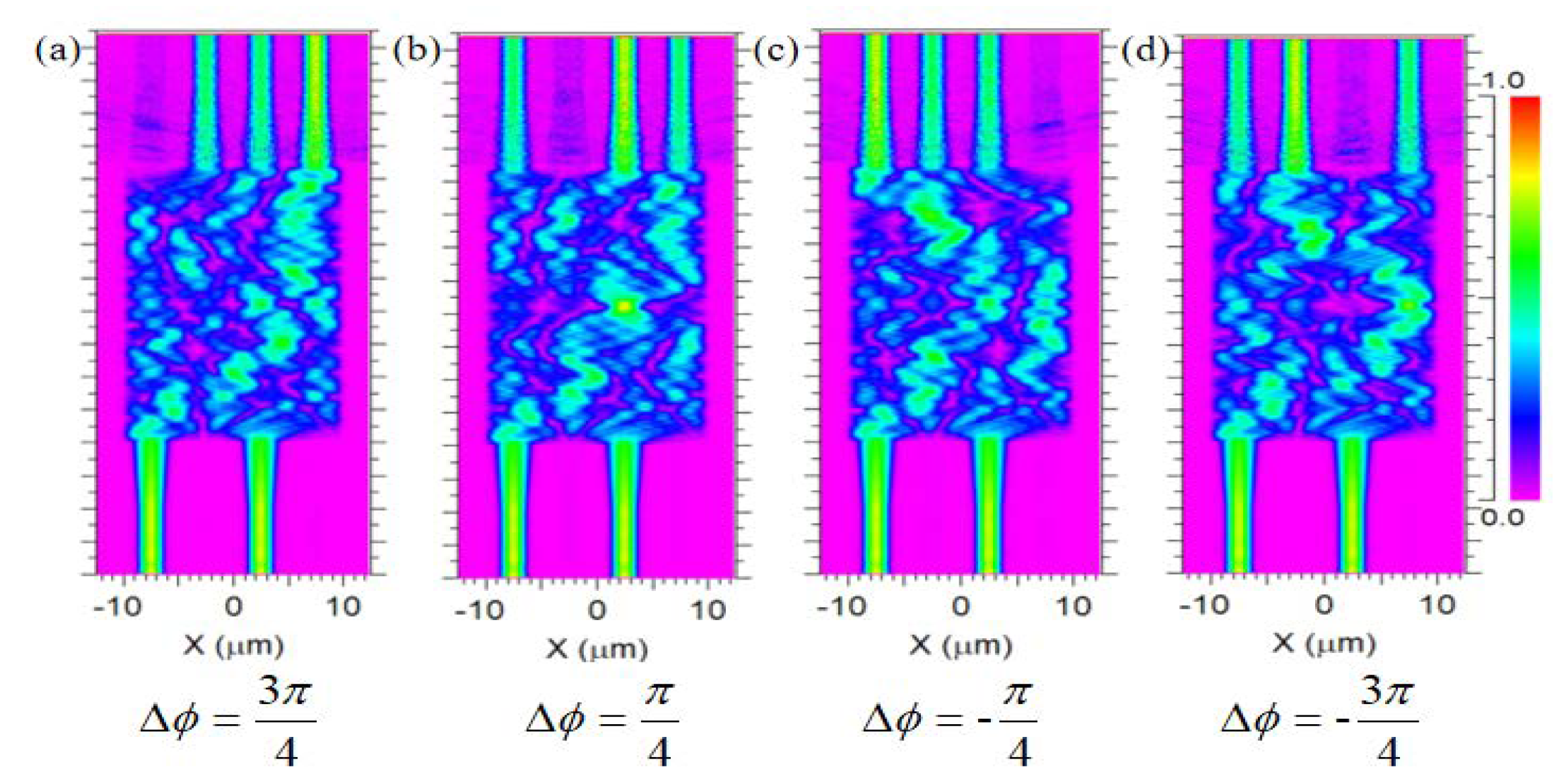
Input ports 1 and 3 carry a modulated optical signal with polarized phase information and an amplified local oscillator without modulation, respectively. The two beams interfere with each other in the multimode waveguide, and the relative phases of the output channels are 0°, 90°, −90°, and 180°, respectively. The output 1 and 4 channels are subtracted to obtain the in-phase component of the QPSK signal, which is called the I-channel. The output 2 and 3 channels are subtracted to obtain the quadrature component of QPSK signal, which is called the Q-channel. If signal light and local oscillation light are input simultaneously, the two sources of light will interfere with each other, and the output power of the four output channels will oscillate with the phase difference between the two input light beams. The field distributions and the relationships are shown in
Figure 2. By integrating two pairs of balanced photodetectors with the output ports 1,4 and 2,3, the photo-generated currents are detected, and the corresponding phase information can be demodulated.
According to the self-imaging principle, the light beam will generate multimode light fields in the multimode interference region [
18].
is defined as the beat length between the two lowest-order modes, which can be expressed as
where
and
are the propagation constants of the fundamental mode and the first-order mode, respectively,
is effective refractive index, and
is the working wavelength of the device. Here, we chose 1.55 μm. For the 4 × 4 MMI, the first length where four images appear is
where
is the effective width of the MMI, considering the lateral penetration depth of each mode field, which associates with the Goos–Hähnchen shifts at the ridge boundaries. For high-contrast waveguides, the penetration depth is very small; thus, the effective width is
Based on Equations (1)–(3), the width and length of the 4 × 4 MMI can be calculated. The upper cladding and the substrate are InP materials, while the refractive index is 3.17. The core layer of the deep-ridge waveguide is InGaAsP (1.05 Q), while the refractive index is 3.25. The thicknesses of the upper cladding and core layer are 1.5 μm and 0.5 μm, respectively. In this work, the width of the single-mode waveguide is 2.6 μm. That is, when the ridge width is equal to 2.6 μm, the mode refractive indices of TE and TM are equal, and the hybrid can achieve polarization insensitivity. The mode refractive index of the single-mode waveguide, , is calculated by a commercial software called fimmwave. The hybrid consists of a multimode waveguide with a width of 20 μm and a length of 842 μm, four input single-mode waveguides (channels 1 and 3 are useful channels) and four output single-mode waveguides with a width of 2.6 μm and a length of 200 μm. In order to reduce the loss and phase error caused by mode mismatch between the single-mode waveguide and the multimode waveguide, a tapered waveguide is introduced, the width of which changes from 2.6 μm to 3.7 μm. The subsequent simulation and fabrication are all based on the structure parameters introduced above.
3. Simulation and Manufacturing Tolerance Analysis
The three-dimensional beam propagation method (3D BPM) of the commercial software called R-soft is used to simulate and calculate the field distribution of the hybrid. The 3D BPM, which is based on the finite-difference beam propagation method (FD-BPM), is suitable for unidirectional transmission waveguides with large cross-section [
19]. In this research work, the refractive index and thickness of the core layer, as well as the width and length of the multimode waveguide, were simulated and analyzed to better understand the influence of these parameters on performances of the hybrid over the whole C-band.
The performance of an optical 90° hybrid is often quantified in terms of the common-mode rejection ratio (CMRR) and phase error (PE) [
12,
13]. The former CMRR is defined as
and
, where
are the power at each output channel 1, 2, 3, 4, which indicates the imbalance of I and Q channel. PE is the offset from standard deviation of the four output channels 1, 2, 3, 4, which is 0°, 90°, −90°, and 180°, respectively. It directly reflects the complexity on demodulation of the phase information in the input signal light.
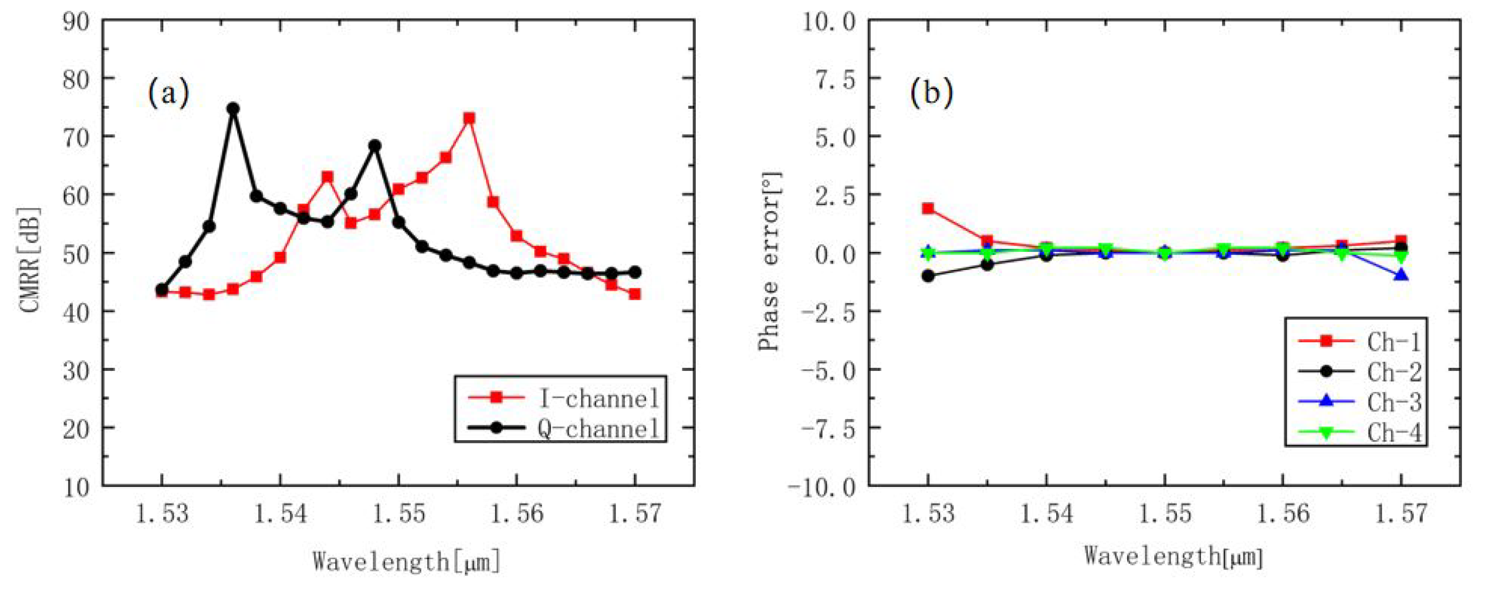
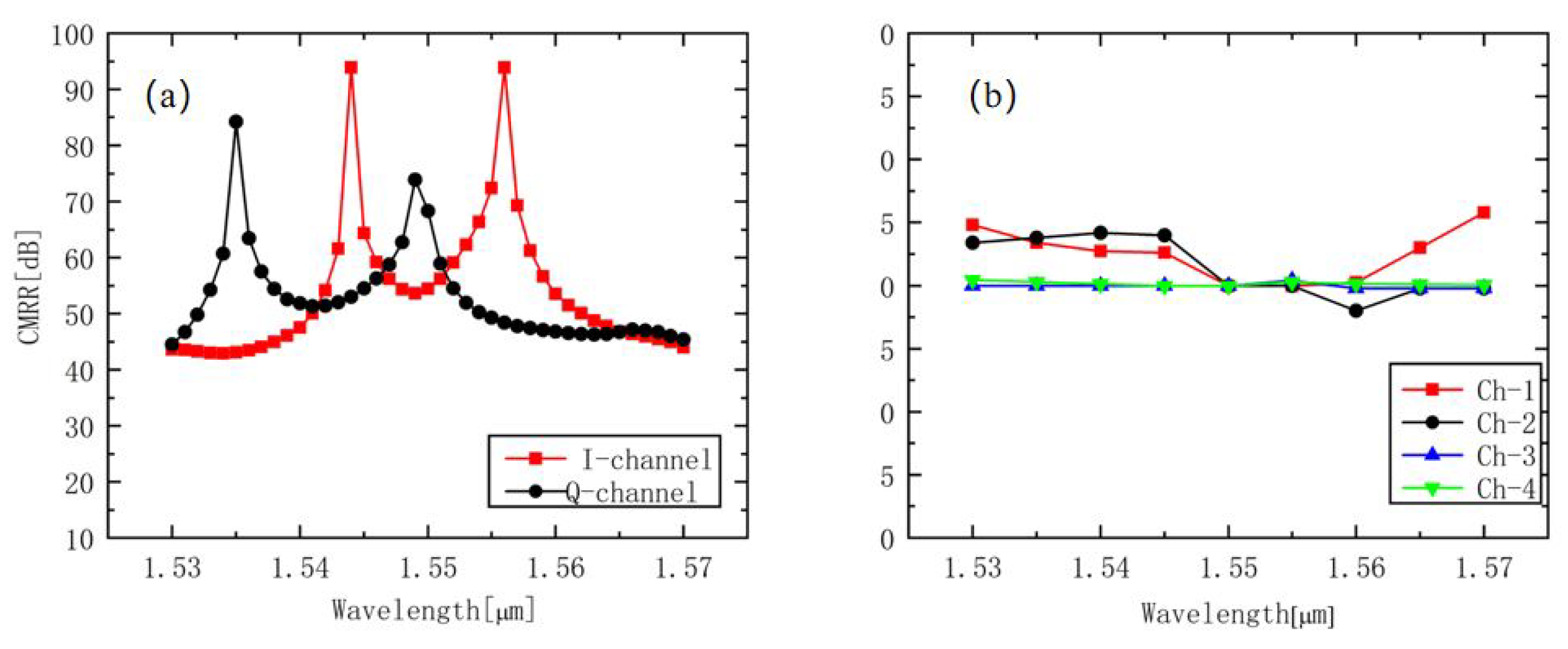
In our laboratory, InP and InGaAsP are grown on the InP substrate by metalorganic chemical vapor deposition (MOCVD). The thickness and refractive index of growing materials can be strictly controlled. In this part, the worst conditions in which the refractive index and thickness of the core layer are reduced by 0.01 and 0.1 μm are simulated and analyzed. As shown in
Figure 3, when the refractive index is reduced by 0.01, the simulated CMRRs are always above 40 dB and PEs are always below 2.5°. The hybrid is insensitive to the refractive index of the core layer. As shown in
Figure 4, when the thickness of the core layer is reduced by 0.1 μm, the simulated CMRRs are always above 40 dB and PEs are always below 5°. These results completely satisfy the optical internetworking forum (OIF) standard which is the international standard for optical 90° hybrids. Thus, we can get a conclusion that the error of material growth by MOCVD can be neglected.
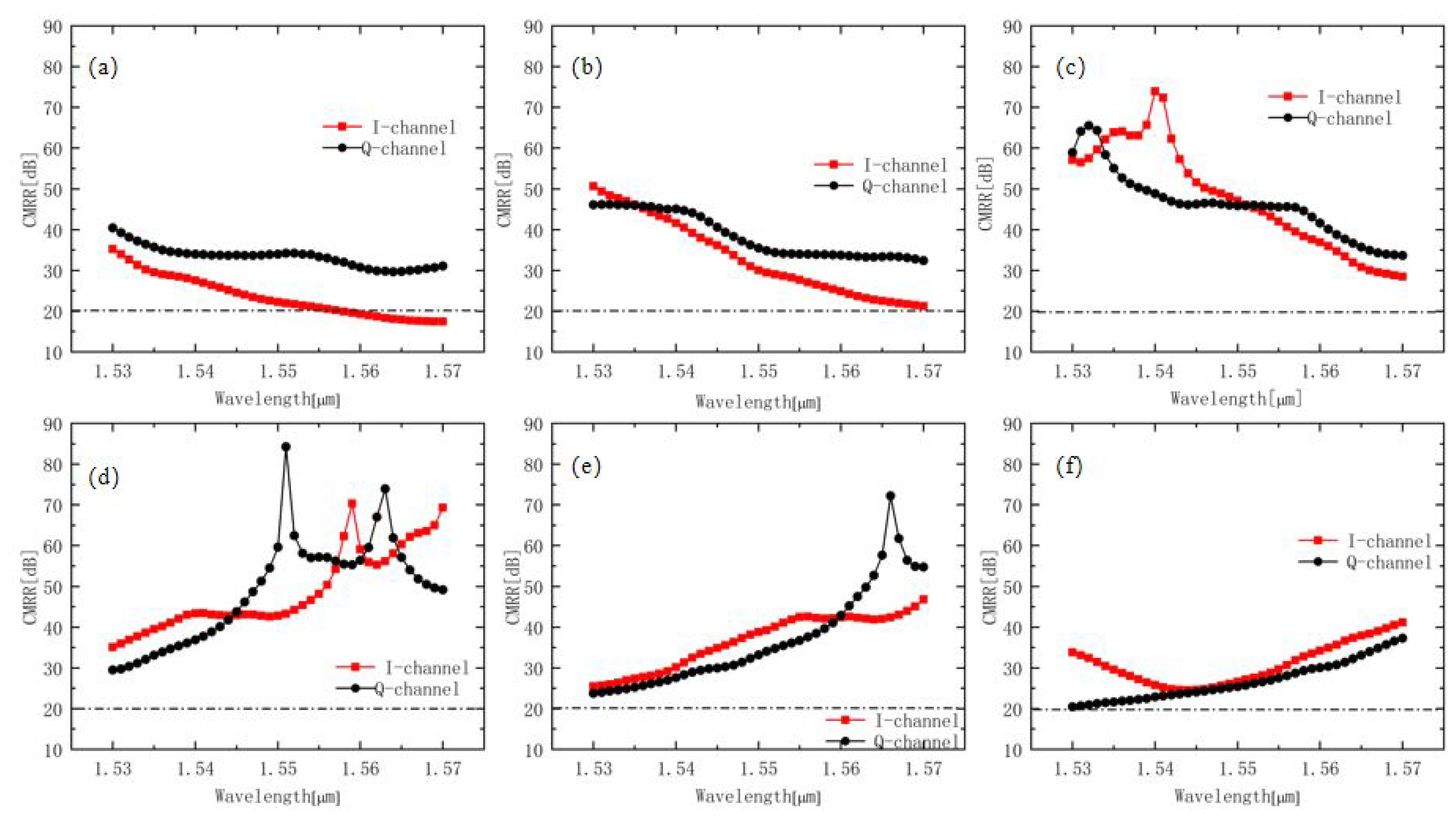
In the process of graphic transfer, lithography often directly determines the actual size of the device. The actual size of the fabricated hybrid is determined by the photolithography process, which can be easily affected by the quality of photoresist, exposure conditions, and environmental conditions. Under normal conditions, the size deviation of the fabricated devices is about 1 μm. Because the MMI is sensitive to width, the changes in CMRRs and PE were simulated and analyzed on the C-band when the width fluctuated from 0.1 μm to 0.3 μm.
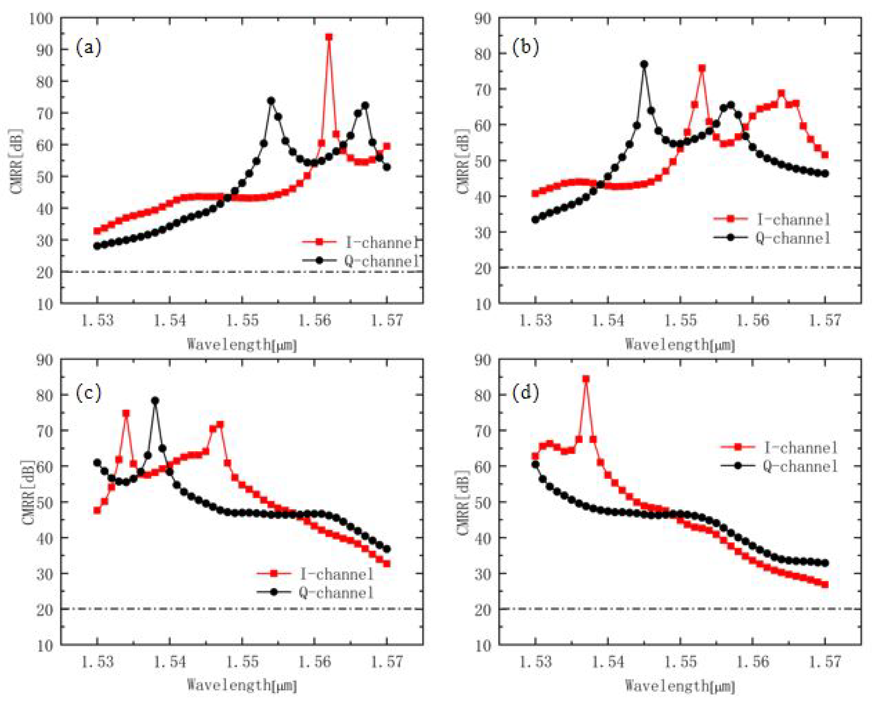
Figure 5 and
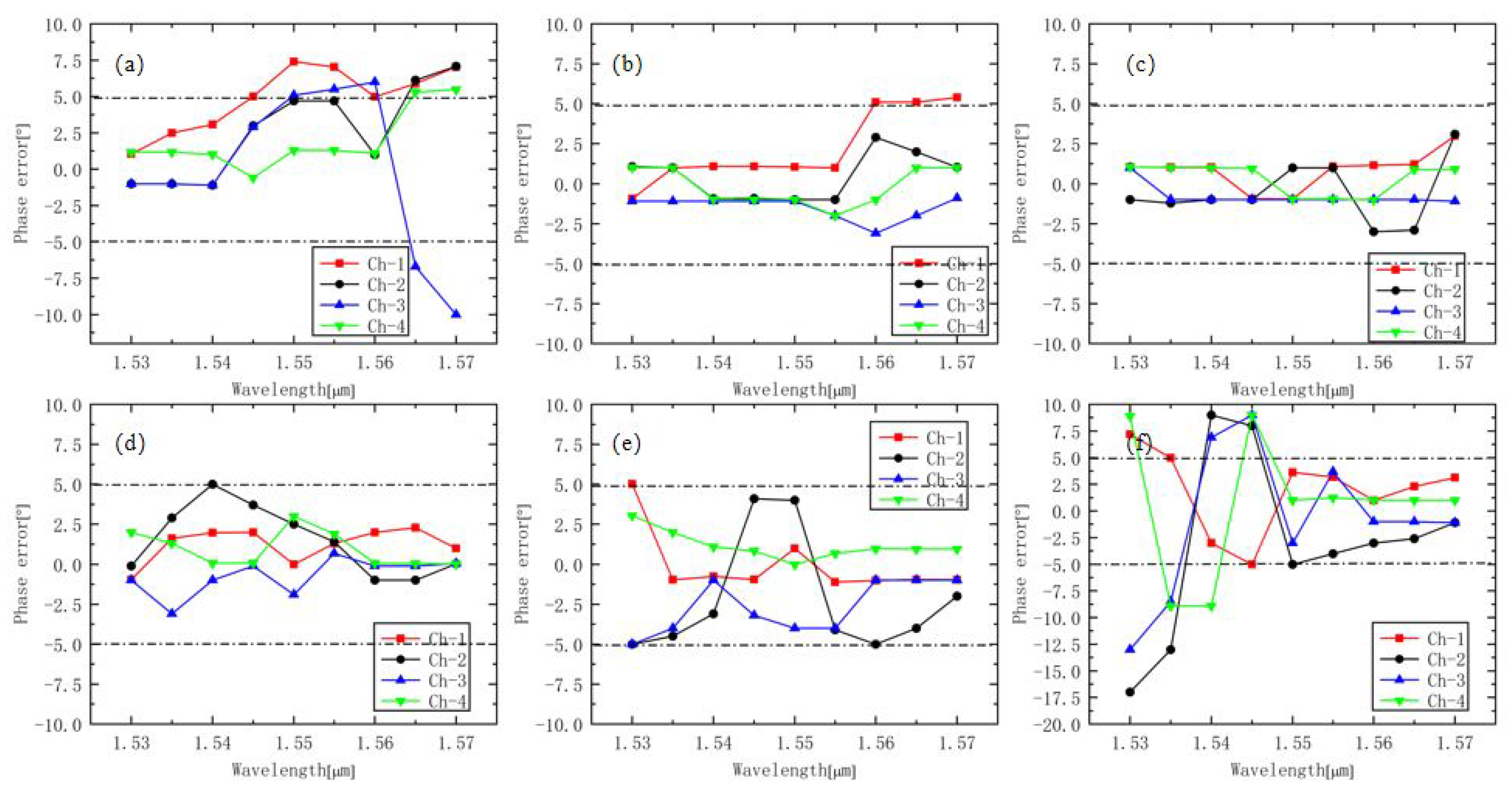
Figure 6 show the influences of different multimode waveguide widths on the CMRRs and PE. The widths were 19.7 μm, 19.8 μm, 19.9 μm, 20.1 μm, 20.2 μm, and 20.3 μm, respectively. Due to the deviation of the width, the field distribution in the multimode interference region changed, and the optimal interference length changed with the square rule. As shown in
Figure 5, when the width of hybrid increased from 19.7 μm to 20.3 μm, the CMRRs on the C-band basically remained above 20 dB, and they showed a trend of increasing before decreasing, even exceeding 30 dB closer to 20 μm. When the width increased from 19.7 μm to 19.9 μm, the CMRRs over the whole C-band decreased with the increase in wavelength, and the opposite result could be found from 20.1 μm to 20.3 μm. When close to 20 μm, the rate of rise or fall increased. The maximum value of CMMRs varied with the width of the MMI. In other words, the fabricated devices which deviate from the design value may continue to work at other wavelengths. In summary, we can conclude that there is little influence on CMRRs with width changes within 0.3 μm.
However, another key parameter, PE, was more sensitive to the width. When the width increased from 19.7 μm to 20.3 μm, the PE decreased before increasing. From 19.8 μm to 20.2 μm, the PE was less than 5° over the whole C-band, which indicates that the hybrid had the properties of a low error code rate. However, at 19.7 μm and 20.3 μm, the PE could only be kept within 5° on partial bands. When the width was 19.7 μm, the PE was less than 5° in the wavelength range of 1.53 μm to 1.545 μm, and only parts of the channels from 1.545 μm to 1.56 μm were less than 5°. The PE reached 10° at 1.57 μm but only 1.2° at 1.53 μm. On the contrary, when the width was 20.3 μm, the PE was less than 5° in the wavelength range of 1.55 μm to 1.57 μm, and only parts of the channels were less than 5° in the wavelength range of 1.535 μm to 1.55 μm. From 1.53 μm to 1.535 μm, the PE increased exponentially and reached 17.5° at 1.530 μm but only 2.5° at 1.57 μm. In terms of PE, only a 0.2-μm tolerance of device width could be applied to the whole C-band. This is because, with the change in hybrid width, the center wavelength corresponding to the tolerable phase error seriously shifted. The band corresponding to the hybrid with the width of 19.7 μm and 20.3 μm was not completely on the C-band. However, on the band with wavelength less than 1.53 μm or exceeding 1.57 μm, the PE at 19.7 μm or 20.3 μm could be within 5°.
In addition, we simulated the changes in CMRR and PE on the C-band when the length of the interference region fluctuated from 5 μm to 10 μm (in the simulation, the corresponding length of the hybrid with a width of 20 μm was 842 μm). As shown in
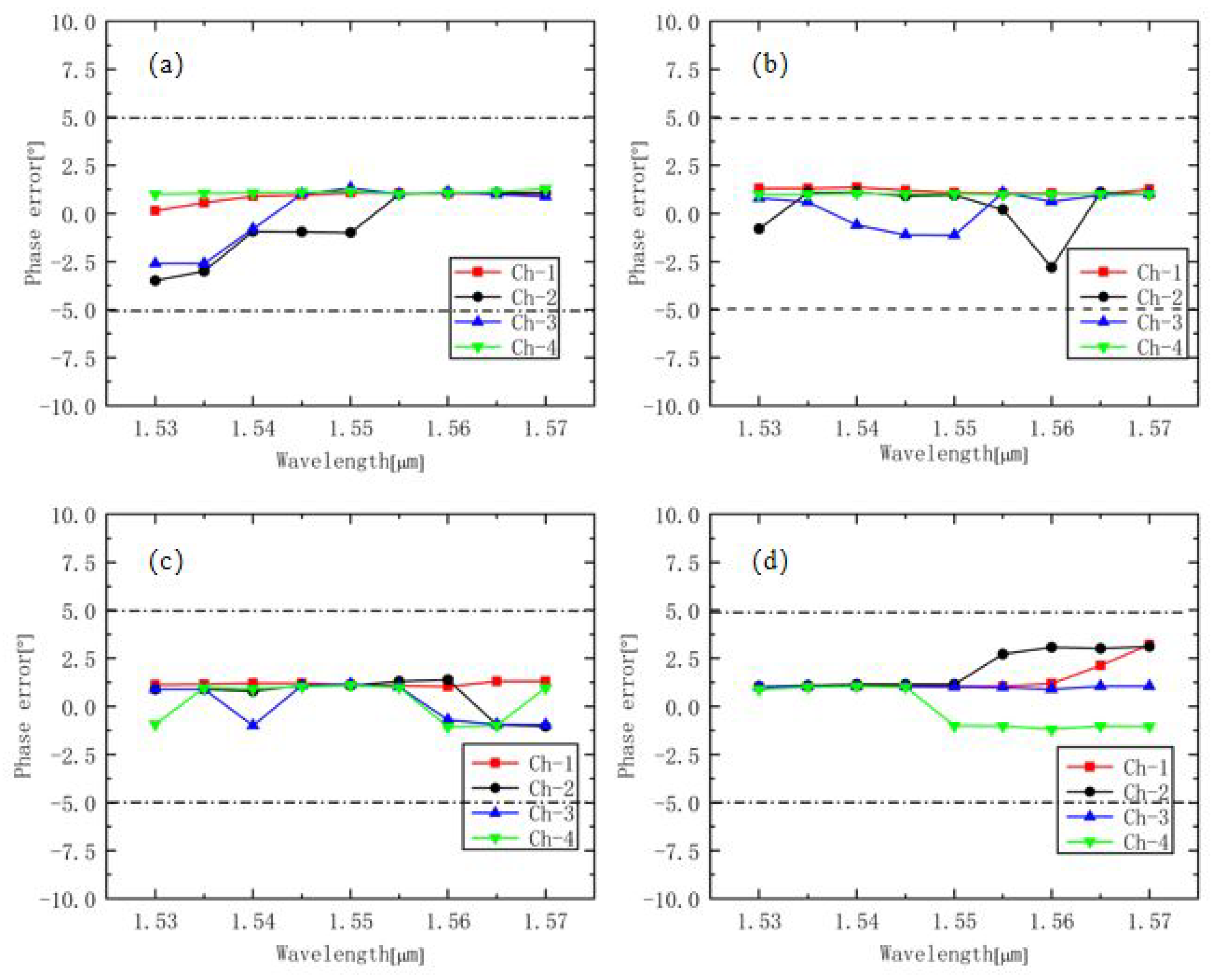
Figure 7 and
Figure 8, the interference lengths were 832 μm, 837 μm, 847 μm, and 852 μm. On the whole C-band, high CMRRs remained above 30 dB, and a small PE remained within 2.5°. The interference length with a range of 10 μm had no effect on the performance of the device. Therefore, in this process, we could adjust the interference length to reduce the influence of width variation on device performance.
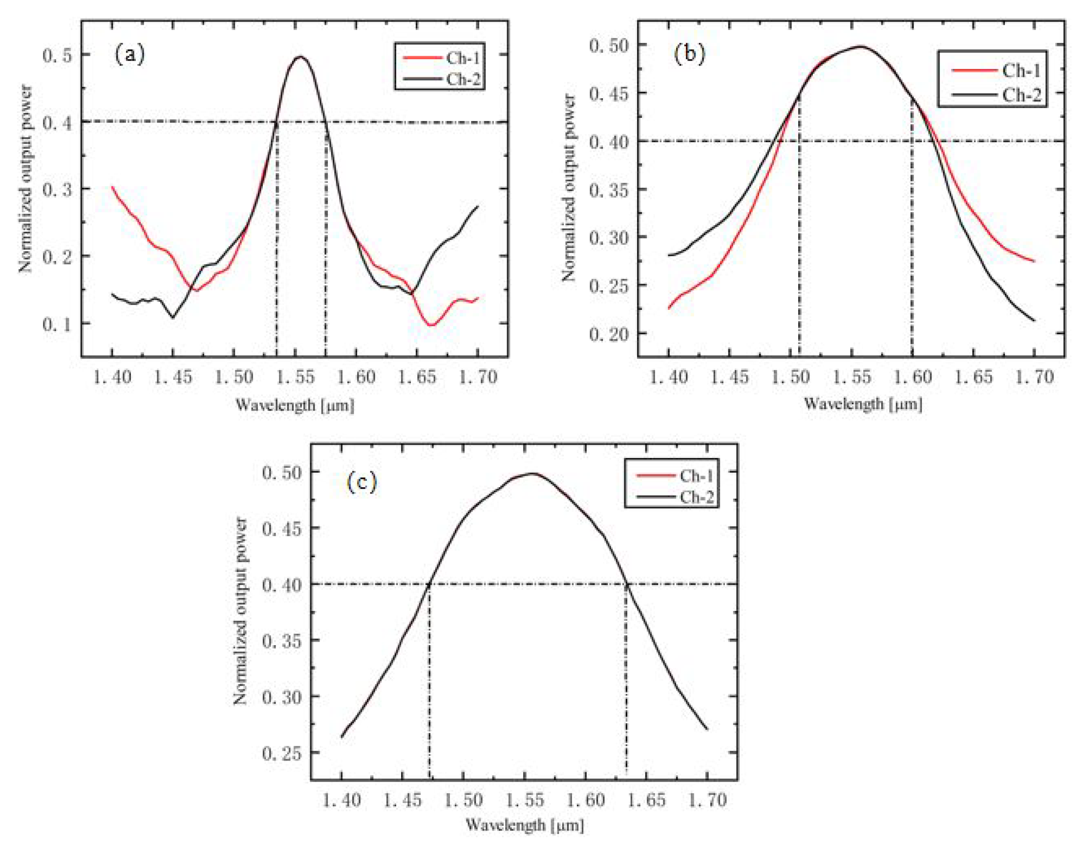
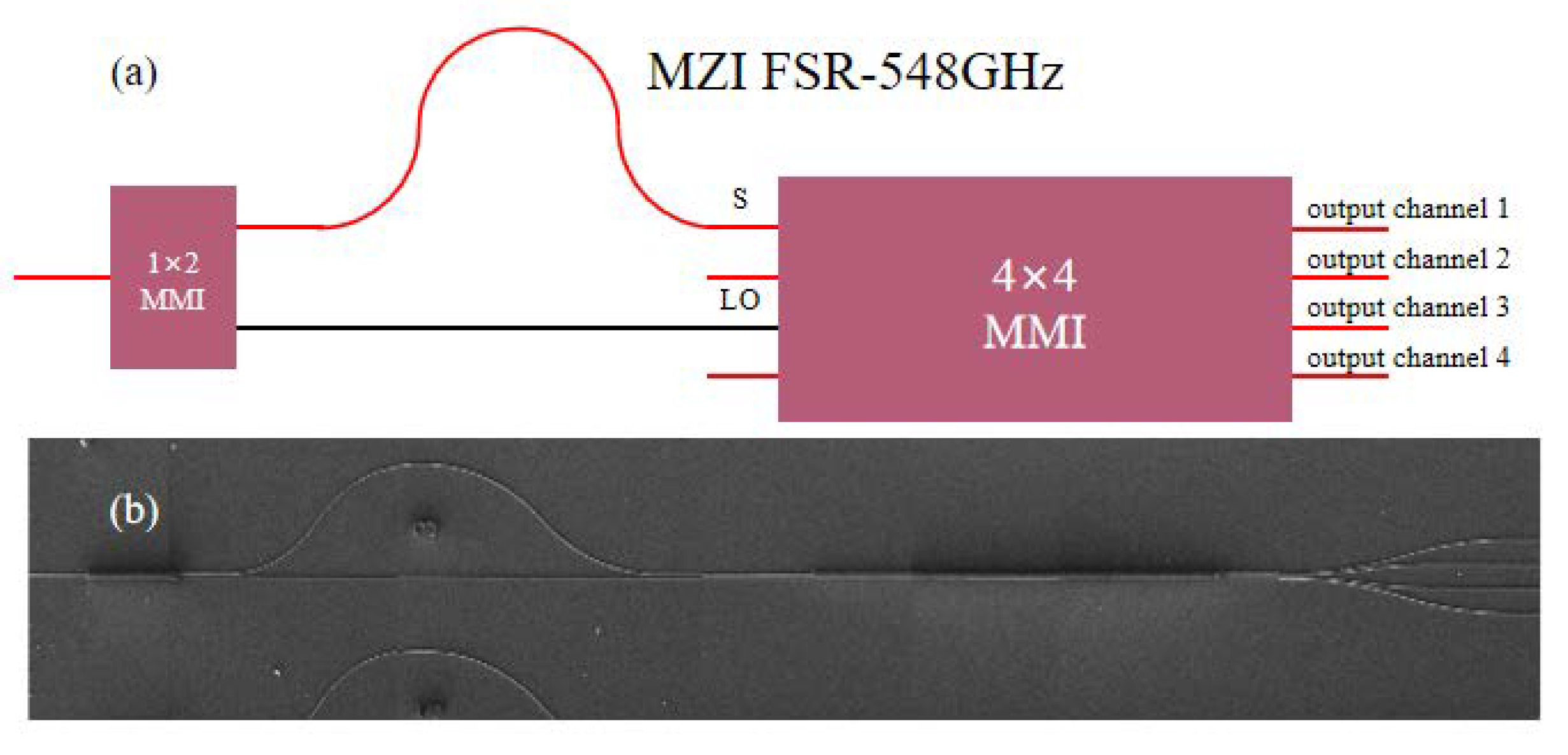
The normalized output power of three different types of 1 × 2 beam splitters on the C-band was simulated to compare the bandwidth.
Figure 9a–c shows the normalized output power of a 1 × 2 beam splitter with general, paired, and symmetrical interference on the C-band, respectively. In our devices, the 1 × 2 beam splitter was used as a 3-dB power divider; thus, we chose an output power of 0.4 to 0.5 as a valid output. The simulation results showed that the beam splitter with symmetrical interference, which had a maximum bandwidth of 160 nm from 1.47 μm to 1.63 μm, was the best choice. Therefore, the symmetrical interference beam splitter could guarantee high-power uniform beam splitting when detecting the band beyond the C-band.
5. Measurements and Result Analysis
The test bench set-up for testing the fabricated 90° hybrid is shown in
Figure 11. Polarization-maintaining fibers (PMFs) were used for device connecting and chip coupling. The wavelength of the tunable laser was tuned from 1530 nm to 1565 nm. The polarization of the beam was controlled in TE mode via a polarization controller (PC). The fused tapering fiber and the device were aligned precisely by means of a six-dimensional coupling system. A coupling efficiency of about 20% was obtained experimentally. The output signal was separated into two beams by using a beam splitter (BS). One beam was incident on the optical power meter to optimize the coupling efficiency, and the other one went into the optical spectrometer to measure the spectral response of the fabricated 90° hybrid.
The key parameters including PE and CMRRs were tested for the hybrid with a delay line and without delay line [
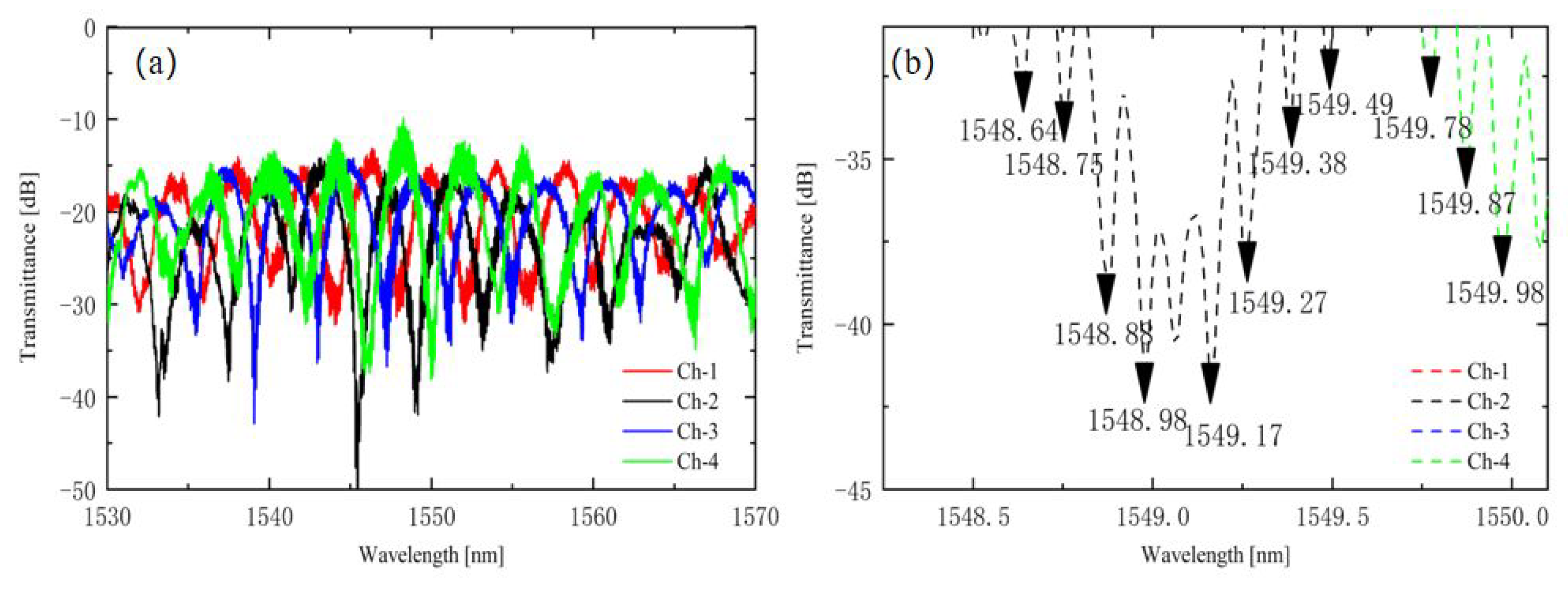
20]. By using a delay line, the phase difference between the two input beams can be adjusted by the wavelength. The measured transmission spectrum of the fabricated 90° hybrid is shown in
Figure 12a, and a partial amplification is shown in
Figure 12b. Among the four output channels, an orthogonal phase relationship was observed. A periodic weak oscillation in the measured spectrum was observed in
Figure 12b. Back reflection was the most probable reason. This kind of weak oscillation may affect the accuracy of the tested PE.
In this work, the location where weak oscillation occurred was calculated and analyzed. Suppose the cavity length between the two reflective surfaces is
L. According to the theory of cavity resonance, the frequency period of noise oscillation in the cavity can be obtained as follows:
where
is the frequency period of noise oscillation, and
n is the refractive index of the waveguide. Combined with
, the relationship between wavelength period and cavity length can be expressed as
where
m/s,
f =
Hz, and the measured wavelength interval
≈ 0.1 nm, as shown in
Figure 12b. If the refractive index
, then the cavity length
L ≈ 3.6 × 10
−3 m = 3.6 mm. The cavity length is exactly equal to the length of the delay line we designed. It can be concluded that periodic weak oscillation occurred between the two ends of the delay line, which is in good agreement with the theoretical calculation. Some scattering impurities or defects in the processing may have caused this phenomenon.
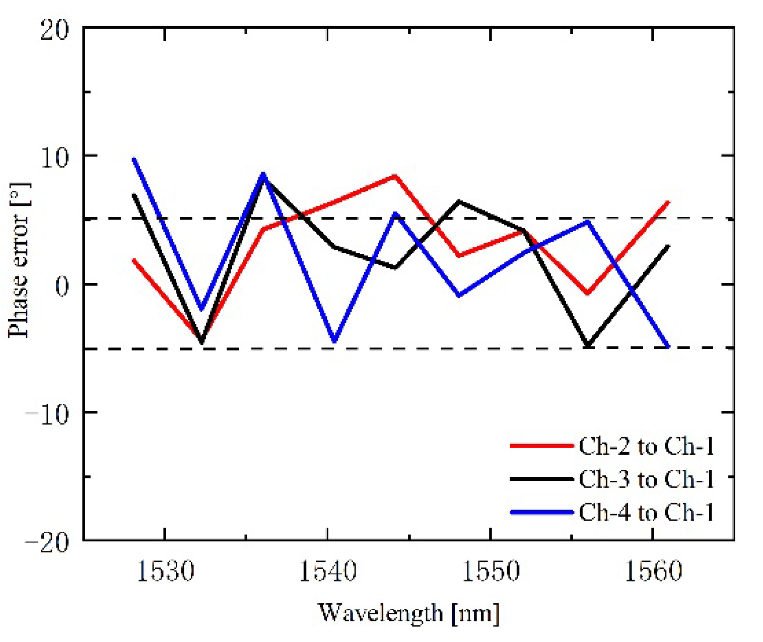
The PE can be calculated from the wavelength shift of the measured spectral response.
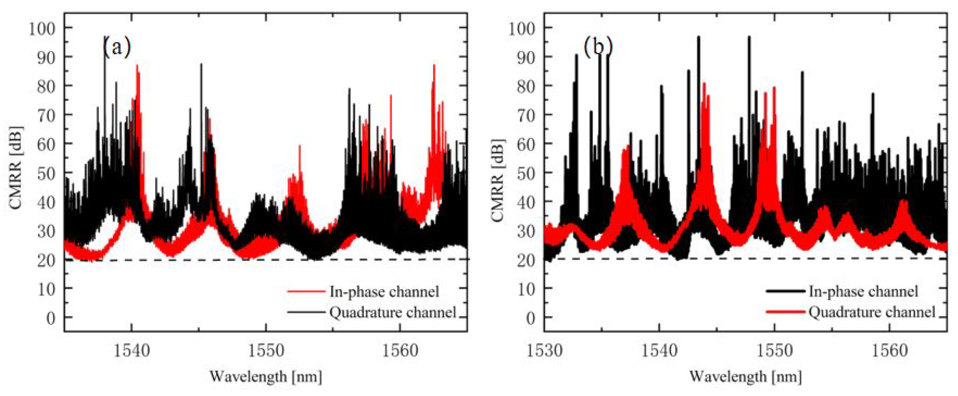
Figure 13 shows the calculated relative PE of the fabricated 90° hybrid, which was less than 5° in a range from 1545 nm to 1560 nm and less than 7° on the whole C-band. The measured results are close to the theoretical calculation. The CMRRs of the I/Q channel were measured from input ports 1 or 3, which is shown in
Figure 14. The CMRRs of the fabricated 90° hybrid were better than 25 dB on the whole C-band, which allows its use in a coherent receiver.

