Article

Tuning Plasmon Induced Reflectance with Hybrid Metasurfaces †

1
Photonics Laboratory, Tampere University, 33720 Tampere, Finland
2
Department of Electronic Engineering, Balochistan University of Information Technology, Engineering and Management Sciences, Quetta 87300, Pakistan
3
Nanotechnology Research Center, Bilkent University, 06800 Ankara, Turkey
*
Author to whom correspondence should be addressed.
This paper is an extended version of Habib, M.; Ozbay, E.; Caglayan, H. Tunable Reflection Type Plasmon Induced Transparency with Graphene. In Proceedings of the 2018 12th International Congress on Artificial Materials for Novel Wave Phenomena (Metamaterials), Espoo, Finland, 27 August–1 September 2018.
Photonics 2019, 6(1), 29; https://doi.org/10.3390/photonics6010029
Submission received: 14 February 2019 / Revised: 12 March 2019 / Accepted: 14 March 2019 / Published: 16 March 2019

Abstract

:
Electrically tunable metasurfaces with graphene offer design flexibility to efficiently manipulate and control light. These metasurfaces can be used to generate plasmon-induced reflectance (PIR), which can be tuned by electrostatic doping of the graphene layer. We numerically investigated two designs for tunable PIR devices using the finite difference time-domain (FDTD) method. The first design is based on two rectangular antennas of the same size and a disk; in the second design, two parallel rectangular antennas with different dimensions are used. The PIR-effect was achieved by weak hybridization of two bright modes in both devices and tuned by changing the Fermi level of graphene. A total shift of ∼362 nm was observed in the design with the modulation depth of 53% and a spectral contrast ratio of 76%. These tunable PIR devices can be used for tunable enhanced biosensing and switchable systems.

1. Introduction

Electromagnetically induced transparency (EIT) is a quantum interference phenomenon taking place between two laser excitation pathways [1,2]. The outcome of the EIT-effect is a transparent window within the absorption curve of a medium [3,4]. This effect is suitable for slow light applications [5], biosensing [6,7], optical storage [8], optical switching [9], and future quantum information processing devices [10]. Recently, the possibility of merging plasmonics and metamaterials has led to the achievement of analogues of the EIT system, and is known as plasmon-induced transparency (PIT). The PIT effect has been observed in different structures, such as hybrid metal-graphene metasurfaces [11,12,13,14,15], integrated photonics [16], metallic nanoparticles [17,18], wave-guide systems [19,20], and plasmonic coupled cavities [21,22]. The metasurfaces [23,24,25,26,27,28] can be tuned electrically [29,30,31,32,33,34,35,36], thermally [37], and mechanically [38].
The size and shape of these structures provide different resonances depending on the coupling of the modes with the incident light. The bright modes are radiative and spectrally broadened due to the direct coupling of incident light. On the other hand, the dark modes—which do-not couple directly to light—can be weakly damped and spectrally narrow. The PIT effect can be realized by the weak hybridization/detuning of two bright modes [39,40] or by the destructive interference of dark–bright modes [13]. Recently, the hybrid designs have been used to obtain a tunable PIT response [12,41,42,43,44]. These designs are based on a graphene layer at the bottom of metasurfaces which tunes the PIT effect at different Fermi levels (Ef). However, these designs are limited to operation in specific wavelength ranges due to the limitations of transparent substrates [14,15,40].
An alternative to PIT called plasmon-induced reflectance (PIR) was initially proposed by Ding et al. [45]. This design is based on a cut wire serving as a dark mode and a split ring resonator serving as a bright mode to achieve PIR. Recently, Lie et al. suggested the use of graphene to obtain electrically tunable devices, as the field localization for the graphene layer is increased four-fold on top of the reflecting surface [46]. The tunable PIR response can be used for better detection and modulation with enhanced localized electric field due to the reflecting surface at the bottom [47,48,49,50].
Graphene is first ever discovered 2-D material, with a honeycomb lattice of carbon atoms. Graphene has remarkable optical properties that can be tuned by electrostatic doping. The optical response of graphene is explained by the Pauli blocking principle [51], as graphene forms a conical band diagram. There are two kinds of band transition in graphene, depending on the incident photon energy. If the energy is less than 2Ef, intra-band transition is pronounced; if the energy is higher than 2Ef, inter-band transition is pronounced. The Ef of graphene is explained as:
E f = ν F π n ,
where is the reduced Planck’s constant, n is the charge density, and νF is the Fermi velocity. The Ef of graphene can be controlled by changing the charge density on the graphene layer.
The surface conductivity of graphene is modeled by considering it as an isotropic infinitely thin layer that is conductive from both sides. The intra-band and inter-band transitions are presented by the following equations, respectively [52]:
σ i n t r a = j e 2 k B T π 2 ( ω 2 j Γ ) μ c k B T + 2 l n e μ c k B T + 1 ,
σ i n t e r = j e 2 4 π l n 2 | μ c | ( ω 2 j Γ ) 2 | μ c | + ( ω 2 j Γ ) ,
where kB is the Boltzmann constant and e is the electron charge (a constant). However, T (temperature), Γ (scattering rate), μ c (chemical potential), and ωc (angular frequency) are the parameters that can be changed based on the conditions and graphene properties.
Overall, graphene provides the possibility to miniaturize optical devices down to atom-layer thickness. It has the advantage of tuning the Ef by applying the gate voltage, and it has a wide optical response range from terahertz to optical frequencies [53]. These properties make graphene the best candidate for long-range electrically tunable materials [54].
In this work, we present two different designs to obtain PIR. In the first one, we used two rectangular plasmonic gold (Au) antennas with an Au disk at the center. Both rectangular antennas served as a single bright mode and the disk served as a second bright mode, and we achieved PIR by the coupling/detuning of these modes. In the second device, we used only two rectangular Au antennas with different lengths, both serving as the bright modes. The PIR response of devices was tuned by changing the Ef of graphene at the bottom.

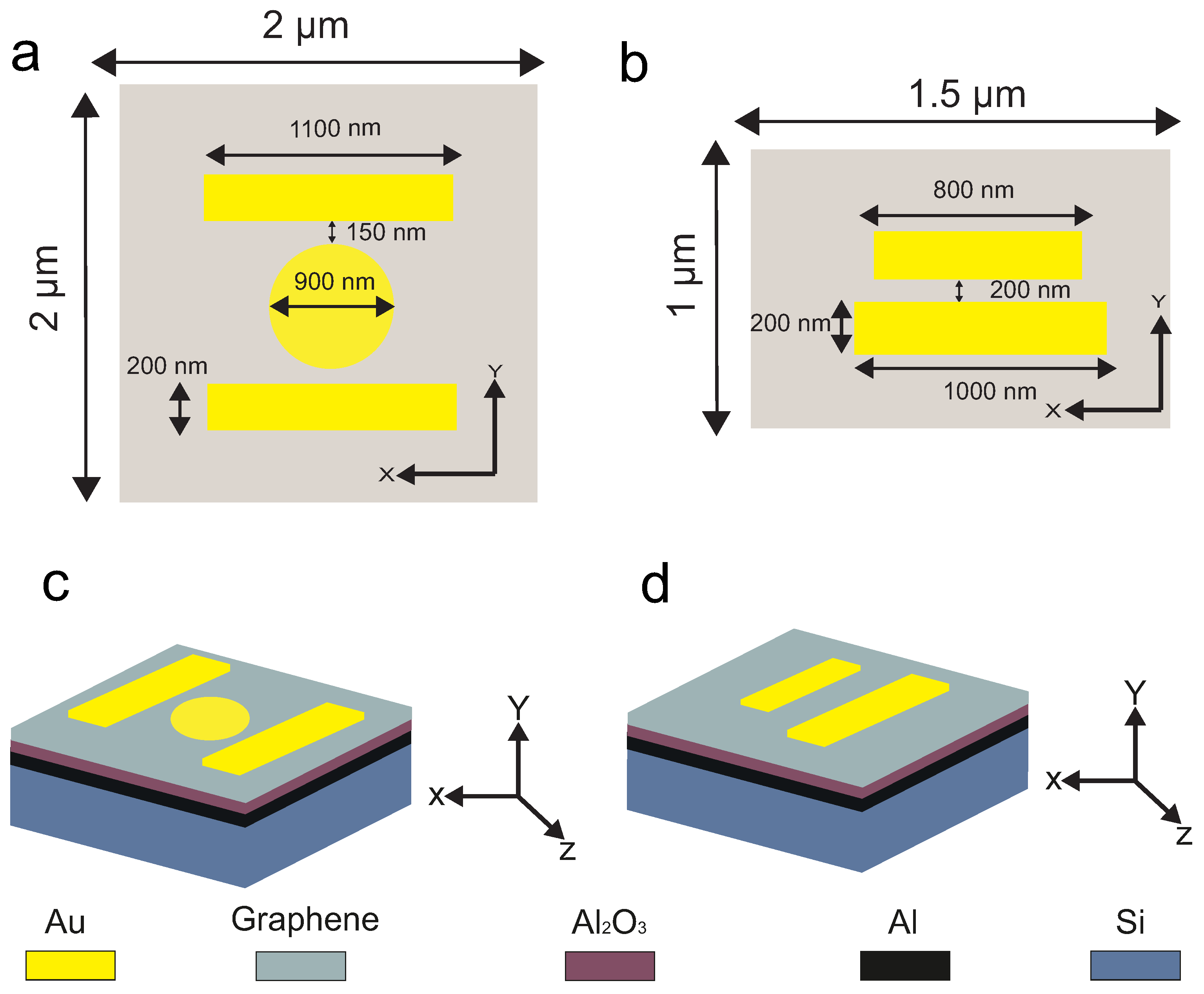
2. Numerical Investigation

We numerically investigated both devices using the finite difference time domain (FDTD) method. We used commercially available Lumerical FDTD Solutions. The unit cell of the first device was composed of two rectangles and a disk at the center. The disk had a diameter (D) = 900 nm, both rectangular antennas had the length (L) = 1100 nm, width (W) = 200 nm, and the thickness of all structures Was kept at 50 nm. The rectangular antennas were placed 150 nm away from the edge of the disk. The unit cell was periodic in x and y axes, with a periodicity of 2 μ m. The perfect matched layer (PML) boundary condition was applied in the direction of propagation (i.e., z axis). The unit cell and 3D schematic of this device are presented in Figure 1a,c, respectively. The devices were illuminated by a plane wave propagating along the z axis direction, with electric field component (E) parallel to the x axis.
For the simulations, silicon (Si) was used as a substrate with 100 nm of aluminum (Al) as a reflecting surface and 50 nm of aluminum oxide (Al2O3) as an insulator layer. The graphene layer was introduced as a dispersive 2-D material between the oxide layer and 50-nm-thick Au PIR structures. The Γ of graphene was set as 2.4 × 10¹² s 1 , which is complementary to experimental works [12], T was set as 300 K, and μ c was varied from 0.2 to 0.8 eV.
The reflection spectrum of the device is presented in Figure 2. The disk showed a strong response and produced resonance at a shorter wavelength (3.62 μ m), as shown in the inset of Figure 2a (pink color). Similarly, the two rectangular antennas also had a strong response at a longer wavelength (4.39 μ m), shown in the inset of Figure 2a (green color). There Was no PIR response when the structure itself was excited individually. However, when we brought them to an optimum distance of 150 nm, the PIR response was produced by the detuning of the two resonances (3.94 μ m). This PIR response could be controlled by the size and shape of the structures. In this study, in order to tune the PIR response, the Ef of the graphene layer was increased from 0.2 to 0.8 eV. The simulation results for 0.2 eV (black), 0.5 eV (blue), and 0.8 eV (red) are presented in Figure 3a. As the Ef of graphene increased, a blue shift was observed in the PIR response of the device.
For the second device, we used two parallel rectangular Au antennas with two different lengths (L1) = 1.0 μ m and (L2) = 0.8 μ m. The width of the antennas was 200 nm and they were separated by 200 nm (D). The periodicity of the device was 1.5 μ m along the x axis and 1 μ m along the y axis. The unit cell and 3D schematic of the second device are presented in Figure 1b,d, respectively.
The simulation results of the second device were quite similar to our first design, with a slight shift in the PIR-effect due to the smaller dimensions. Both antennas had their own resonances at 3.49 μ m and 4.22 μ m for shorter and longer wavelength, respectively, as shown in the inset of Figure 2b. The PIR response was achieved by detuning these bright modes at 3.80 μ m, as presented in Figure 2b.
The E-field results for the resonance wavelengths of 3.62 μ m and 4.39 μ m are shown in Figure 3a,c, respectively. Moreover, the E-field magnitude for reflection peak at 3.94 μ m is presented in Figure 3b. These results show that the disk and rectangular antennas were individually excited at their resonance wavelengths and acted as the bright modes. However, at 3.94 μ m both structures were excited simultaneously to produce the PIR-effect.
The E-field results for the second device showed that the shorter antenna was excited at 3.49 μ m and the longer one at 4.22 μ m, as shown in Figure 4a,c, respectively. On the other hand, at 3.80 μ m both of the rectangular antennas were simultaneously excited, resulting in the PIR-effect (Figure 4b).

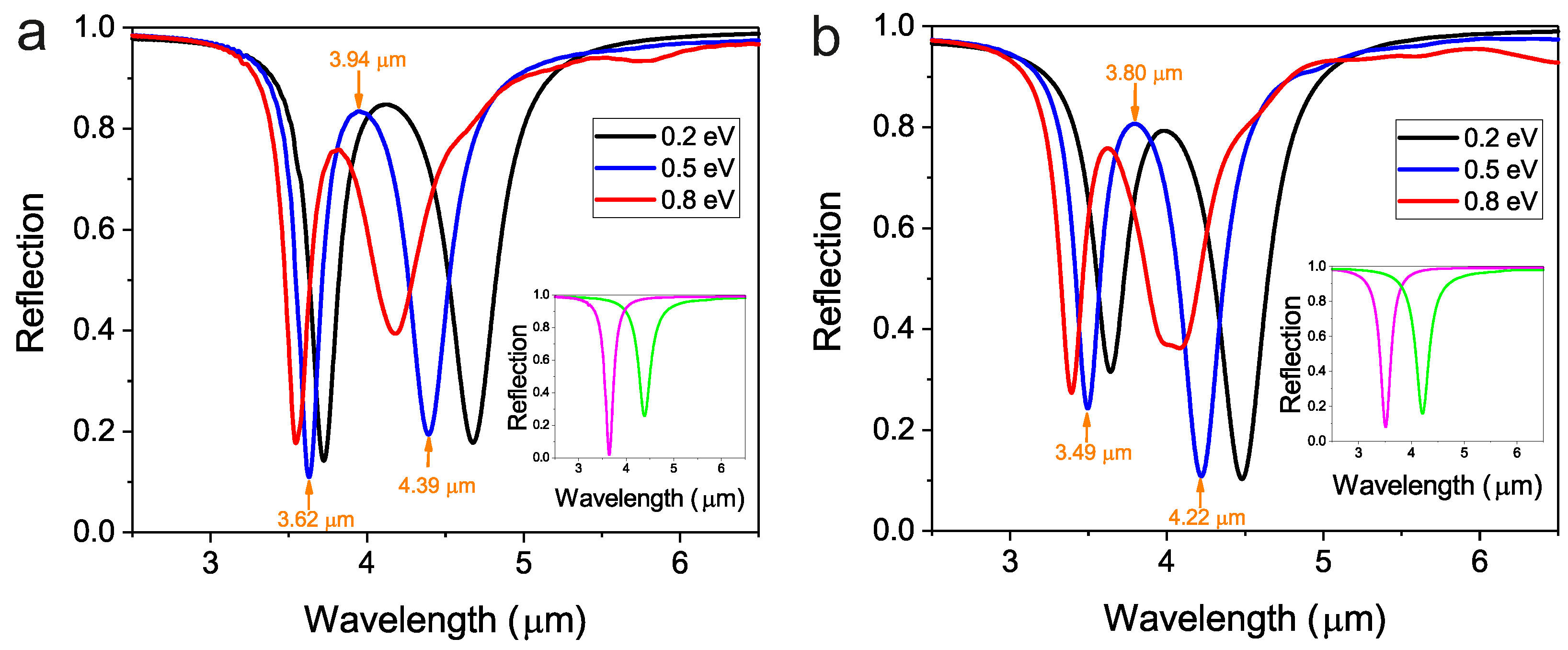
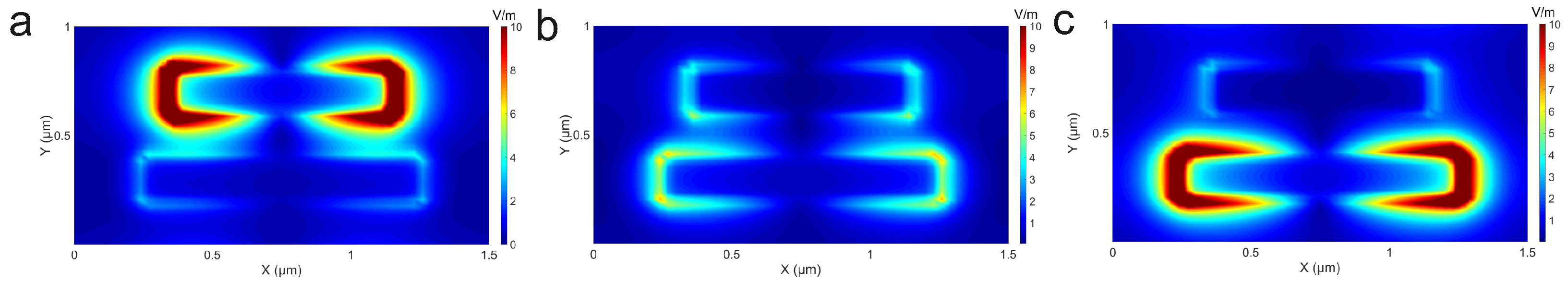
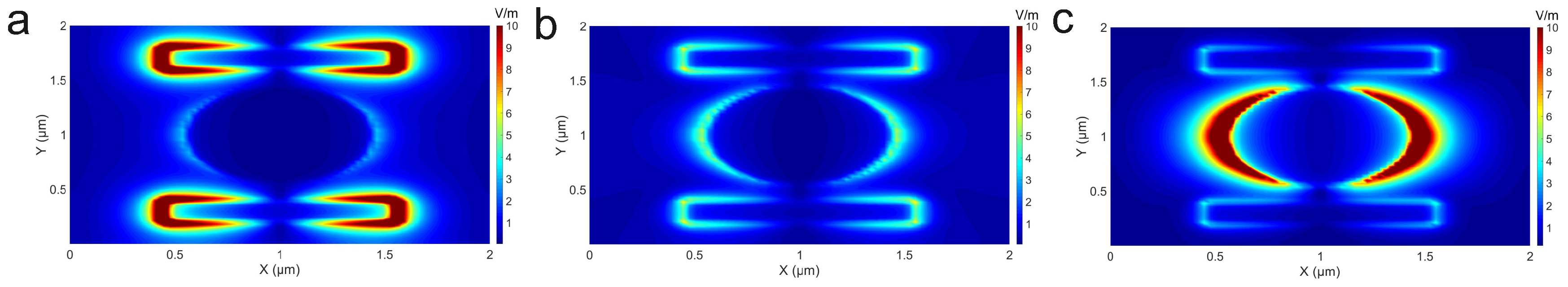
3. Experimental Investigation

The second device was fabricated as described in the Materials and Methods section. The scanning electron microscopy (SEM) of the fabricated sample is presented in the inset of Figure 5. The reflection measurements were done using a Fourier-transform infrared spectroscopy (FTIR) device integrated with a microscope. We used the microscope focus individual matrix of sample 200 × 200 μ m2.
The Ef of the graphene was tuned using top gating method, the gate voltage was changed from −0.6 V to 2.4 V, corresponding to the Ef of 0.5 and 0.8 eV, respectively—the details are explained in Reference [12]. A blue shift was observed in the PIR by changing the gate voltage from to 2.4 V (red) presented in Figure 5, and a red shift was observed by applying −0.6 V.

4. Discussion

For the first device, a total shift of 306.6 nm was observed by changing the Ef from 0.2 to 0.8 eV. Similarly, for the second device a total shift of 362.2 nm was observed by the numerical investigation. In the experiment, the total shift of 184.4 nm was observed for a 3 V change in the gate voltage. In order to quantitatively investigate the change in the intensity of reflection by changing the Ef of graphene, the modulation depth (Mdepth) was defined as
M d e p t h = ( R R g ) R × 100 ,
where R is the reflection at minimum Ef and Rg is the reflection at maximum Ef. The Mdepth of the first device was 50% and it was 53% for the second device.
The spectral contrast ratio (Scon) is used to evaluate the performance of the PIR response in optical applications, and is described as:
S c o n = ( R p e a k R d i p ) ( R p e a k + R d i p ) × 100 ,
where Rpeak is the intensity of the reflection peak and Rdip is the intensity of the resonance dip. The Scon of our first device was 76.7% and 76.3% for the second device. Moreover, a good agreement of simulation and experimental results was observed for the second device, providing proof of the concept. The electrically tunable devices can be used for tunable sensing and switching application.

5. Materials and Methods

The device was fabricated on top of Si substrate, a 100-nm Al layer was deposited using electron-beam evaporation, and a 50 nm smooth layer of oxide was deposited using atomic layer deposition (ALD) technique for better lithography. Commercially available chemical vapor deposition (CVD)-grown graphene on Copper (Cu) was transferred on top of the oxide layer by etching the bottom side graphene and Cu. Later, the sample was coated with poly (methyl methacrylate) (PMMA) resist and a conductive polymer by spin-coating and baking. The sample was exposed to electron beam lithography and developed using methyl isobutyl ketone (MIBK):isopropyl alcohol(IPA) in a 1:1 ratio. The developed sample was coated with 5 nm of titanium (Ti) for better adhesion and 50 nm of Au. The sample was left inside the acetone for 24 h for the lift-off process. The SEM image of the device is presented in the inset of Figure 5.
The top gating method was used to apply the gate voltage to graphene. The second substrate (BaF2) was fabricated using photo-lithography to make the metal contacts at the corners and transparent window at the center for optical measurements. This substrate with metal contacts was placed on top of the PIR device and separated by an insulating tape. An ionic liquid was inserted between the two substrates; a source was connected to the graphene layer and metal contacts using a conductive tape [33,34,55]. By applying the gate voltage, capacitance was produced between the graphene layer and the gold contact due to the presence of ionic liquid, and we could control the charge accumulation on top of the graphene layer. This control of charge accumulation was used to tune the Ef of the graphene layer.

6. Conclusions

Overall, the PIR was realized by simple designs of metasurfaces on top of a graphene layer. Furthermore, our hybrid metal-graphene structure could achieve an electrically tunable PIR-effect. The total shifts of 306 nm and 362 nm were observed in the first and second device by changing the Ef from 0.2 to 0.8 eV. Moreover, a total shift of ∼184 nm shift was observed experimentally by applying 3 V. These PIR designs with the Mdepth of 53% and Scon of 76% are suitable for effective optical modulation and switching applications.

Author Contributions

M.H. did simulations, fabrication and characterization. M.H., E.O. and H.C. contributed to the concept and writing of the paper.

Funding

Competitive funding to strengthen university research profiles was funded by the Academy of Finland, Decision No. 301820.

Acknowledgments

One of the authors (E.O.) also acknowledges the partial support from the Turkish Academy of Sciences.

Conflicts of Interest

The funders had no role in the design of the study; in the collection, analyses, or interpretation of data; in the writing of the manuscript, or in the decision to publish the results.

References

  1. Boller, K.J.; Imamoğlu, A.; Harris, S.E. Observation of electromagnetically induced transparency. Phys. Rev. Lett. 1991, 66, 2593. [Google Scholar] [CrossRef] [PubMed]
  2. Marangos, J.P. Electromagnetically induced transparency. J. Mod. Opt. 1998, 45, 471–503. [Google Scholar] [CrossRef]
  3. Kasapi, A.; Jain, M.; Yin, G.; Harris, S.E. Electromagnetically induced transparency: Propagation dynamics. Phys. Rev. Lett. 1995, 74, 2447. [Google Scholar] [CrossRef]
  4. Harris, S.; Field, J.; Kasapi, A. Dispersive properties of electromagnetically induced transparency. Phys. Rev. A 1992, 46, R29. [Google Scholar] [CrossRef] [PubMed]
  5. Krauss, T.F. Why do we need slow light? Nat. Photonics 2008, 2, 448. [Google Scholar] [CrossRef]
  6. Vafapour, Z.; Hajati, Y.; Hajati, M.; Ghahraloud, H. Graphene-based mid-infrared biosensor. JOSA B 2017, 34, 2586–2592. [Google Scholar] [CrossRef]
  7. Vafapour, Z. Near infrared biosensor based on Classical Electromagnetically Induced Reflectance (Cl-EIR) in a planar complementary metamaterial. Opt. Commun. 2017, 387, 1–11. [Google Scholar] [CrossRef]
  8. Novikova, I.; Walsworth, R.L.; Xiao, Y. Electromagnetically induced transparency-based slow and stored light in warm atoms. Laser Photonics Rev. 2012, 6, 333–353. [Google Scholar] [CrossRef]
  9. Chen, J.; Wang, P.; Chen, C.; Lu, Y.; Ming, H.; Zhan, Q. Plasmonic EIT-like switching in bright-dark-bright plasmon resonators. Opt. Express 2011, 19, 5970–5978. [Google Scholar] [CrossRef] [PubMed]
  10. Fleischhauer, M.; Imamoglu, A.; Marangos, J.P. Electromagnetically induced transparency: Optics in coherent media. Rev. Mod. Phys. 2005, 77, 633. [Google Scholar] [CrossRef]
  11. Amin, M.; Farhat, M.; Baǧcı, H. A dynamically reconfigurable Fano metamaterial through graphene tuning for switching and sensing applications. Sci. Rep. 2013, 3, 2105. [Google Scholar] [CrossRef]
  12. Habib, M.; Rashed, A.R.; Ozbay, E.; Caglayan, H. Graphene-based tunable plasmon induced transparency in gold strips. Opt. Mater. Express 2018, 8, 1069–1074. [Google Scholar] [CrossRef]
  13. Liu, N.; Langguth, L.; Weiss, T.; Kästel, J.; Fleischhauer, M.; Pfau, T.; Giessen, H. Plasmonic analogue of electromagnetically induced transparency at the Drude damping limit. Nat. Mater. 2009, 8, 758. [Google Scholar] [CrossRef]
  14. Zhu, Y.; Hu, X.; Fu, Y.; Yang, H.; Gong, Q. Ultralow-power and ultrafast all-optical tunable plasmon-induced transparency in metamaterials at optical communication range. Sci. Rep. 2013, 3, 2338. [Google Scholar] [CrossRef]
  15. Hokmabadi, M.P.; Philip, E.; Rivera, E.; Kung, P.; Kim, S.M. Plasmon-induced transparency by hybridizing concentric-twisted double split ring resonators. Sci. Rep. 2015, 5, 15735. [Google Scholar] [CrossRef]
  16. Vlasov, Y.A.; O’boyle, M.; Hamann, H.F.; McNab, S.J. Active control of slow light on a chip with photonic crystal waveguides. Nature 2005, 438, 65. [Google Scholar] [CrossRef]
  17. Rohde, C.; Hasegawa, K.; Deutsch, M. Plasmon-assisted transparency in metal-dielectric microspheres. Opt. Lett. 2007, 32, 415–417. [Google Scholar] [CrossRef] [PubMed]
  18. Yannopapas, V.; Paspalakis, E.; Vitanov, N.V. Electromagnetically induced transparency and slow light in an array of metallic nanoparticles. Phys. Rev. B 2009, 80, 035104. [Google Scholar] [CrossRef]
  19. Zhang, J.; Bai, W.; Cai, L.; Xu, Y.; Song, G.; Gan, Q. Observation of ultra-narrow band plasmon induced transparency based on large-area hybrid plasmon-waveguide systems. Appl. Phys. Lett. 2011, 99, 181120. [Google Scholar] [CrossRef]
  20. Zhang, Z.; Fan, Y.; Long, Y.; Yin, P. Theoretical realization of dynamically tunable double plasmonically induced transparency in a graphene-based waveguide structure. Opt. Mater. 2017, 72, 632–636. [Google Scholar] [CrossRef]
  21. Xu, J.; Fan, Y.; Yang, R.; Fu, Q.; Zhang, F. Realization of switchable EIT metamaterial by exploiting fluidity of liquid metal. Opt. Express 2019, 27, 2837–2843. [Google Scholar] [CrossRef] [PubMed]
  22. Zhu, Y.; Hu, X.; Yang, H.; Gong, Q. On-chip plasmon-induced transparency based on plasmonic coupled nanocavities. Sci. Rep. 2014, 4, 3752. [Google Scholar] [CrossRef] [PubMed]
  23. Fan, Y.; Shen, N.H.; Koschny, T.; Soukoulis, C.M. Tunable terahertz meta-surface with graphene cut-wires. Acs Photonics 2015, 2, 151–156. [Google Scholar] [CrossRef]
  24. Fan, Y.; Shen, N.H.; Zhang, F.; Zhao, Q.; Wei, Z.; Zhang, P.; Dong, J.; Fu, Q.; Li, H.; Soukoulis, C.M. Photoexcited graphene metasurfaces: Significantly enhanced and tunable magnetic resonances. ACS Photonics 2018, 5, 1612–1618. [Google Scholar] [CrossRef]
  25. Tao, H.; Padilla, W.J.; Zhang, X.; Averitt, R.D. Recent progress in electromagnetic metamaterial devices for terahertz applications. IEEE J. Sel. Top. Quantum Electron. 2011, 17, 92–101. [Google Scholar] [CrossRef]
  26. Pendry, J.B.; Schurig, D.; Smith, D.R. Controlling electromagnetic fields. Science 2006, 312, 1780–1782. [Google Scholar] [CrossRef] [PubMed]
  27. Ozbay, E. Plasmonics: Merging photonics and electronics at nanoscale dimensions. Science 2006, 311, 189–193. [Google Scholar] [CrossRef] [PubMed]
  28. Balci, O.; Kakenov, N.; Karademir, E.; Balci, S.; Cakmakyapan, S.; Polat, E.O.; Caglayan, H.; Özbay, E.; Kocabas, C. Electrically switchable metadevices via graphene. Sci. Adv. 2018, 4, eaao1749. [Google Scholar] [CrossRef]
  29. Fan, Y.; Shen, N.H.; Zhang, F.; Wei, Z.; Li, H.; Zhao, Q.; Fu, Q.; Zhang, P.; Koschny, T.; Soukoulis, C.M. Electrically tunable Goos–Hänchen effect with graphene in the terahertz regime. Adv. Opt. Mater. 2016, 4, 1824–1828. [Google Scholar] [CrossRef]
  30. Fan, Y.; Qiao, T.; Zhang, F.; Fu, Q.; Dong, J.; Kong, B.; Li, H. An electromagnetic modulator based on electrically controllable metamaterial analogue to electromagnetically induced transparency. Sci. Rep. 2017, 7, 40441. [Google Scholar] [CrossRef]
  31. Kim, T.T.; Kim, H.D.; Zhao, R.; Oh, S.S.; Ha, T.; Chung, D.S.; Lee, Y.H.; Min, B.; Zhang, S. Electrically tunable slow light using graphene metamaterials. ACS Photonics 2018, 5, 1800–1807. [Google Scholar] [CrossRef]
  32. Cakmakyapan, S.; Caglayan, H.; Ozbay, E. Coupling enhancement of split ring resonators on graphene. Carbon 2014, 80, 351–355. [Google Scholar] [CrossRef]
  33. Ozdemir, O.; Aygar, A.M.; Balci, O.; Kocabas, C.; Caglayan, H.; Ozbay, E. Enhanced tunability of V-shaped plasmonic structures using ionic liquid gating and graphene. Carbon 2016, 108, 515–520. [Google Scholar] [CrossRef]
  34. Aygar, A.M.; Balci, O.; Cakmakyapan, S.; Kocabas, C.; Caglayan, H.; Ozbay, E. Comparison of back and top gating schemes with tunable graphene fractal metasurfaces. ACS Photonics 2016, 3, 2303–2307. [Google Scholar] [CrossRef]
  35. Goldflam, M.; Driscoll, T.; Chapler, B.; Khatib, O.; Marie Jokerst, N.; Palit, S.; Smith, D.; Kim, B.J.; Seo, G.; Kim, H.T.; et al. Reconfigurable gradient index using VO2 memory metamaterials. Appl. Phys. Lett. 2011, 99, 044103. [Google Scholar] [CrossRef]
  36. Urzhumov, Y.; Lee, J.S.; Tyler, T.; Dhar, S.; Nguyen, V.; Jokerst, N.M.; Schmalenberg, P.; Smith, D.R. Electronically reconfigurable metal-on-silicon metamaterial. Phys. Rev. B 2012, 86, 075112. [Google Scholar] [CrossRef]
  37. Zheludev, N.I.; Kivshar, Y.S. From metamaterials to metadevices. Nat. Mater. 2012, 11, 917. [Google Scholar] [CrossRef] [PubMed]
  38. Shin, D.; Urzhumov, Y.; Jung, Y.; Kang, G.; Baek, S.; Choi, M.; Park, H.; Kim, K.; Smith, D.R. Broadband electromagnetic cloaking with smart metamaterials. Nat. Commun. 2012, 3, 1213. [Google Scholar] [CrossRef] [PubMed]
  39. Stockman, M.I.; Faleev, S.V.; Bergman, D.J. Localization versus delocalization of surface plasmons in nanosystems: Can one state have both characteristics? Phys. Rev. Lett. 2001, 87, 167401. [Google Scholar] [CrossRef]
  40. Zhang, H.; Cao, Y.; Liu, Y.; Li, Y.; Zhang, Y. A novel graphene metamaterial design for tunable terahertz plasmon induced transparency by two bright mode coupling. Opt. Commun. 2017, 391, 9–15. [Google Scholar] [CrossRef]
  41. Habib, M.; Ozbay, E.; Caglayan, H. Tunable reflection type plasmon induced transparency with graphene. In Proceedings of the IEEE 12th International Congress on Artificial Materials for Novel Wave Phenomena (Metamaterials), Espoo, Finland, 27 August–1 September 2018; pp. 170–172. [Google Scholar]
  42. Xiao, F.; Zhu, W.; Shang, W.; Mei, T.; Premaratne, M.; Zhao, J. Electrical control of second harmonic generation in a graphene-based plasmonic Fano structure. Opt. Express 2015, 23, 3236–3244. [Google Scholar] [CrossRef] [PubMed]
  43. Liu, C.; Liu, P.; Yang, C.; Lin, Y.; Liu, H. Analogue of dual-controlled electromagnetically induced transparency based on graphene metamaterial. Carbon 2018, 142, 354–362. [Google Scholar] [CrossRef]
  44. He, X.; Yang, X.; Lu, G.; Yang, W.; Wu, F.; Yu, Z.; Jiang, J. Implementation of selective controlling electromagnetically induced transparency in terahertz graphene metamaterial. Carbon 2017, 123, 668–675. [Google Scholar] [CrossRef]
  45. Ding, C.-F.; Zhang, Y.-T.; Yao, J.-Q.; Sun, C.-L.; Xu, D.-G.; Zhang, G.-Z. Reflection-type electromagnetically induced transparency analogue in terahertz metamaterials. Chin. Phys. B 2014, 23, 124203. [Google Scholar] [CrossRef]
  46. Liu, Y.; Dai, Y.; Feng, Q.; Shan, Y.; Du, L.; Xia, Y.; Lu, G.; Liu, F.; Du, G.; Tian, C.; et al. Enhanced light-matter interactions in graphene-covered dielectric magnetic mirrors. Opt. Express 2017, 25, 30754–30763. [Google Scholar] [CrossRef]
  47. Gao, L.; Ren, W.; Liu, B.; Saito, R.; Wu, Z.S.; Li, S.; Jiang, C.; Li, F.; Cheng, H.M. Surface and interference coenhanced Raman scattering of graphene. ACS Nano 2009, 3, 933–939. [Google Scholar] [CrossRef]
  48. Fang, Z.; Liu, Z.; Wang, Y.; Ajayan, P.M.; Nordlander, P.; Halas, N.J. Graphene-antenna sandwich photodetector. Nano Lett. 2012, 12, 3808–3813. [Google Scholar] [CrossRef]
  49. Xia, F.; Mueller, T.; Lin, Y.m.; Valdes-Garcia, A.; Avouris, P. Ultrafast graphene photodetector. Nat. Nanotechnol. 2009, 4, 839. [Google Scholar] [CrossRef]
  50. Furchi, M.; Urich, A.; Pospischil, A.; Lilley, G.; Unterrainer, K.; Detz, H.; Klang, P.; Andrews, A.M.; Schrenk, W.; Strasser, G.; et al. Microcavity-integrated graphene photodetector. Nano Lett. 2012, 12, 2773–2777. [Google Scholar] [CrossRef]
  51. Mak, K.F.; Ju, L.; Wang, F.; Heinz, T.F. Optical spectroscopy of graphene: From the far infrared to the ultraviolet. Solid State Commun. 2012, 152, 1341–1349. [Google Scholar] [CrossRef]
  52. Hanson, G.W. Dyadic Green’s functions and guided surface waves for a surface conductivity model of graphene. J. Appl. Phys. 2008, 103, 064302. [Google Scholar] [CrossRef]
  53. Zhu, W.; Xiao, F.; Kang, M.; Sikdar, D.; Premaratne, M. Tunable terahertz left-handed metamaterial based on multi-layer graphene-dielectric composite. Appl. Phys. Lett. 2014, 104, 051902. [Google Scholar] [CrossRef]
  54. Wang, F.; Zhang, Y.; Tian, C.; Girit, C.; Zettl, A.; Crommie, M.; Shen, Y.R. Gate-variable optical transitions in graphene. Science 2008, 320, 206–209. [Google Scholar] [CrossRef] [PubMed]
  55. Habib, M.; Gokbayrak, M.; Ozbay, E.; Caglayan, H. Electrically controllable plasmon induced reflectance in hybrid metamaterials. Appl. Phys. Lett. 2018, 113, 221105. [Google Scholar] [CrossRef]
Figure 1. The unit cell of (a) the first device with two rectangular antennas and a disk. (b) The second device with two parallel rectangular antennas. (c,d) 3D schematics of the first and second devices, respectively.
Photonics 06 00029 g001
Figure 2. Simulated reflection results of (a) the first device and (b) the second device at 0.2, 0.5, and 0.8 eV . The insets show the reflection spectra of the bright modes excited individually: (a) shorter rectangular antenna (pink), longer antenna (green), and (b) rectangular antennas (pink) and disk (green).
Photonics 06 00029 g002
Figure 3. Electric-field (E-field) magnitudes at 0.5 eV: (a) E-field magnitude at 3.62 μ m. (b) E-field magnitude at 3.94 μ m. (c) E-field magnitude at 4.39 μ m.
Photonics 06 00029 g003
Figure 4. E-field magnitudes at 0.5 eV: (a) E-field magnitude at 3.49 μ m. (b) E-field magnitude at 3.80 μ m. (c) E-field magnitude at 4.22 μ m.
Photonics 06 00029 g004
Figure 5. Reflection results of the two rectangular antenna design. The SEM image is presented in the inset.
Photonics 06 00029 g005

