Article

Design an All-Optical Combinational Logic Circuits Based on Nano-Ring Insulator-Metal-Insulator Plasmonic Waveguides

by
Saif Hasan Abdulnabi
and
Mohammed Nadhim Abbas
*
Department of Electrical Engineering, College of Engineering, University of Baghdad, Baghdad 10001, Iraq
*
Author to whom correspondence should be addressed.
Photonics 2019, 6(1), 30; https://doi.org/10.3390/photonics6010030
Submission received: 17 February 2019 / Revised: 14 March 2019 / Accepted: 15 March 2019 / Published: 19 March 2019

Abstract

:
In this paper, we propose, analyze and simulate a new configuration to simulate all-optical combinational logic functions based on Nano-rings insulator-metal-insulator (IMI) plasmonic waveguides. We used Finite Element Method (FEM) to analyze the proposed plasmonic combinational logic functions. The analyzed combinational logic functions are Half-Adder, Full-Adder, Half-Subtractor, and Comparator One-Bit. The operation principle of these combinational logic functions is based on the constructive and destructive interferences between the input signal(s) and control signal. Numerical simulations show that a transmission threshold exists (0.25) which allows all proposed four plasmonic combinational logic functions to be achieved in one structure. As a result, the transmission threshold value measures the performance of the proposed plasmonic combinational logic functions. We use the same structure with the same dimensions at 1550 nm wavelength for all proposed plasmonic combinational logic functions. The proposed all-optical combinational logic functions structure contributes significantly to photonic integrated circuits construction and all-optical signal processing nano-circuits.

1. Introduction

All-optical devices based on Surface Plasmon Polaritons (SPP) are the topic of comprehensive research in recent years. All-optical SPP devices motivate extensively new research to overcome the major performance constraints of semiconductor electronic devices which suffer from inherent delay and high heat generation, as well as to overcome the problem of photonics devices, that is, the diffraction limit. Therefore, the utilization of the aforementioned devices enables the manipulation of light on a subwavelength scale [1]. However, the main idea is to control the constructive/destructive interference of two or more light signals in two or more plasmonic waveguides [2,3]. The constructive/destructive interferences are considered as a switch operation and the devices that perform this operation called all-optical switching devices [4]. Plasmonic logic gates such as OR, AND, NOR, NAND, XOR, XNOR and NOT logical operations can make the basic units of future subwavelength processors [2]. Recently, many all-optical plasmonic structures have provided nanoscale logic gates [5,6,7,8,9].
On the other hand, many all-optical structures provided combinational logic functions [10,11,12,13,14,15,16,17,18,19]. Some of these works [10,11,12,13,14,15] investigate a surface plasmon polariton (SPP) to achieve a desired function(s) from the combinational logic functions, each combinational logic circuit has their own way to realize the function of the combinational logic circuit, such as a different number of combinational logic functions, different types of combinational logic functions, etc. For examples, a nanoscale plasmonic half-adder architecture as a simple plasmonic processor has been introduced and verified based on interference of SPP modes in Reference [10], an optical half-adder has been realized with a footprint of only 10 μm × 28 μm in Reference [11], a plasmonic adder-subtractor module based on a Metal-Insulator-Metal (MIM) ring resonator is proposed in Reference [12], a compact design of a one-bit magnitude comparator using a nonlinear plasmonic Mach–Zehnder Interferometer (MZI) has been designed in Reference [13], and a low-power ultra-compact chip-integrated all-optical logic half-adder and full-adder in X-shaped plasmonic microstructures covered with a nonlinear nanocomposite layer, and etched in plasmonic integrated circuits directly experimentally realized in Reference [14]. According to our knowledge, so far, there is no theoretical or experimental demonstration of a combinational logic functions structure that satisfies the requirements of ultra-small feature size, and four plasmonic combinational logic functions in one structure.
In this article, we offer the sub-micron size structure, enhancing the transmission (exceeding 100%), and the largest number (four plasmonic combinational logic functions) of plasmonic combinational logic function in the same structure with the same of resonance frequency and the same transmission threshold in structure with Nano-rings resonator and plasmonic Nano-waveguides. The plasmonic combinational logic functions that are proposed, designed and simulated are half-adder, full-adder, half-subtractor, and comparator one-bit. The simulation results are obtained by FEM. In the future, these devices will be the gateway to the Nano-photonic integrated circuits applications.
The organization of this article is as follows: Section 2 contains the proposed structure layout and theoretical operation concept. In Section 3, the simulation results and performance of the proposed all-optical plasmonic combinational logic function are presented, demonstrated and discussed. In Section 4, a comparison between the proposed plasmonic combinational logic functions and previous researches is introduced. Finally, we conclude the suggested work in Section 5.

2. Structure Layout and Theoretical Concept

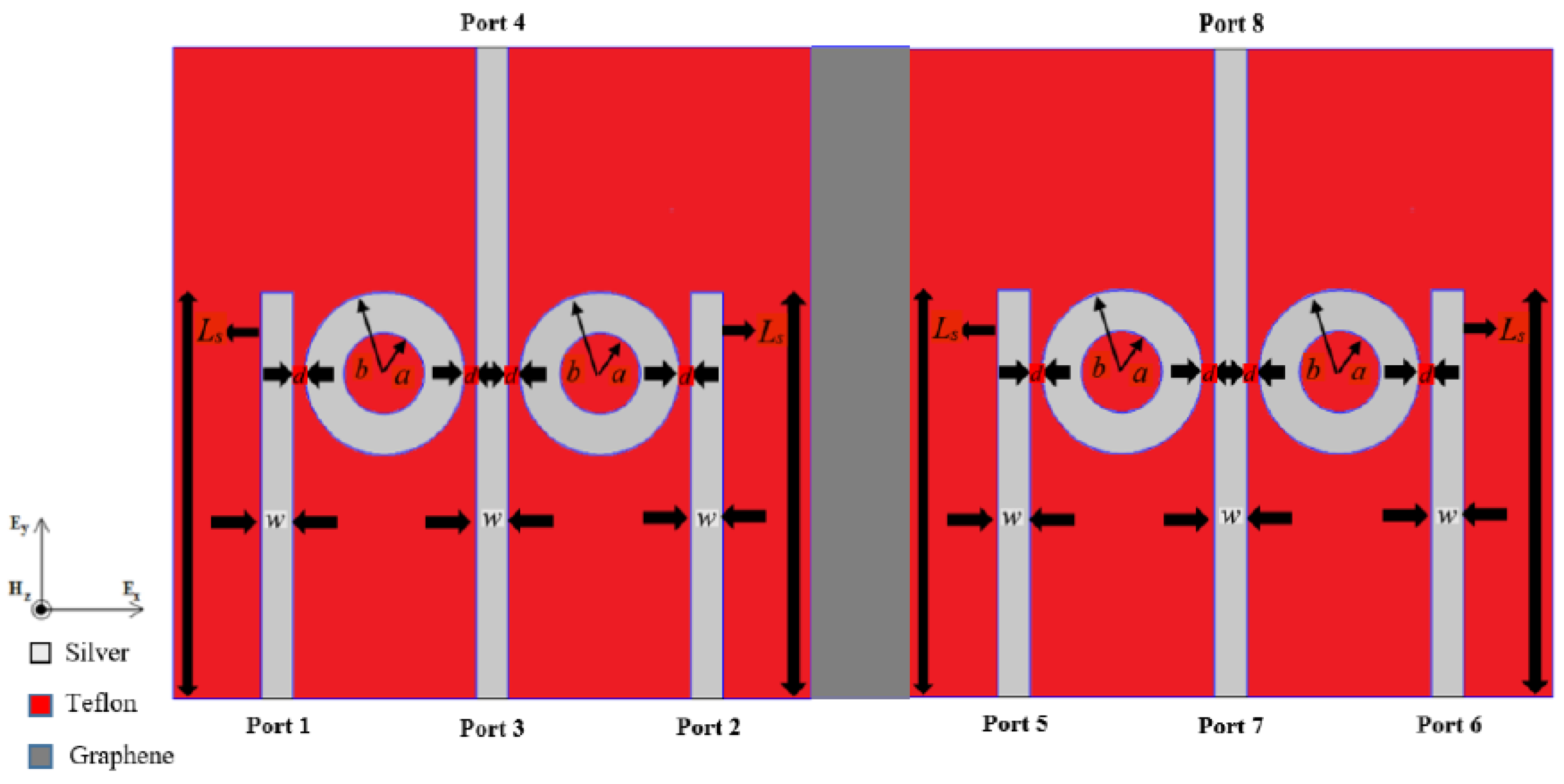
The proposed structure to simulate all-optical plasmonic combinational logic functions (four combinational logic functions) is shown in Figure 1.
The structure that construct four combinational logic functions consists of two sub-structures of dimensions 400 nm × 400 nm separated by 50 nm width of perfect mirror to do the isolation process between the two sub-structures. The perfect mirror can be realized by using graphene material [20,21]. Each sub-structure has three straight stripes and two Nano-rings resonators to give one of the outputs of the proposed plasmonic combinational logic functions based on the IMI plasmonic waveguides. The length of the middle and side stripes (Ls) in each sub-structure are 400 nm and 250 nm, respectively. The width (w) of these stripes is 20 nm, the radii of the Nano-ring resonator (a) and (b) in each sub-structure are 25 nm and 50 nm, respectively, and the coupling distance (d) between the Nano-rings resonator and stripes in each sub-structure is 7.5 nm.
The materials of the proposed structure are silver and Teflon. In our structure, stripes and two Nano-rings in each sub-structure are represented as silver material, while the remaining part of the structure is a Teflon material as shown in Figure 1.
All four proposed plasmonic combinational logic functions have the same dimensions, parameters, and materials in their structures.
In our simulations, Johnson and Christy data is used to describe the silver permittivity [22], while the refractive index of Teflon material is 1.375 [23]. The resonance wavelength of the Nano-rings can be determined by [24,25]:
λsp = 4π neff D
where neff is the effective refractive index and D is the bigger diameter of the Nano-ring. According to Equation (1), the structure parameters and the type of materials play a role in choosing the resonance wavelength. We focus on the resonance wavelength of 1550 nm since this wavelength is the best choice in optical communications applications.
The performance of the proposed plasmonic combinational logic functions is measured by the transmission as a function of wavelengths sweep. The transmission is a ratio between the output optical power to the single input optical power (Input Port or control Port). The transmission is described Equation (2) [26]:
T = Pout ⁄ Pin, (for ON and OFF states of the output Port)
where T is the transmission, Pout is the output optical power of the output Port in ON state and OFF state, and Pin is the input optical power for single Input Port or single control Port.

3. The Proposed All-Optical Combinational Logic Functions

In all four proposed plasmonic combinational logic functions, the structure is illuminated by a plane wave with a wavelength ranging from 1000–2000 nm. This illumination is launched to the Input Port(s) (ON state) and to control Port(s). To use the proposed structure (Figure 1) as a structure to the all four proposed plasmonic combinational logic functions, the Input Port(s), control Port(s), and output Port must be determined to give the function of these proposed plasmonic combinational logic functions. The process of choosing these ports for the proposed plasmonic combinational logic functions is done by trial and error method to give better transmission performance.

3.1. Plasmonic Half-Adder Combinational Logic Circuit

A half-adder is a combinational logic circuit with two inputs and two outputs. The two outputs are the output sum () and the output carry (Cout). The first output () is represented by XOR gate, while the second output (Cout) is represented by AND gate according to Figure 2a,b.
To perform half-adder combinational logic circuit in our structure, we choose the left sub-structure as a structure to perform the output sum and choose the right sub-structure as a structure to perform the output carry. To perform the output sum, we choose Port 1 as an Input Port 1, Port 2 as an Input Port 2, the Output Port is Port 4, and the Control Port is Port 3. To perform the output carry, we choose Port 5 as an Input Port 1, Port 6 as an Input Port 2, the Output Port is Port 7, and the Control Port is Port 8 (see Figure 1).
The function of this combinational logic circuit can be achieved by the constructive and destructive interference between the input signal(s) and the control signal in each sub-structure. When the state of the input ports is OFF and launching light at the wavelength of 1550 nm to the control ports (Port 3 and Port 8) with a Phase equal to 0° always, the state of the output ports is OFF according to the value of transmission that is 0.07 (below transmission threshold = 0.25) for each output. When launching light at the wavelength of 1550 nm to the one Input Port (OFF-ON or ON-OFF states) and to the control ports in the two sub-structures with the same Phase in the output sum structure with control signal and with Phase difference by 180°with control signal in the output carry structure. In these states, the constructive interference will occur in the output sum structure due to the value of transmission that is given by it (T = 0.63) and is regarded as a Logic 1 for these states (OFF-ON or ON-OFF states). On the other hand, the destructive interference will occur in the output carry structure due to the value of transmission that is given by it (T = 0.06) and is regarded as a Logic 0 for these states (OFF-ON or ON-OFF states). In fourth state (ON-ON), the two sub-structures are illuminated by light wave at 1550 nm wavelength in the input ports and control ports. In the output sum structure, the Phases of the input signals are 45° and 180°, respectively. As a result, the destructive interference occurs among the input signals and control signal that is led to make the transmission is low (T = 0.05) that is regarded as Logic 0. In the output carry structure, the Phase of the input signals and control signal is the same (Phase = 0°). As a result, the constructive interference occurs between the two input signals and control signal which makes the transmission is high (T = 0.72) that is regarded as Logic 1. As a result, the function of half-adder combinational logic circuit is achieved. The transmission spectrum of the proposed plasmonic half-adder is shown in Figure 2c. Figure 2d,e show the magnetic field distribution of Logic 00 and Logic 11 inputs plasmonic half-adder, respectively. The operation of the proposed plasmonic half-adder combinational logic circuit is summarized as in Table 1.

3.2. Plasmonic Half-Subtractor Combinational Logic Circuit

A half-subtractor is a combinational logic circuit with two inputs, two outputs, the two outputs are the Difference (D) and the Borrow (B). The first output (D) is represented by XOR gate, while the second output (B) is represented by B logic circuit according to Figure 3a,b.
To perform half-subtrator combinational logic circuit in our structure, we choose the left sub-structure as a structure to perform the Difference (first output) and choose the right sub-structure as a structure to perform the Borrow (second output). To perform the Difference operation, we choose the same ports of output sum structure in half-adder. To perform the Borrow operation, we choose Port 5 as an Input Port 1, Port 6 as an Input Port 2, the Output Port is Port 8, and the Control Port is Port 7 (see Figure 1).
The function of this combinational logic circuit can be achieved by the constructive and destructive interference between the input signal(s) and the control signal in each sub-structure. The Difference operation in this combinational logic circuit is the same of output sum in half-adder combinational logic circuit. The Borrow process is the same of XOR gate but in third state (ON-OFF) the output must be OFF instead of ON state. This state is done by launching light at the wavelength of 1550 nm to the Input Port 1 (Port 5) with a Phase equal to 180° and to the Control Port with a Phase equal to 0° always. The state of the Output Ports is OFF according to the value of transmission that is 0.18 (below transmission threshold = 0.25). As a result, the function of half-subtractor combinational logic circuit is achieved. The transmission spectrum of the proposed plasmonic half-subtractor is shown in Figure 3c. Figure 2d,e show the magnetic field distribution of Logic 10 and Logic 11 inputs plasmonic half-subtractor, respectively. The operation of the proposed plasmonic half-subtractor combinational logic circuit is summarized as in Table 2.

3.3. Plasmonic Comparator One-Bit Combinational Logic Circuit

The basic function of a comparator is to compare the magnitudes of two binary quantities to determine the relationship of those quantities [27]. A comparator is a combinational logic circuit with two inputs, three outputs; the three outputs are the Equality (A = B), the Inequality Less Than (ILT), (A < B), and the Inequality More Than (IMT), (A > B). The first output (Equality) is represented by XNOR gate, while the second and third outputs is merged to gather to represent by XOR gate according to Figure 4a,b.
To perform comparator one-bit combinational logic circuit in our structure, we choose the left sub-structure as a structure to perform the Equality (first output) and choose the right sub-structure as a structure to perform the Inequality (merged second and third outputs). To perform the Equality, we choose Port 2 as an Input Port 1, Port 3 as an Input Port 2, the Output Port is Port 4, and the Control Port is Port 1. To perform the Inequality, we choose Port 5 as an Input Port 1, Port 6 as an Input Port 2, the Output Port is Port 8, and the Control Port is Port 7 (see Figure 1).
The function of this combinational logic circuit can occur by the constructive and destructive interference between the input signal(s) and the control signal in each sub-structure. The operation of the Inequality in this combinational logic circuit is the same of Sum operation and Difference operation in half-adder and half-subtractor combinational logic circuit, respectively. The output of proposed plasmonic Inequality is regarded as the functions of the (ILT), (A < B), in second state and the (IMT), (A > B), in third state. To perform the Equality process, the XNOR gate must be achieved. The first state (OFF-OFF) can be achieved when launching light at the wavelength of 1550 nm to the Control Port with a Phase equal to 180°, the state of the Output Port is ON according to the value of transmission that is 0.2807 (above transmission threshold = 0.25). In the second and the third states (OFF-ON or ON-OFF), the destructive interference happened between the input signal and control signal due to the difference in Phase. Therefore, the transmission is less than the threshold and regarding it as Logic 0. In the fourth state (ON-ON), the large constructive interference happened between input signals and control signal due to the Phase of these signals is similar (Phase = 180°). This resulted to enhance the transmission above 100% (175%) and that is regarded as Logic 1. As a result, the function of comparator one-bit combinational logic circuit is achieved. The transmission spectrum of the proposed plasmonic comparator one-bit is shown in Figure 4c. Figure 4d–g show the magnetic field distribution of Logic 00, 01, 10 and 11 inputs plasmonic comparator one-bit, respectively. The operation of the proposed plasmonic comparator one-bit combinational logic circuit is summarized as in Table 3.

3.4. Plasmonic Full-Adder Combinational Logic Circuit

The full-adder accepts two input bits and an input carry and generates an output sum and an output carry [27]. A full-adder is a combinational logic circuit with three inputs (A, B, and Ci), two outputs, the two outputs are the output sum () and the output carry (Cout) according to Figure 5a,b.
To perform full-adder combinational logic circuit in our structure, we choose the left sub-structure as a structure to perform an output sum (first output) and choose the right sub-structure as a structure to perform an output carry (second output). The assigning of the input ports for the two sub-structures is shown in Table 4 (see Figure 1).
The function of this combinational logic circuit can be achieved by the constructive and destructive interference between the input signals in each sub-structure. When the one of Input Ports is in ON state (OFF-OFF-ON, OFF-ON-OFF, or ON-OFF-OFF), only the output sum is in ON state according to the value of transmission that is 0.2807 (above transmission threshold = 0.25) for three states. While, the output carry is OFF in these states according to the value of transmission that is 0.07 (below transmission threshold = 0.25) for three states. In forth state (OFF-ON-ON), only output carry is in ON state according to the value of transmission that is 1.12 (above transmission threshold = 0.25). While, the output sum is OFF according to the value of transmission that is 0.002 (below transmission threshold = 0.25). In sixth and seventh states (ON-OFF-ON or ON-ON-OFF), also the output carry is in ON state according to the value of transmission that is 0.63 (above transmission threshold = 0.25). While, the output sum is OFF according to the value of transmission that is 0.07 (below transmission threshold = 0.25). In eighth state (ON-ON-ON), both outputs are in ON state according to the value of transmission that is 1.75 (above transmission threshold = 0.25). The constructive and destructive interferences occur when the Phase of input signals is the same or is the different, respectively. As a result, a full-adder combinational logic circuit is achieved without construction their internal logic gates. The transmission spectrum of the proposed plasmonic full-adder is shown in Figure 5c. Figure 5d–g show the magnetic field distribution of Logic 001, 011, 110 and 111 inputs plasmonic full-adder, respectively. The operation of the proposed plasmonic full-adder combinational logic circuit is summarized as in Table 5.

4. The Comparison between the Proposed Work and the Previous Works

The proposed plasmonic combinational logic functions are compared to the previous papers as depicted in Table 6.

5. Conclusions

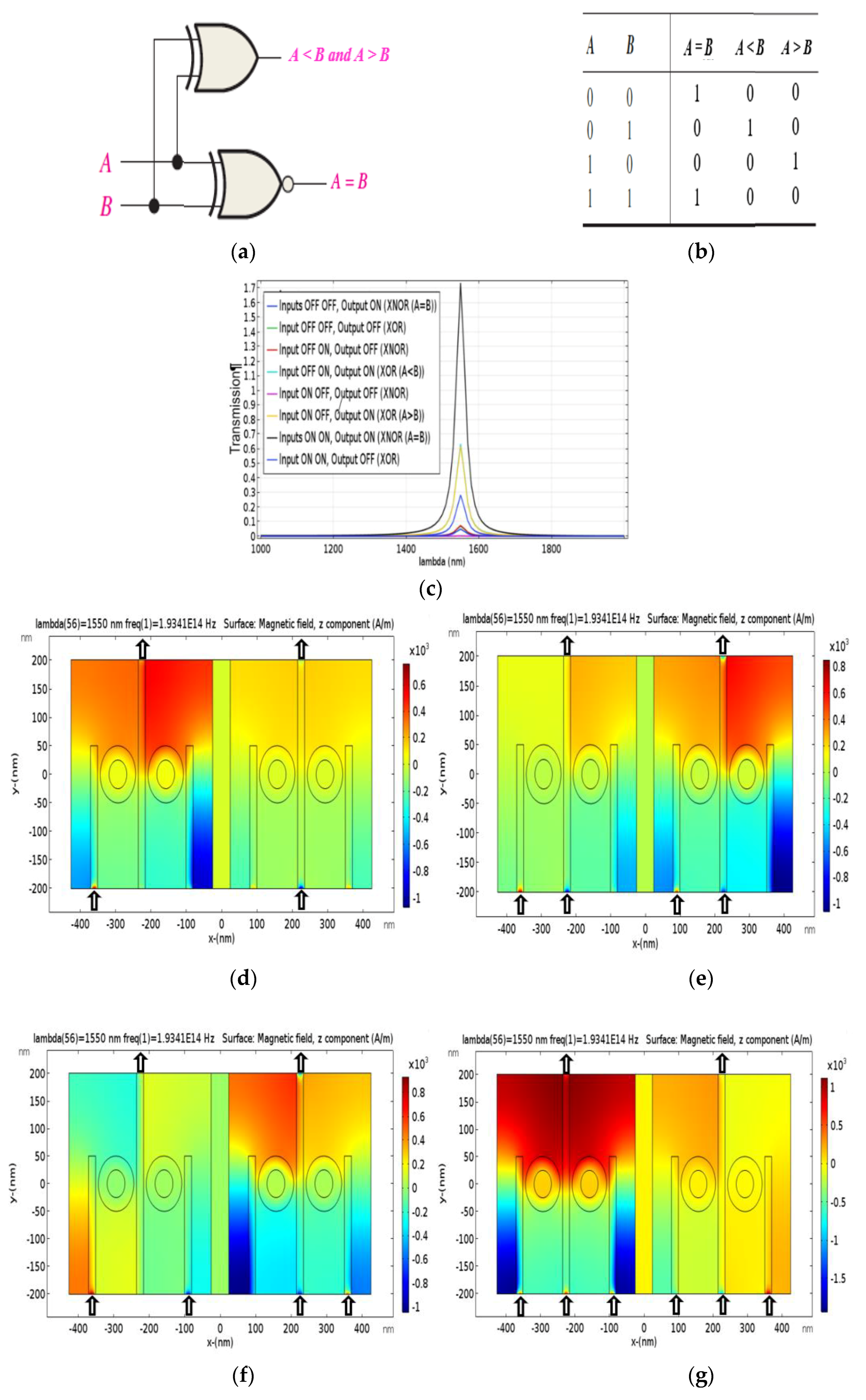
In this paper, four plasmonic combinational logic functions have been proposed, designed and simulated using 2-D FEM. These combinational logic functions are half-adder, half-subtractor, comparator one-bit, and full-adder. The combinational logic functions are constructed by Nano-rings IMI plasmonic structure. By employing the coupling property between straight stripes and ring resonator waveguides, we can achieve a plasmonic combinational logic function. By changing the state of the Input Port(s), the position of the Input Port(s) and a Control Port(s), and the Phase of incident light in these ports, we can make the transmission in the Output Port minimized or maximized according to the required plasmonic combinational logic function. To give a decision that the proposed plasmonic combinational logic function is investigating the truth table of one of the combinational logic functions, we have established a threshold value of transmission to distinguish between Logic 1 and Logic 0 states. The proposed value of transmission threshold is 0.25 or 25%; choosing this value achieves four plasmonic combinational logic functions in one structure. Finally, the proposed plasmonic combinational logic functions are considered fundamental building blocks in photonic integrated circuits and all-optical signal processing systems, and pave a way to achieve ultra-high-speed optical chip circuits.

Author Contributions

This Research Conceptualization is done by M.N.A. and the methodology is done by S.H.A. and M.N.A. using Comsol Multiphysics 5.3 Software; Validation is done by S.H.A. and M.N.A.; Formal analysis is done by S.H.A. and M.N.A.; Investigation is done by S.H.A. and M.N.A.; Resources are done by S.H.A. and M.N.A.; Data curation is done by S.H.A. and M.N.A.; Writing-Original Draft Preparation is done by S.H.A.; Writing-Review & Editing is done by M.N.A.; Visualization is done by S.H.A. and M.N.A.; Supervision is done by M.N.A.; Project Administration is done by M.N.A.; Funding Acquisition is done by ourselves.

Funding

This research received no external funding.

Conflicts of Interest

The authors declare no conflict of interest.

References

  1. Lezec, H.J.; Degiron, A.; Devaux, E.; Linke, R.A.; Martin-Moreno, L.; Garcia-Vidal, F.J.; Ebbesen, T.W. Beaming light from a subwavelength aperture. Science 2002, 297, 820–822. [Google Scholar] [CrossRef] [PubMed]
  2. Fu, Y.; Hu, X.; Lu, C.; Yue, S.; Yang, H.; Gong, Q. All-optical logic gates based on nanoscale plasmonic slot waveguides. Nano Lett. 2012, 12, 5784–5790. [Google Scholar] [CrossRef] [PubMed]
  3. Yu, S.; Piao, X.; Park, N. Slow-light dispersion properties of multiatomic multiband coupled-resonator optical waveguides. Phys. Rev. A 2012, 85, 023823. [Google Scholar] [CrossRef]
  4. Yu, S.; Piao, X.; Park, N. Controlling random waves with digital building blocks based on supersymmetry. Phys. Rev. Appl. 2017, 8, 054010. [Google Scholar] [CrossRef]
  5. Dolatabady, A.; Granpayeh, N. All optical logic gates based on two dimensional plasmonic waveguides with nanodisk resonators. J. Opt. Soc. Korea 2012, 16, 432–442. [Google Scholar] [CrossRef]
  6. Wu, Y.D.; Hsueh, Y.T.; Shih, T.T. Novel all-optical logic gates based on microring metal-insulator-metal plasmonic waveguides. In Proceedings of the 2013 PIERS Proceedings, Taipei, Taiwan, 25–28 March 2013; pp. 169–172. [Google Scholar]
  7. Nozhat, N.; Granpayeh, N. All-optical logic gates based on nonlinear plasmonic ring resonators. Appl. Opt. 2015, 54, 7944–7948. [Google Scholar] [CrossRef] [PubMed]
  8. Dolatabady, A.; Granpayeh, N. All-optical logic gates in plasmonic metal–insulator–metal nanowaveguide with slot cavity resonator. J. Nanophoton. 2017, 11, 026001. [Google Scholar] [CrossRef]
  9. Liu, Z.; Ding, L.; Yi, J.; Wei, Z.; Guo, J. Design of a multi-bits input optical logic device with high intensity contrast based on plasmonic waveguides structure. Opt. Commun. 2019, 430, 112–118. [Google Scholar] [CrossRef]
  10. Khosroshahi, H.R.; Baghban, H. Design and Analysis of Plasmonic Half-Adder Based on Metal Slot Waveguide. In Proceedings of the Iranian Conference on Optics & Photonics, Shahid Beheshti University, Tehran, Iran, 13–15 January 2015; Optics and Photonics Society of Iran: Tehran, Iran, 2015. [Google Scholar]
  11. Birr, T.; Zywietz, U.; Chhantyal, P.; Chichkov, B.N.; Reinhardt, C. Ultrafast surface plasmon-polariton logic gates and half-adder. Opt. Express 2015, 23, 31755–31766. [Google Scholar] [CrossRef] [PubMed]
  12. Janipour, M.; Karami, M.A.; Zia, A. Plasmonic adder/subtractor module based on a ring resonator filter. Iran. J. Electr. Electron. Eng. 2016, 12, 113–118. [Google Scholar]
  13. Kumar, S.; Singh, L.; Chen, N.K. All-optical bit magnitude comparator device using metal–insulator–metal plasmonic waveguide. Opt. Eng. 2017, 56, 121908. [Google Scholar] [CrossRef]
  14. Xiea, J.; Niua, X.; Hu, X.; Wang, F.; Chai, Z.; Yang, H.; Gong, Q. Ultracompact all-optical full-adder and half-adder based on nonlinear plasmonic nanocavities. Nanophotonics 2017, 6, 1161–1173. [Google Scholar] [CrossRef] [Green Version]
  15. Kumar, S.; Singh, L.; Raghuwanshi, S.K. Design of Plasmonic Half-Adder and Half-Subtractor Circuits Employing Nonlinear Effect in Mach–Zehnder Interferometer; Springer: Berlin/Heidelberg, Germany, 2016. [Google Scholar]
  16. Yu, S.; Piao, X.; Koo, S.; Shin, J.H.; Lee, S.H.; Min, B.; Park, N. Mode junction photonics with a symmetry breaking arrangement of mode-orthogonal heterostructures. Opt. Express 2011, 19, 25500–25511. [Google Scholar] [CrossRef] [PubMed]
  17. Serajmohammadi, S.; Alipour-Banaei, H.; Mehdizadeh, F. Proposal for realizing an all-optical half adder based on photonic crystals. Appl. Opt. 2018, 57, 1617–1621. [Google Scholar] [CrossRef] [PubMed]
  18. Gayen, D.K.; Chattopadhyay, T.; Bhattacharyya, A.; Basak, S.; Dey, A.D. All-optical half-adder/half-subtractor using terahertz optical asymmetric demultiplexer. Appl. Opt. 2014, 53, 8400–8409. [Google Scholar] [CrossRef] [PubMed]
  19. Jiang, H.; Chen, Y.; Li, G.; Zhu, C.; Chen, A.X. Optical half-adder and half-subtracter employing the pockels effect. Opt. Express 2015, 23, 9784–9789. [Google Scholar] [CrossRef] [PubMed]
  20. Jornet, J.M.; Akyildiz, I.F. Graphene-based plasmonic nano-antenna for terahertz band communication in nanonetworks. IEEE J. Sel. Areas Commun. Suppl. Part 2 2013, 31, 685–694. [Google Scholar] [CrossRef]
  21. Anku, W.W.; Kiarii, E.M.; Sharma, R.; Joshi, G.M.; Shukla, S.K.; Govender, P.P. Photocatalytic Degradation of Pharmaceuticals Using Graphene Based Materials. In A New Generation Material Graphene: Applications in Water Technology; Naushad, M., Ed.; Springer: Basel, Switzerland, 2019; pp. 187–208. [Google Scholar]
  22. Johnson, P.B.; Christy, R.W. Optical constants of the noble metals. Phys. Rev. 1972, 6, 4370–4379. [Google Scholar] [CrossRef]
  23. French, R.H.; Rodríguez-Parada, J.M.; Yang, M.K.; Derryberry, R.A.; Lemon, M.F.; Brown, M.J.; Haeger, C.R.; Samuels, S.L.; Romano, E.C.; Richardson, R.E. Optical properties of materials for concentrator photovoltaic systems. In Proceedings of the 2009 34th IEEE Photovoltaic Specialists Conference (PVSC), Philadelphia, PA, USA, 7–12 June 2009; pp. 394–399. [Google Scholar]
  24. Chowdhury, Y. Plasmonic Waveguides: Design and Comparative Study. Master’s Thesis, Royal Institute of Technology, Stockholm, Sweden, 2011. [Google Scholar]
  25. Maradudin, A.A.; Sambles, J.R.; Barnes, W.L. Modern Plasmonics; Elsevier: Amsterdam, The Netherlands, 2014. [Google Scholar]
  26. Lin, X.S.; Huang, X.G. Tooth-shaped plasmonic waveguide filters with nanometeric sizes. Opt. Lett. 2008, 33, 2874–2876. [Google Scholar] [CrossRef] [PubMed]
  27. Floyd, T.L. Digital Fundamentals, 11th ed.; Pearson Education: London, UK, 2015. [Google Scholar]
Figure 1. The proposed structure for the proposed plasmonic four combinational logic functions.
Photonics 06 00030 g001
Figure 2. (a,b) the conventional half-adder logic diagram and its truth table, respectively. (c) The transmission spectrum of the proposed plasmonic half-adder for different states, according to its truth table. (d,e) the magnetic field distribution of Logic 00 and Logic 11 inputs, respectively.
Photonics 06 00030 g002
Figure 3. (a,b) the conventional half-subtractor logic diagram and its truth table, respectively. (c) The transmission spectrum of the proposed plasmonic half-subtractor for different states, according to its truth table. (d,e) the magnetic field distribution of Logic 10 and Logic 11 inputs, respectively.
Photonics 06 00030 g003
Figure 4. (a) and (b) the conventional comparator one-bit logic diagram and its truth table, respectively. (c) The transmission spectrum of the proposed plasmonic comparator one-bit for different states, according to its truth table. (d), (e), (f) and (g) the magnetic field distribution of Logic 00, 01, 10, and 11 inputs, respectively.
Photonics 06 00030 g004
Figure 5. (a) and (b) the conventional full-adder logic symbol and its truth table, respectively. (c) The transmission spectrum of the proposed plasmonic full-adder for different states, according to its truth table. (d), (e), (f) and (g) the magnetic field distribution of Logic 001, 011, 110, and 111 inputs, respectively.
Photonics 06 00030 g005
Table 1. Operation of the transmission for the proposed plasmonic half-adder.
(a)
(a)
InputInputInput 1Input 2Input 1Input 2
State 1State 2Port 1Port 2Port 5Port 6
(Phase)(Phase)(Phase)(Phase)
Logic 0Logic 0OFF (0 ° )OFF (0 ° )OFF (0 ° )OFF (0 ° )
Logic 0Logic 1OFF (0 ° )ON (0 ° )OFF (0 ° )ON (0 ° )
Logic 1Logic 0ON (0 ° )OFF (0 ° )ON (0 ° )OFF (0 ° )
Logic 1Logic 1ON (45 ° )ON (180 ° )ON (0 ° )ON (0 ° )
(b)
(b)
ControlControlT (Port 4)T (Port 7)TthreshSumOutputOutputOutput
Port 3Port 8 OutputCarryPort 4Port 7
(Phase)(Phase)
ON (0 ° )ON (0 ° )0.070.070.25Logic 0Logic 0OFFOFF
ON (0 ° )ON (0 ° )0.620.060.25Logic 1Logic 0ONOFF
ON (0 ° )ON (0 ° )0.630.060.25Logic 1Logic 0ONOFF
ON (0 ° )ON (0 ° )0.050.720.25Logic 0Logic 1OFFON
Table 2. Operation of the transmission for the proposed plasmonic half-subtractor.
(a)
(a)
InputInputInput 1Input 2Input 1Input 2
State 1State 2Port 1Port 2Port 5Port 6
(Phase)(Phase)(Phase)(Phase)
Logic 0Logic 0OFF (0 ° )OFF (0 ° )OFF (0 ° )OFF (0 ° )
Logic 0Logic 1OFF (0 ° )ON (0 ° )OFF (0 ° )ON (0 ° )
Logic 1Logic 0ON (0 ° )OFF (0 ° )ON (180 ° )OFF (0 ° )
Logic 1Logic 1ON (45 ° )ON (180 ° )ON (180 ° )ON (45 ° )
(b)
(b)
ControlControlT (Port 4)T (Port 8)TthreshDBorrowOutputOutput
Port 3Port 8 OutputCarryPort 4Port 8
(Phase)(Phase)
ON (0 ° )ON (0 ° )0.070.070.25Logic 0Logic 0OFFOFF
ON (0 ° )ON (0 ° )0.620.630.25Logic 1Logic 1ONON
ON (0 ° )ON (0 ° )0.630.180.25Logic 1Logic 0ONOFF
ON (0 ° )ON (0 ° )0.050.050.25Logic 0Logic 0OFFOFF
Table 3. Operation of the transmission for the proposed plasmonic comparator.
(a)
(a)
InputInputInput 1Input 2Input 1Input 2ControlControl
State 1State 2Port 2Port 3Port 5Port 6Port 1Port 7
(Phase)(Phase)(Phase)(Phase)(Phase)(Phase)
Logic 0Logic 0OFF (0 ° )OFF (0 ° )OFF (0 ° )OFF (0 ° )ON (180 ° )ON (0 ° )
Logic 0Logic 1OFF (0 ° )ON (0 ° )OFF (0 ° )ON (0 ° )ON (180 ° )ON (0 ° )
Logic 1Logic 0ON (0 ° )OFF (0 ° )ON (180 ° )OFF (0 ° )ON (180 ° )ON (0 ° )
Logic 1Logic 1ON (45 ° )ON (180 ° )ON (180 ° )ON (45 ° )ON (180 ° )ON (0 ° )
(b)
(b)
T (Port 4)T (Port 8)TthreshA = BA > B and B > AOutputOutput
OutputOutputPort 4Port 8
0.28250.070.25Logic 1Logic 0ONOFF
0.070.630.25Logic 0Logic 1OFFON
0.0020.620.25Logic 0Logic 1OFFON
1.750.050.25Logic 1Logic 0ONOFF
Table 4. Assigning input signals to ports of the outputs of the proposed plasmonic full-adder.
Assigning Input Signals to Ports for the Sum Output (∑)Assigning Input Signals to Ports for the Output Carry (Cout)
Port 1Port 2Port 3Port 5Port 6Port 7
CiBACiBA
CiBAABCi
CiBACiAB
CiBACiBA
ABCiCiBA
CiBACiBA
CiBACiBA
CiBACiBA
Table 5. Operation of the transmission for the proposed plasmonic full-adder.
(a)
(a)
InputInputInputInput 1Input 2Input 3Input 1Input 2Input 3
State 1State 2State 3(Phase)Port 2(Phase)(Phase)(Phase)(Phase)
(Phase)
Logic 0Logic 0Logic 0OFF (0 ° )OFF (0 ° )OFF (0 ° )OFF (0 ° )OFF (0 ° )OFF (0 ° )
Logic 0Logic 0Logic 1OFF (0 ° )OFF (0 ° )ON (0 ° )OFF (0 ° )OFF (0 ° )ON (0 ° )
Logic 0Logic 1Logic 0OFF (0 ° )ON (0 ° )OFF (0 ° )OFF (0 ° )ON (0 ° )OFF (0 ° )
Logic 0Logic 1Logic 1OFF (0 ° )ON (180 ° )ON (45 ° )OFF (0 ° )ON (0 ° )ON (0 ° )
Logic 1Logic 0Logic 0ON (0 ° )OFF (0 ° )OFF (0 ° )ON (0 ° )OFF (0 ° )OFF (0 ° )
Logic 1Logic 0Logic 1ON (180 ° )OFF (0 ° )ON (45 ° )ON (0 ° )OFF (0 ° )ON (0 ° )
Logic 1Logic 1Logic 0ON (180 ° )ON (45 ° )OFF (0 ° )ON (0 ° )ON (0 ° )OFF (0 ° )
Logic 1Logic 1Logic 1ON (0 ° )ON (0 ° )ON (0 ° )ON (0 ° )ON (0 ° )ON (0 ° )
(b)
(b)
T (Port 4)T (Port 8)TthreshSumOutputOutputOutput
OutputCarryPort 4Port 8
000.25Logic 0Logic 0OFFOFF
0.28250.070.25Logic 1Logic 0ONOFF
0.2740.070.25Logic 1Logic 0ONOFF
0.021.120.25Logic 0Logic 1OFFON
0.28970.070.25Logic 1Logic 0ONOFF
0.070.620.25Logic 0Logic 1OFFON
0.070.630.25Logic 0Logic 1OFFON
1.741.740.25Logic 1Logic 1ONON
Table 6. Comparison between our proposed plasmonic combinational logic functions and previous papers.
Criteria/Article)This ArticleRef. [10]Ref. [11]Ref. [12]Ref. [13]Ref. [14]
Software Program UsedFEM-2DFEM-2DFinite Difference Time FEM-2D DomainFinite Difference Time FEM-2D DomainFinite Difference Time FEM-2D DomainFEM-2D
Proposed StructureNano-Rings Insulator-Metal-Insulator (IMI) Plasmonic Nano-WaveguidesPlasmonic Metal Slot WaveguidesLinear Interference Effects in Dielectric Crossed Waveguide StructureRing Resonator Based Metal–Insulator–Metal (MIM) Plasmonic WaveguidesMach–Zehnder Interferometer (MZI) Using a Plasmonic MIM WaveguidesNonlinear Plasmonic Nanoca vities
Number of Proposed Combinational Logic Functions4 Combinational Logic Functions1 Combinational Logic Functions1 Combinational Logic Functions2 Combinational Logic Functions1 Combinational Logic Functions1 Combinational Logic Functions
Proposed Combinational Logic FunctionsHalf-Adder, Half-Subtractor, Comparator One-Bit, and Full-AdderHalf-AdderHalf-AdderHalf-Adder and Half-SubtractorCompar ator One-BitHalf-Adder Full-Adder
Size850 nm × 400 nmNot Available10 µm × 28 µmMore than 1260 nm × 1260 nm17 µm × 3 µmLess than 15 µm × 15 µm
Operating Wave-Length (s)1550 nm530 nm800 nm630 nm, 901 nm, 1770 nm, and 1856 nm1550 nm750 nm and 770 nm
Dielectric Material UsedTeflonSiO2Organically Modified Silica (ORMOSIL)AirNon-Linear Kerr MaterialAir
Nobel Material UsedSilverGoldGoldSilverSilverGold
Model of Description the Relative Permittivity of the MetalJohnson and Christy DataNot AvailableNot AvailableDrude–Lorentz ModelDrude–Lorentz ModelNot Available
Performance MeasuredTransmissionOutput Optical PowerIntensityTransmissionIntensityTransmission and Contrast Ratio

