1. Introduction
The design of devices able to dissipate all the energy of an impinging electromagnetic wave into heat or other forms of energy, i.e., absorbers, has a long history that can be dated back to the World War II [
1]. Nowadays, the use of RF and microwave absorbers is consolidated in many fields, such as electronic warfare and stealth technology [
1], electromagnetic measurements [
2], and antenna systems [
3]. In the last few decades, there has been an increasing interest in extending similar effects to the visible spectrum [
4,
5,
6,
7,
8,
9,
10,
11,
12,
13,
14,
15]. Optical absorption, in fact, plays a key role in many relevant applications, including photovoltaics and thermophotovoltaics [
16], photodetectors [
17], color filters [
18], and thermal light sources [
19].
Recently, we have discussed the possibility to engineer the surface dispersion of small nanoparticles to achieve large optical absorption [
20,
21]. It is known that when the size of a plasmonic nanoparticle is smaller than the mean free path of electrons, its optical losses increase compared to the ones of the bulk material due to the additional scattering of electrons at the nanoparticle boundaries [
22]. The arrangement of such small nanoparticles in an array configuration enables the design of ultrathin resistive sheets with a controlled amount of losses at a given frequency of the optical spectrum. Based on this concept, we have proposed an optical implementation of a Salisbury screen [
20] and a possible variant featuring transparency outside its absorption bandwidth [
21].
The aim of this contribution is to explore the suitability of nanoparticle arrays for the design of an advanced class of optical absorbers, i.e., the so-called circuit-analog (CA) absorbers. CA absorbers are popular at microwaves [
23] for their larger absorption bandwidth compared to an equally thick Salisbury screen. The wider frequency response is obtained by replacing the resistive sheet with several reactive lossy layers that are able to compensate for the intrinsic reactance of the grounded dielectric around the resonance frequency of the structure. As we show in the following, arrays of plasmonic nanoparticles can be engineered to behave both as a resistive and a reactive layer and, thus, are suitable candidates for implementing CA absorbers in the visible spectrum.
We will show that, by exploiting the proposed approach, it is possible to design a three-layered CA absorber whose absorption bandwidth is 6 times bigger than the one of an optical Salisbury screen of equal thickness. Different from the conventional broadband solutions available in the market, the proposed absorbers are fully compatible with modern nanophotonic components and devices.
2. Materials and Methods
A CA absorber is a grounded structure consisting of
N reactive layers separated by dielectric spacers [
1]. Its geometry for
N = 3 is sketched in
Figure 1a. We assume that the absorber is illuminated by a transverse-magnetic (TM) plane wave whose wave vector
ki forms an angle
θ with the
z-axis. The dielectric spacers have relative permittivity and permeability (
εi,
μi), whereas each reactive layer is characterized by a surface impedance
Zs =
Rs +
jXs, whose real and imaginary parts account for the electromagnetic losses and the reactive behavior of the sheet, respectively.
The easiest strategy to design a CA absorber relies on the use of the Smith chart [
23]. However, as it will be clear later, the strong frequency-dispersion of the nanoparticle-based optical resistive sheets limits the applicability of this simple approach in our scenario. An equivalent transmission-line representation of the device, such as the one shown in
Figure 1b, is more convenient for our purposes. In this formalism, the
i-th dielectric spacer is represented by a transmission line with length
di and characteristic impedance
ηi, whereas each reactive layer is modeled through a shunt lumped impedance
Zsi.
The secondary constants of each transmission line segment, i.e., its characteristic impedance
ηi and propagation constant
βi, can be written in the following form:
where
ω is the angular frequency and
kx is the
x-component of the free-space wave vector that is equal to
For a normal-incident wave, the propagation constant of the i-th transmission line βi is equal to the dielectric wavenumber .
The design of a CA absorber involves the maximization of the absorption coefficient within a desired range of frequencies. Since CA absorbers are terminated on a ground plane and, thus, their transmission coefficient is zero, the maximization of the absorption corresponds to the minimization of the input reflection coefficient. By relying on the model shown in
Figure 1b, the input reflection coefficient can be easily calculated using the conventional transmission line formulas. In particular, the input impedance of a load
ZL at a given
z can be calculated as [
24]:
Using Equation (3), it is easy to calculate the line impedance before the first reactive layer:
Such an impedance is shunt-connected to the surface impedance of the reactive layer and, thus, the overall impedance at
z =
d1 is equal to
These simple analytical steps can be recursively applied to the two subsequent dielectric spacers and shunt layers in order to calculate the overall input impedance
Zin at
z =
d1 +
d2 +
d3. Once
Zin is known, the input reflection coefficient can be expressed as follows:
where
η0 = 377 Ω is the free-space impedance. The above procedure can be easily extended to a CA absorber made by an arbitrary number of layers
N or even to non-homogenous dielectric layers [
25,
26].
Before moving forward, it is necessary to specify how to implement the reactive layers required by a CA absorber at optical frequencies. At microwaves, such layers can be realized by patterning a lossy material [
27,
28] or by adding lossy lumped elements to a reactive surface [
29]. As to the optical frequencies, we have recently proven that a resistive sheet can be realized using an array of ellipsoidal nanoparticles that are smaller than the mean free path of electrons in the constituent plasmonic material [
20]. However, we have also shown that, by properly tuning the eccentricity of the nanoparticles and their separation distance, it is possible to add a capacitive or inductive behavior to the lossy array [
30,
31,
32].
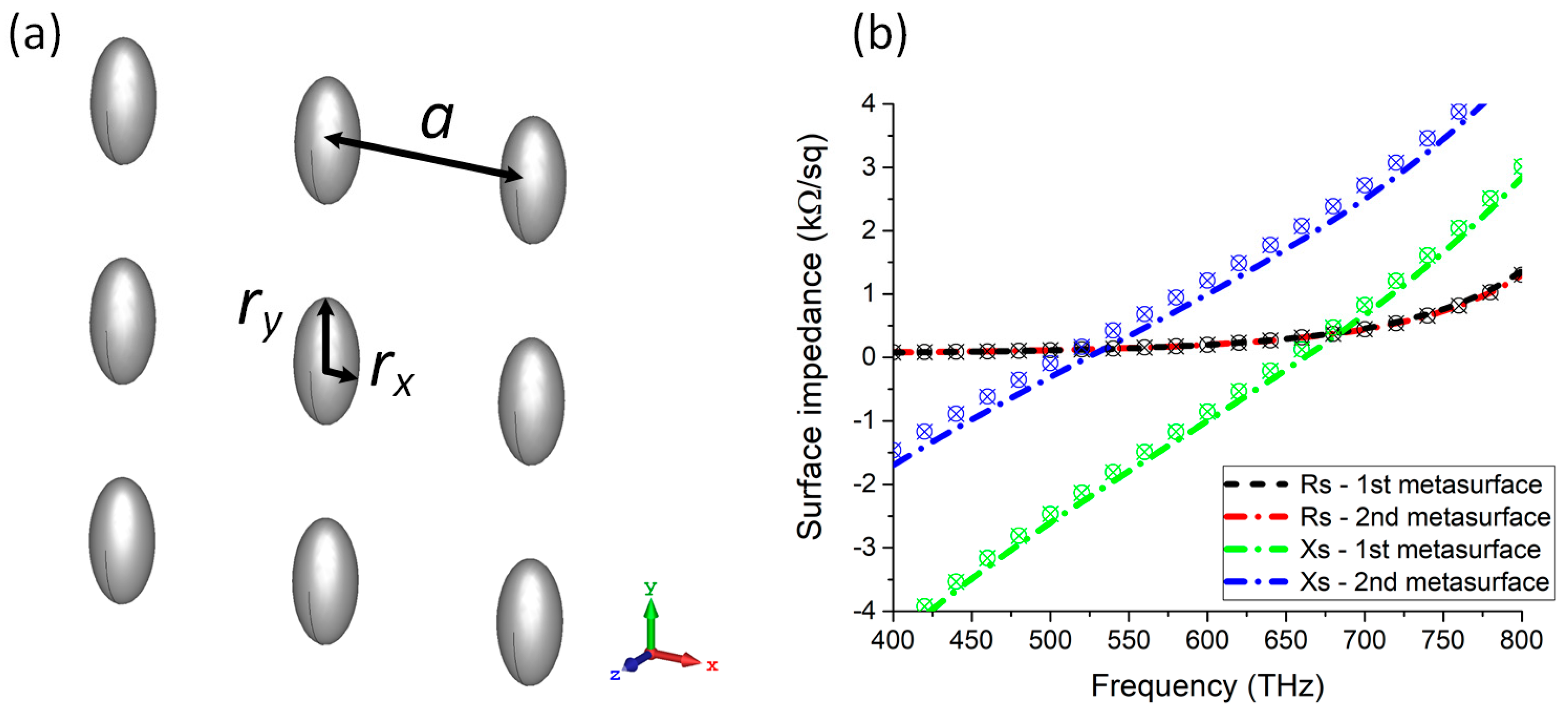
In this paper, thus, the reactive layers are implemented through a square array of nanoparticles, such as the one shown in
Figure 2a. The nanoparticles are prolate spheroids with
rx =
rz and they are made of silver. Their permittivity is expressed through the following size-corrected dielectric function [
33]:
The values of the parameters appearing in Equation (7) are ωp = 9.17 eV, ωL = 5.27 eV, f = 2.2, ΓL = 1.14 eV, γ = 0.0023 × ωp, vF = 1.39 × 10⁶ m/s, A = 0.6. It is important to underline that, compared to the conventional Drude model of silver, Equation (7) contains an additional loss contribution that is inversely proportional to the radius of the nanoparticle. This term accounts for the surface dispersion that allows tuning the surface resistance of the nanoparticle array.
By assuming that the size of the nanoparticles and their separation distance are significantly smaller than the operative wavelength, the structure in
Figure 2a can be homogenized through effective bulk or surface parameters. There exist several alternative methods for describing the optical behavior of the structure shown in
Figure 2a, such as volumetric homogenization [
34,
35] and equivalent conductivity methods [
36]. However, the approach based on the definition of an effective surface impedance is the most suitable for the design of ultra-thin layers exhibiting both resistive and reactive behaviors. According to it, when illuminated by an external normally-impinging plane wave with the electric field parallel to the major axis of the ellipsoids, the structure shown in
Figure 2a behaves as a lossy reactive layer, whose surface impedance is [
20]
where
a is the separation distance among nanoparticles,
αy the
y-component of the nanoparticle polarizability tensor [
22],
the wavenumber in the hosting material, and, finally,
β is the interaction constant among nanoparticles. An approximate expression for
β for the case of normal incidence is available, for instance, in Reference [
37].
By exploiting the Equation (8), we have analytically designed two different metasurfaces exhibiting the same surface resistance (
Rs = 200 Ω) but opposite surface reactance (
Xs1 = −1000 Ω/sq and
Xs2 = 1000 Ω/sq, respectively) at
f = 600
THz. Their dimensions are as follows: (1st)
ry = 16 nm,
rx = 6 nm,
a = 55 nm; (2nd)
ry = 22 nm,
rx = 5 nm,
a = 55 nm. The frequency behavior of the complex surface impedance for these arrays of nanoparticles is shown in
Figure 2b. The ticks represent the numerical values that have been retrieved through full-wave simulations. As can be appreciated, such a configuration allows achieving a non-resonant lossy behavior at a desired frequency of the visible spectrum. Specifically, the surface reactance is mainly related to the nanoparticle eccentricity, whereas the surface resistance can be tuned by acting on the absolute size of the nanoparticles [
20]. Thus, by engineering the major and minor axes of the nanoparticles, it is possible to obtain an optical metasurface with a desired amount of losses and either a capacitive or an inductive behavior. It is interesting to observe that, differently from their microwave versions, the surface impedance of an optical metasurface based on nanoparticles is strongly frequency-dispersive, even in its real part. This implies that the maximum achievable bandwidth of a nanoparticles-based optical absorber is unavoidably lower than the one of a corresponding CA absorber working at microwave frequencies.
By introducing Equation (8) into the reflection coefficient (6), we can find an analytical expression of the reflection coefficient that depends on the dimensions of the different nanoparticle arrays composing the CA absorber. As we will show in the next Section, this expression can be analytically minimized within the desired range of frequencies of the optical spectrum with respect to the geometrical parameters of the structure.
Before concluding this Section, we would like to underline that, given the geometrical and electromagnetic anisotropy of the ellipsoids composing the optical metasurfaces, their response is intrinsically polarization-sensitive, i.e., they exhibit different values of surface resistance and reactance depending on the orientation of the incident electric field. While we have shown that it is possible to make these structures quasi-isotropic by properly arranging different replicas of the nanoparticles [
20], we also remark that such a feature can be considered an advantage in several applications, such as the design of optical polarizers or polarization-sensitive devices.
3. Results
In the previous Section, we discussed an analytical model able to describe the behavior of a CA absorber whose lossy reactive layers are implemented through plasmonic nanoparticle arrays. Here, we show how this model can be exploited for designing a wideband optical absorber.
The design of a CA absorber is based on the numerical minimization of the discrete frequency integral of the reflection coefficient (6) with respect to the design parameters, i.e., the dimensions of the two arrays of nanoparticles and the thicknesses of the dielectric spacers:
However, to ensure the physical realizability of the absorber, some design constraints must be imposed to Equation (9): first, the separation distance among the nanoparticles must be greater than twice the major axis, i.e., a > 2ry; then, we may want to take into account the limitations of the most common nanofabrication facilities and force a minimum nanoparticle size, i.e., . Moreover, in order to minimize the coupling between metasurfaces that may affect their effective surface impedance, we need to impose that the two nanoparticle arrays have a minimum separation, i.e., d1, d2 > λ/15, λ being the wavelength inside the dielectric at the central frequency of operation. Finally, we can impose that the overall thickness of the CA absorber is less than or equal to the one of a conventional Salisbury screen, i.e., d1 + d2 < λ/4.
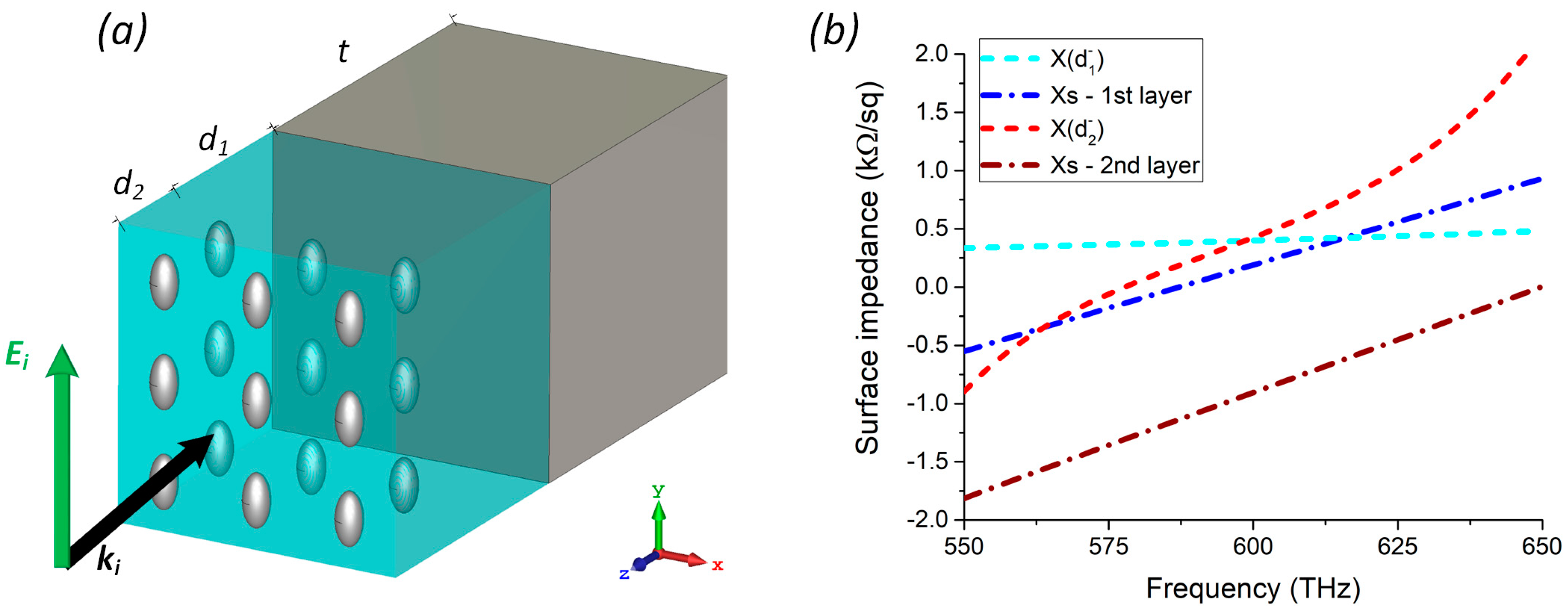
We start by considering the case of a CA absorber with
N = 2, whose structure is shown in
Figure 3a. The ideal infinitely-thin metallic ground plane shown in
Figure 1a is now replaced by a thick enough layer of silver (
t = 50 nm) that minimizes the transmission of light beyond the structure. We assume that the two nanoparticle arrays are placed on a silica layer, which is a non-magnetic material commonly used as a substrate for nanoparticles (
εd = 2.1). It is worth noticing that the choice of the dielectric substrate affects both the thickness of the absorber (equal to
λ/4 at the central frequency of operation) and the optimal size of the nanoparticles returned by the optimization process. Assuming a normal incidence, the reflection coefficient (6) reads as
where
kd is the wavenumber in silica,
Zs1 and
Zs2 are the complex surface impedances of the first and the second reactive layer, respectively, and
,
. It is important to underline that the first optical reactive layer is completely immersed in silica and, thus, the permittivity of the host medium to be used in (8) is the one of silica. Conversely, as it should be clear from
Figure 3a, the second reactive layer is placed between the dielectric and the vacuum. Thus, an average permittivity between these two dielectrics must be used as
εh.
The discrete frequency integral of the reflection coefficient (10) has been minimized under the described design constraints by assuming a central frequency
f = 600 THz and as minimum and maximum frequencies
fmin = 550 THz,
fmax = 650 THz, respectively. This leads to the following optimal parameters:
a1 =
a2 = 29 nm,
ry1 =
ry2 = 8 nm,
rx1 =
rx1 = 4 nm,
d1 = 55 nm,
d2 = 30 nm. It is important noticing that, even though the dimensions of the two nanoparticle arrays are the same, their surface reactance (shown in
Figure 3b) is different because of the different effective permittivity of their host material. In
Figure 3b, we also show the input reactance of the absorber evaluated at
and
, i.e., before the first and the second reactive layer, respectively. From this comparison, it should be clear that the optimization has led to reactive layers, whose surface reactance is engineered to compensate for the intrinsic dispersion of the dielectrics.
In
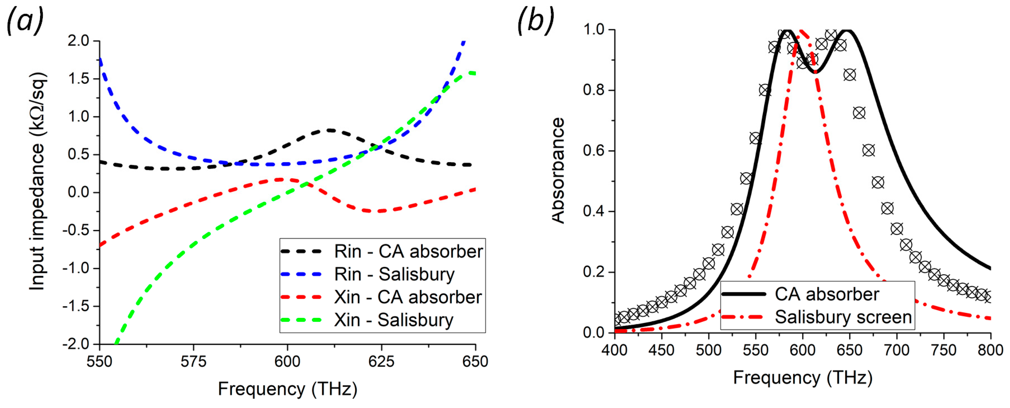
Figure 4a, we show the analytical real and imaginary parts of the overall input impedance
Zin at
z =
d1 +
d2. The input impedance is compared to the one of a single-layer optical Salisbury screen, whose resistive sheet is resonant and impedance-matched with the vacuum at 600 THz [
20]. As expected, the input reactance of the Salisbury screen is equal to zero only at a single frequency and increases quickly as we move away from the resonance. Conversely, the CA-absorber exhibits an input reactance that is close to zero within a wide range around the design frequency. This is confirmed by the results shown in
Figure 4b, where the absorbance of the two absorbers is compared. The CA absorber has a significantly broader absorption bandwidth due to the optimized reactive behavior of the lossy layers. Specifically, assuming an absorbance threshold of 0.9, the fractional bandwidth of the CA absorber is 13.2%, almost 4 times bigger than the one of the optical Salisbury screen. We stress that this comparison has been carried out by considering two absorbers with the same overall thickness.
The analytical absorbance of the CA absorber is compared to the one obtained through full-wave simulations carried out on a unit-cell of the CA absorber. As can be appreciated, there is a good agreement between the numerical and theoretical results, confirming the effectiveness of the method discussed in the previous Section. The agreement slightly deteriorates at higher frequencies mainly due to the progressive violation of the assumptions made to derive Equation (8) and to the non-perfect reflection of the backing silver layer. A possibility to reduce the transmittance of the absorber without increasing further its overall thickness could rely on the use of ultrathin optical mirrors based on dielectric nanoparticles [
38]. This would also make the design of broadband absorbers that are transparent outside their absorption bandwidth possible (similar to the narrowband design we have discussed in Reference [
21]).
We consider now the case of a CA absorber made by three layers (
N = 3). We apply the minimization procedure described above with the same design constraints and, in particular, by fixing the maximum thickness of the absorber equal to the one of the Salisbury screen. After a quick numerical optimization, we get the following optimum geometrical values:
a1 =
a2 =
a3 = 32 nm,
ry1 = 9 nm,
rx1 = 5 nm,
ry2 = 10 nm,
rx2 = 4 nm,
ry3 = 8 nm,
rx3 = 4 nm,
d1 = 40 nm,
d2 = 25 nm,
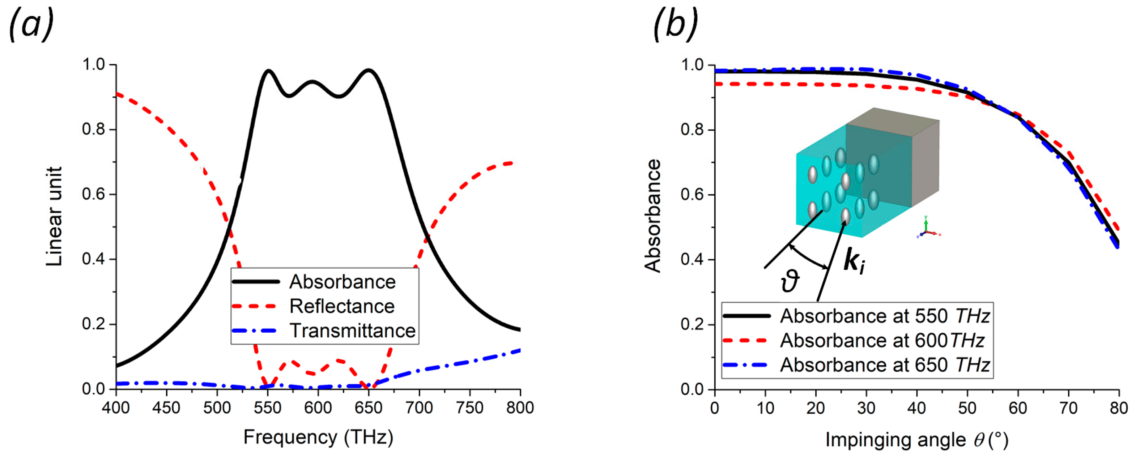
d3 = 25 nm. The reflectance, absorbance and transmittance of this absorber, obtained through full-wave simulations, are shown in
Figure 5a. As can be appreciated, the absorbance stays above 0.9 within the frequency range 540–670 THz, resulting in a fractional bandwidth bigger than 20% with a thickness of only
λ/4 at the center frequency of the absorption band. In
Figure 5b, we report the value of the absorbance at three different frequencies as the impinging angle
θ changes. As can be appreciated, for all the considered frequencies, the absorbance is larger than 0.9 for a wide range of incidence angles, up to 50°.
An interesting comparison between the Salisbury screen and the CA absorbers can be carried out by exploiting the metric defined by the Rozanov’s limit [
39]. Accordingly, the minimum thickness of a metal-backed absorber needed to achieve a reflectance
R(
λ) is equal to
Being theoretical bound, this parameter can be used to quantify univocally the performances of any grounded absorber. In particular, in our cases, the ratio between the actual thickness of the absorber and its theoretical minimum is equal to 8%, 21% and 28%, for the Salisbury screen and for the 2- and 3-layered CA absorber, respectively. Though the theoretical limit is still distant, mainly due to the strong dispersion of the nanoparticles-based optical metasurfaces, the improvement with respect to the Salisbury screen is significant.
Before concluding this Section, we would like to stress that the approach discussed in this manuscript to increase the absorption bandwidth of a Salisbury screen is inherently different from the one employed in the Jaumann absorber [
1]. The broadband absorption of a Jaumann screen, in fact, is achieved by stacking purely-resistive layers separated by different quarter-wavelength-thick dielectric layers. This approach significantly increases the overall thickness of the whole device. Conversely, CA absorbers exploit the additional degree of freedom provided by the reactive behavior of the lossy layers and allows for achieving wide absorption bandwidth without increasing the thickness of the Salisbury screen.
4. Alternative Layout and Sensitivity Analysis
The aim of this Section is to provide some interesting considerations about the geometry of the proposed absorbers in view of their possible experimental realization. For this purpose, (i) we propose an alternative geometry that may facilitate the experimental realization of the proposed CA-absorbers; (ii) we investigate its robustness towards some common inaccuracies that may arise during the nanofabrication process of the optical metasurfaces.
The first aspect we would like to discuss is the geometry of the nanoparticles composing the optical metasurfaces. In fact, the CA absorbers described in the previous Section require plasmonic ellipsoids, whose experimental realization, though possible, is not straightforward. However, as it should be clear from the discussion in
Section 2, the basic design principle of these devices relies on the control of the eccentricity and of the absolute size of nanoparticles. In other terms, their exact shape is not fundamental as far as it remains elongated. Therefore, we can replace the ellipsoids shown in
Figure 2a with nanocylinders that are much easier to be experimentally realized [
40,
41]. Unfortunately, a closed-form expression of the polarizability of finite-size cylinders is not known and, thus, we cannot extend Equation (8) to the case of an array of cylinders.
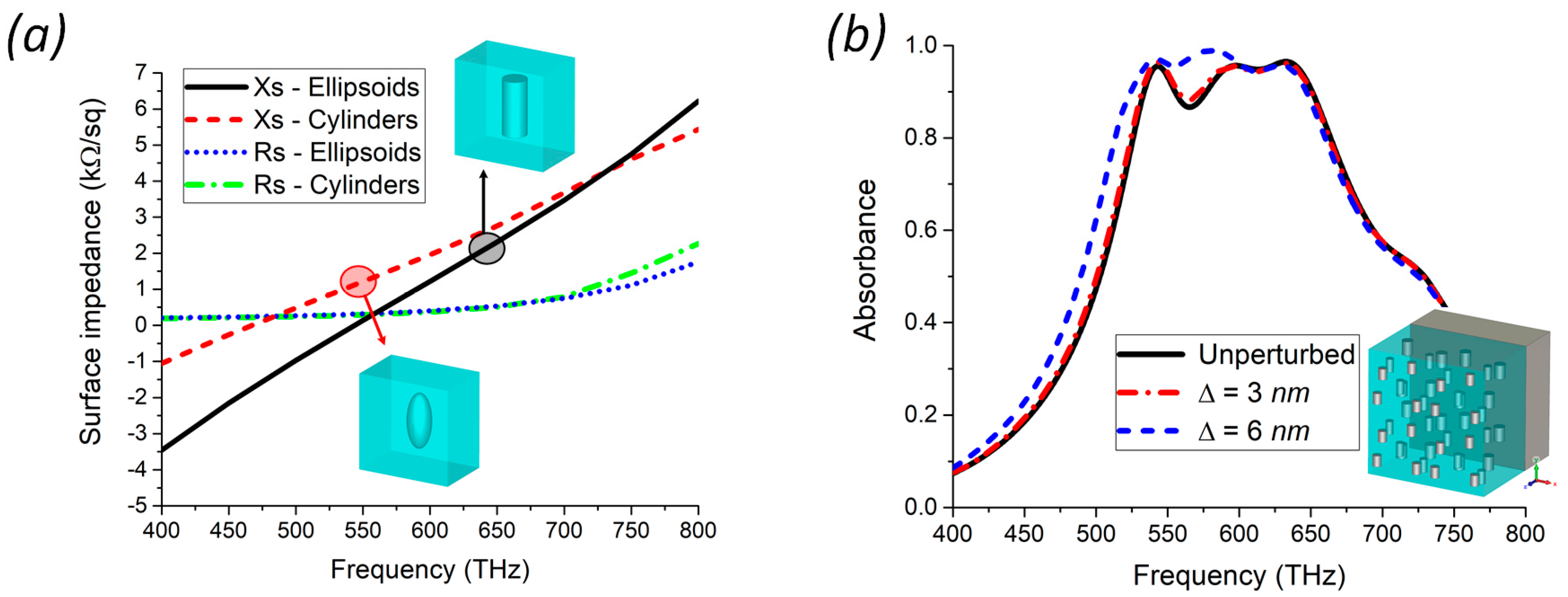
To overcome this issue, we need to numerically optimize the optical metasurfaces based on nanorods. For this purpose, in
Figure 6a we show the comparison between the complex surface impedance exhibited by the two optical metasurfaces made by ellipsoids and cylinders with the same linear dimensions embedded in a silica matrix. The values of the major and minor axes used for this example are the ones of the second layer of the three-layered CA absorber discussed in the previous section. As can be appreciated, the surface reactance is affected by the change of the shape, consistent with the discussion about their static polarizabilities available in [
42]. We need, thus, to re-optimize the size of the nanoparticles. Since the surface reactance mainly depends on the eccentricity, we may conveniently limit our optimization to the major axis of the cylinders. After some retrieval based on full-wave simulations, we get that a 30% reduction of the major axes allows for the restoration of the original surface reactance exhibited by the three layers. Please note that, in principle, these geometrical changes also affect the surface resistance of the metasurface. However, since we have only reduced the major axis without changing the minor ones, the variation of the surface resistance is negligible and does not significantly affect the performance of the absorber. This is confirmed by the full-wave absorbance of the nanocylinders-based CA absorber shown in
Figure 6b (black line).
The second important aspect we would like to investigate is the robustness of the device performances towards common manufacturing inaccuracies that may arise during the fabrication process. To this purpose, we have considered a square sample of the three-layered CA absorber made by 4 × 4 unit-cells. Each unit-cell is composed of three nanocylinders stacked along the
z-axis. In order to introduce a realistic perturbation, we have randomly divided the 48 cylinders into 6 groups. The elements of the first two groups have been translated along the
x-axis by a quantity ±Δ, respectively. Similarly, the elements of the third and fourth group have been moved along the
y-axis by a quantity ±Δ, respectively. Finally, the elements of the last two groups have been translated both along the
x- and the
y-axis by quantity ±Δ, respectively. The full-wave results for different values of Δ are shown in
Figure 6b. As can be appreciated, the response of the absorber is almost insensitive to the exact positions of the nanoparticles in the arrays. This is an expected result since, as described in
Section 2, the surface impedance of an optical metasurface is an average effect that does not depend on the exact position of the nanoparticles in the lattice. It is worth noticing that the proposed perturbation analysis is quite conservative since we have assumed that all nanoparticles are moved with respect to their original position of a quantity that is comparable to the length of their major axis.

