
Article

Characteristics and Influencing Factors of Multiplication Noise in EBCMOS


1
Science and Technology on Low-Light-Level Night Vision Laboratory, Xi’an 710065, China
2
School of Physics, Changchun University of Science and Technology, Changchun 130022, China
*
Author to whom correspondence should be addressed.
Photonics 2026, 13(6), 511; https://doi.org/10.3390/photonics13060511
Submission received: 29 April 2026 / Revised: 15 May 2026 / Accepted: 18 May 2026 / Published: 24 May 2026

Abstract

Based on the theory of photon propagation and the principle of electron–semiconductor interaction, this paper proposes a formation mechanism model of multiplication noise in the electron multiplication layer of EBCMOS. Using the Monte Carlo method, the signal-to-noise ratio (SNR) of multiplied electrons is calculated, and the effects of key structural design parameters (including the doping concentration of the P-type substrate, thickness of the electron multiplication layer, and the material and thickness of the passivation layer) along with the incident electron energy on multiplication noise are systematically analyzed. The results show that Al2O3 is the optimal passivation material for structural design, and the SNR can be effectively improved by increasing the incident electron energy, reducing the passivation layer thickness, decreasing the doping concentration, and thinning the electron multiplication layer. These findings provide theoretical insights for the electron multiplication layer structural optimization and performance improvement of EBCMOS.

1. Introduction

Electron-bombarded complementary metal–oxide–semiconductor (EBCMOS) has emerged as a novel optoelectronic imaging device engineered for ultra-low-light detection. Benefiting from its intrinsic advantages of high gain, compact architecture, light weight, low power consumption, and digital readout capability, EBCMOS exhibits substantial application potential in diverse fields, including low-light night vision, single-photon detection, and biological monitoring. Consequently, it presents a focal point of contemporary research in low-light imaging [1,2,3,4,5].
The signal-to-noise ratio (SNR) serves as the fundamental metric dictating the imaging performance of EBCMOS devices. The multiplication noise introduced during the electron bombardment multiplication process constitutes the primary bottleneck restricting SNR enhancement, representing a key unresolved issue in current low-light imaging research. Previous studies by Hirvonen et al. revealed that the multiplication noise, modified by the Fano factor, is the principal source of intrinsic multiplication noise in such devices, with its statistical fluctuations directly determining the theoretical limit of the SNR [6]. Furthermore, He et al. elucidated that dark-current noise, dominated by interface defects, and gain fluctuations during the electron multiplication process represent the two critical factors constraining noise performance [7]. A noise suppression and edge enhancement algorithm based on a field programmable gate array developed by Cao et al. demonstrated peak SNR improvements of 11.37% and 26.64% compared to standard median and Gaussian filtering, respectively, significantly improving the noise suppression effect and edge detail retention ability of images [8]. For the mixed noise present in EBCMOS images, a self-supervised two-stage denoising algorithm is proposed by Li et al., demonstrating that multiplication noise typically manifests as oversaturated, patch-like pixel clusters [9]. Additionally, the precise detection and elimination of multiplication noise utilizing a Harris corner detection approach were achieved by Zhao et al., resulting in a substantial improvement in imaging quality [10]. Wang et al. established a statistical model of the grayscale distribution of flicker noise under varying bombardment voltages and developed a corresponding denoising algorithm, enabling pixel-level accurate localization and elimination of flicker noise [11]. Liu et al. proposed a noise reduction algorithm based on the noise characteristics of EBCMOS images, which effectively suppresses multiple types of noise in EBCMOS devices, significantly restores image edge details, and achieves comprehensive improvement of image quality in low-light environments [12]. Despite these algorithmic advancements, the overwhelming majority of existing studies remain focused on the algorithmic suppression of image degradation caused by multiplication noise, or on the phenomenological description and qualitative analysis of multiplication noise generation. A systematic theoretical model of multiplication noise during the electron bombardment multiplication process, as well as the physical mechanisms by which device structural parameters dictate this noise, is hitherto lacking.
In this paper, a theoretical calculation model for the multiplication noise and SNR in EBCMOS is established based on the principles of semiconductor materials and the Monte Carlo method. In addition, an in-depth theoretical analysis is conducted to examine the influence of structural design parameters, including passivation layer material selection, incident electron energy, passivation layer thickness, doping concentration, and electron multiplication layer thickness, on the multiplication noise in the electron multiplication layer of EBCMOS devices. The research results presented herein provide a solid theoretical foundation for noise testing experiments and the fabrication of prototype devices for EBCMOS.

2. Theoretical Model

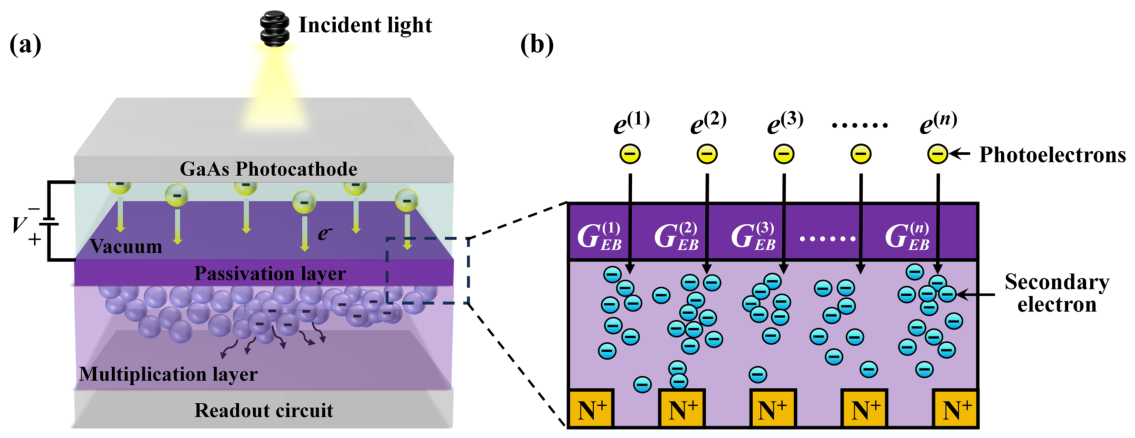
In order to analyze the properties of multiplication noise in the multiplication layer of EBCMOS, it is necessary to introduce the principle of the device. Figure 1a shows a schematic diagram of the structure of EBCMOS. Here, under the action of the GaAs photocathode, incoming light from the external environment is converted into photoelectrons, which are then accelerated to obtain high energies by the voltage applied between the photocathode and CMOS anode, resulting in electron bombardment into the passivation and multiplication layers. An electron bombardment semiconductor (EBS) gain is formed due to the generation of a large number of electron–hole pairs in the above process [13]. However, when high-energy photoelectrons strike the surface of the semiconductor, the resulting multiplied electrons may have random energies and directions, resulting in the spreading of the charge distribution and gain fluctuations in different regions [14]. Figure 1b shows a magnified view of the electron bombardment process in the electron multiplication layer.
Due to the randomness of the electron multiplication process, each electron is amplified by an individual gain factor, resulting in an uncertain total charge gain. However, the average gain G can be determined. The calculation formula for the average gain is given by [15]
G = ε E E d e a d w
where ε is the charge collection efficiency (CCE); E is the energy of the incident photoelectron; E d e a d is the energy lost by the electron as it passes through the passivation layer; and w is the energy consumed to produce an electron–hole pair for the incident electron. For silicon (Si) materials, the value of w is 3.6 eV [16].
As the incident electrons move into the CMOS image sensor chip, their motion follows a random pattern, and the state of motion in the multiplication layer cannot be determined directly. Therefore, the Monte Carlo method is used to simulate the movement of electrons within the CMOS image sensor chip [17]. When electrons bombard the passivation layer on the surface of the CMOS, elastic and inelastic scattering can occur due to the interaction between electrons and the solid material. Elastic scattering requires consideration of the directional changes that affect the electron’s trajectory, while inelastic scattering requires consideration of the energy loss of the electron during the collision process. The passivation layer typically contains two types of atoms, and Monte Carlo sampling methods can be used to distinguish between the atoms that interact with the electrons. The probability of electron collisions with each type of atom can be calculated using the total scattering cross-section per unit volume. This allows for the calculation of the remaining energy of the electron after the y-th scattering event, which can be expressed as
E y + 1 = E y d E d s | E y · Δ y
where Δ y represents the scattering step length after the y-th electron scattering event, E y is the remaining energy of the electron after the y-th scattering, and d E / d s is the stopping power (SP), also known as the energy loss rate. For the stopping power, our research group used a fitting function for the SP equation [18]:
d E d s = F ( Z ) G ( E ) λ i n = ( A Z + B ) ( C ln E + D ) λ i n = c 1 ( c 2 Z + 1 ) ln ( c 3 E ) λ i n
where λ i n is the mean free path for inelastic scattering, Z is the atomic number, and E is the energy of the incident electron. The functions F ( Z ) = A Z + B , G ( E ) = C l n E + D describe the relationships between the atomic number and the stopping power and between the electron energy and the inelastic scattering mean free path, respectively. The parameters A , B , C , and D are constants that are independent of energy and atomic number, and they are determined through fitting the curves of electron energy versus stopping power and inelastic scattering mean free path for 27 different elements. These parameters are calculated as follows: c 1 = B C , c 2 = A / B , c 3 = e x p ( D / C ) .
After electron multiplication, multiplied electrons undergo diffusion due to the concentration gradient in the P-type substrate. The diffusion process of the multiplied electron can be viewed as the injection of steady-state nonequilibrium carriers. The diffusion velocity of the electrons v d can be expressed as [19]
v d = ( D y r + D y L y )
In the formula, D y is the electron diffusion coefficient, L y = ( D y · τ y ) 1 / 2 is the diffusion length, r is the distance of the electron from the diffusion center, and τ y is the minority carrier lifetime.
Based on the Einstein relation, the relationship between the diffusion coefficient and the mobility μ y can be expressed as
D y μ y = k T q
where q is the charge of the electron, k is the Boltzmann constant, and T is the thermodynamic temperature.
During the diffusion process, electrons may undergo recombination. Therefore, the actual number of electrons collected must account for the electrons that have recombined and been lost. The number of collected electrons can be expressed as
N c o l l e c t = N i j · [ e t 1 τ 1 e t i τ i e t m τ m ]
where N i j is the total number of initially generated electrons, and t i is the transit time of electrons during the diffusion process.
The charge collection efficiency ε is defined as the ratio of the number of collected electrons N c o l l e c t to the total number of multiplied electrons N m u l t i p l y :
ε = N c o l l e c t N m u l t i p l y
Assuming that N initial electrons are incident on the CMOS passivation layer, each electron is amplified by the gain factor G ( i ) . The total output signal S o u t can be expressed as the sum of all the electrons amplified by the gain:
S o u t = i N G ( i )
The mean of the output signal can be calculated using the expected value of the gain factor for each electron, while the variance of the output signal reflects the fluctuation of the signal. The average value and variance of the output signal are as follows:
μ S o u t = N G
ν S o u t = N ( G 2 + σ G 2 )
where σ G 2 represents the variance of the EBS gain process with average single-photon electron gain, which describes the degree of gain fluctuations and is typically used to characterize the magnitude of multiplication noise by quantifying the variance of these fluctuations [20,21,22].
In EBCMOS, the point spread function (PSF) significantly influences the noise characteristics [23,24,25]. When electrons bombard the backside of the CMOS sensor, numerous multiplied electrons are generated. These multiplied electrons then diffuse towards the photodiodes within the pixels, resulting in some spatial separation. This spatial separation disperses the noise across several pixels, reducing the noise that each individual pixel experiences. This effect impacts the variance of the electron multiplication stage, thereby resulting in the total measured noise being lower than that under other conditions. To account for this effect, the correction factor β is introduced, which considers the influence of the PSF on the noise distribution [26]. This factor helps to more accurately reflect the actual noise characteristics. The corrected variance of the output signal, taking into account the spatial diffusion of the noise, can be represented by the following equation for the standard deviation σ and pixel width p:
β ( p , σ ) = [ e r f p 2 σ 1 π 2 σ p ( 1 e p 2 σ 2 ) ] 2
The corrected variance, after considering the point spread function (PSF) and the correction factor β , can be expressed as
σ S o u t 2 = β ( G 2 N + N σ G 2 )
The final SNR of the electron multiplication layer in EBCMOS can be expressed as
S N R = N β ( 1 + σ G 2 G 2 )

3. Results and Discussion

Owing to the randomness inherent in electron motion, this paper employs the Monte Carlo method, which is capable of analyzing the motion of a large number of electrons, and combines it with the aforementioned theoretical model to conduct an in-depth analysis of the influence of structural parameters (including passivation layer materials, incident electron energy, passivation layer thickness, doping concentration, and electron multiplication layer thickness) on the multiplication noise of the electron multiplication layer in EBCMOS.

3.1. Influence of Passivation Layer Material on SNR

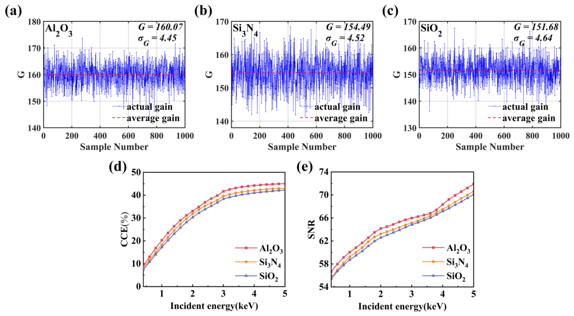
Firstly, the influence of passivation layer materials on the SNR is analyzed, and gain fluctuations and the variations in CCE and SNR with incident electron energy under different passivation layer materials are simulated, as shown in Figure 2, under the simulation conditions of a light intensity of 0.01 lx, a photocathode conversion efficiency of 25%, an incident electron diameter of 10 nm, a pixel size of 10 µm × 10 µm, a passivation layer thickness of 10 nm, a P-type substrate doping concentration of 1015 cm−3, an electron multiplication layer thickness of 10 µm, and an operating temperature of 300 K.
Figure 2a–c illustrate the influences of three passivation layer materials—Al2O3, Si3N4 and SiO2—on the average gain G and the standard deviation of gain fluctuation σ G of the electron multiplication layer in EBCMOS under an incident electron energy of 2 keV, where blue data points represent the gain values obtained from multiple simulation measurements and the red dashed lines denote the average gain for each material. The results show that the values of G for Al2O3, Si3N4, and SiO2 are 160.07, 154.49, and 151.68, respectively, with corresponding σ G values of 4.45, 4.52, and 4.64 at 2 keV incident electron energy. Notably, the Al2O3 passivation layer exhibits a higher average gain and lower gain fluctuation than Si3N4 and SiO2. This is because the higher-density Al2O3 features a more compact atomic arrangement, which reduces the interface state density, significantly decreasing the probability of electron recombination at the surface and thus enhancing the average gain. Simultaneously, the reduction in recombination effects suppresses the randomness of the multiplication process, minimizing the amplitude of gain fluctuations and thereby reducing the excess noise introduced by gain variations. Figure 2d,e further illustrate the trends of CCE and SNR as functions of incident electron energy under different passivation layer materials. It can be seen that CCE gradually increases with increasing incident electron energy, rising rapidly when the energy is below 2 keV, slowing down after exceeding 2 keV, and tending to stabilize at around 3 keV. Similarly, SNR also improves with increasing incident electron energy, growing rapidly below 2 keV and slowing down thereafter. Additionally, Al2O3 exhibits the optimal CCE and SNR at the same incident electron energy, which is attributed to the fact that low-energy incident electrons suffer significant energy loss in the passivation layer, leading to low CCE and reduced SNR due to the randomness of energy loss exacerbating gain fluctuations. As the incident electron energy increases, energy loss in the passivation layer decreases, allowing more electrons to undergo multiplication, which increases the concentration in the diffusion region, thereby enhancing CCE and the average gain of the electron multiplication layer. Higher incident electron energy also improves the stability of the multiplication process, reducing gain fluctuations and ultimately boosting SNR. Among the three passivation layer materials, Al2O3 exhibits high density, low electron stopping power, and superior interfacial passivation capability, not only effectively mitigating the incident electron energy loss within the passivation layer but also suppressing interfacial charge recombination, thereby enabling the device to maintain consistently high CCE and SNR. Consequently, adopting Al2O3 as the passivation layer represents an effective strategy for enhancing device CCE and SNR in the design of EBCMOS devices.

3.2. Influence of Passivation Layer Thickness on SNR

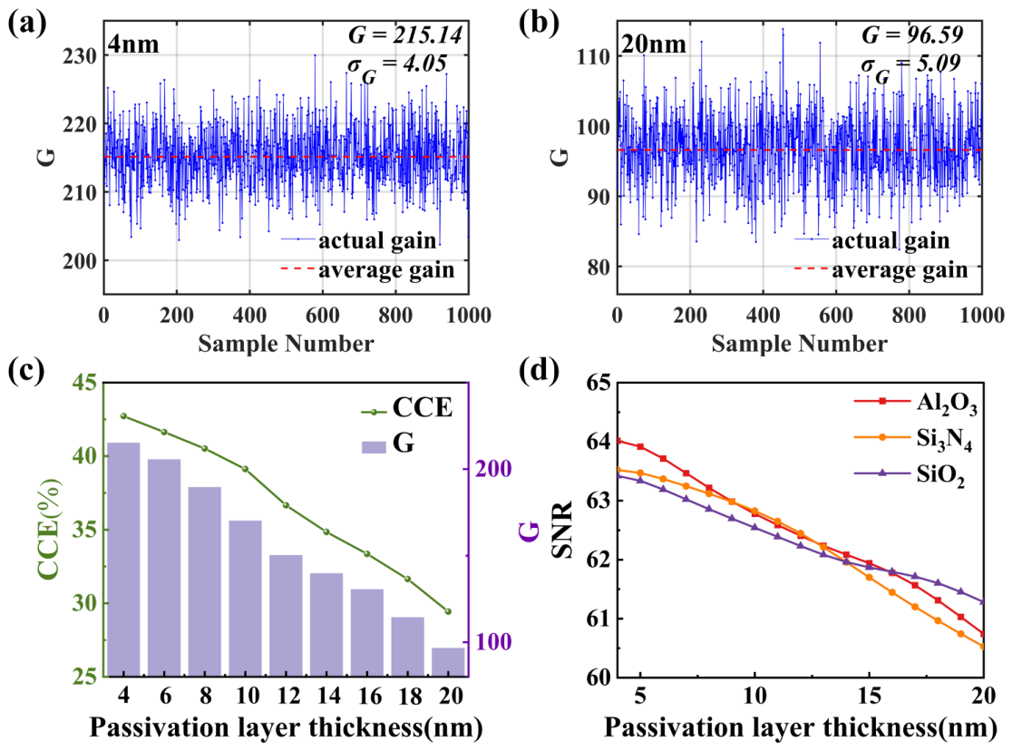
Next, the influence of passivation layer thickness on the SNR is analyzed, and the gain fluctuations and the variations in CCE, G, and SNR with passivation layer thickness are simulated under simulation conditions of a light intensity of 0.01 lx, a photocathode conversion efficiency of 25%, an incident electron energy of 2 keV, an incident electron diameter of 10 nm, a pixel size of 10 µm × 10 µm, a P-type substrate doping concentration of 1015 cm−3, an electron multiplication layer thickness of 10 µm, and an operating temperature of 300 K, as shown in Figure 3.
As shown in Figure 3a,b, when the Al2O3 passivation layer thickness is 4 nm and 20 nm, the corresponding average gains of the EBCMOS devices are 215.14 and 96.59, with standard deviations of gain fluctuations being 4.05 and 5.09, respectively. This indicates that increasing the passivation layer thickness reduces the electron multiplication efficiency and overall gain by prolonging the scattering path of incident electrons, thereby increasing the probability of inelastic collisions between electrons and atoms, while the scattering process makes the energy distribution of electrons reaching the multiplication layer more discrete, amplifying the statistical fluctuations in the multiplication process and thus intensifying gain fluctuations. Figure 3c further reveals the trends of CCE and G with the Al2O3 passivation layer thickness, showing that both exhibit a downward trend as the thickness increases. Thicker passivation layers not only increase energy loss during electron transport but may also cause some electrons to deviate from the multiplication region due to scattering, thereby reducing CCE and further decreasing the average gain. Figure 3d presents the evolution trend of SNR with passivation layer thickness for three passivation materials (Al2O3, Si3N4, and SiO2), demonstrating that SNR decreases as the thickness increases because signal strength reduces due to gain attenuation, while increased gain fluctuations introduce additional excess noise, leading to a decline in the SNR. Therefore, increasing the passivation layer thickness prolongs the electron scattering path, exacerbates energy loss, and amplifies statistical fluctuations in the multiplication process, thereby reducing the average gain, CCE, and SNR of EBCMOS devices. Thus, thinning the passivation layer thickness can effectively suppress the multiplication noise in EBCMOS and optimize the SNR.

3.3. Influence of Doping Concentration on SNR

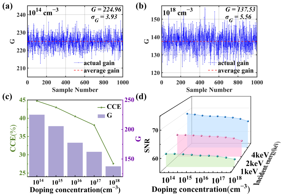
Then, the influence of the uniform doping concentration of the P-type substrate on the SNR is analyzed, and the gain fluctuations and variations in CCE, G, and SNR with the doping concentration are simulated under the simulation conditions of a light intensity of 0.01 lx, a photocathode conversion efficiency of 25%, an incident electron energy of 2 keV, an incident electron diameter of 10 nm, a pixel size of 10 µm × 10 µm, a passivation layer material of Al2O3 with a thickness of 4 nm, an electron multiplication layer thickness of 10 µm, and an operating temperature of 300 K, as shown in Figure 4.
Figure 4a,b show gain fluctuation when the doping concentration of the P-type substrate is 1014 cm−3 and 1018 cm−3, respectively. It can be seen that, as the doping concentration increases, the gain fluctuation significantly intensifies with σ G increasing from 3.93 to 5.56; this phenomenon arises because excessively high doping concentration significantly increases the density of carrier recombination centers in the material, making electrons more prone to recombination during the multiplication process, which not only reduces the gain but also amplifies the statistical fluctuations of the multiplication process through the randomness of the recombination process, thus significantly increasing the amplitude of gain fluctuation. Figure 4c further demonstrates the variation trends of charge collection efficiency and average gain with different doping concentrations: when the doping concentration increases from 1014 cm−3 to 1018 cm−3, both the charge collection efficiency and the average gain of the electron multiplication layer show a downward trend, with the decline rate accelerating significantly in the range of 1017 cm−3 to 1018 cm−3. Figure 4d simulates the trend of SNR changing with doping concentration under different incident electron energies, showing that SNR gradually decreases as the doping concentration increases. When the doping concentration increases from 1014 cm−3 to 1015 cm−3, the SNR decreases slightly. Meanwhile, continuing to increase the doping concentration leads to a significantly accelerated SNR decline rate. The influence of doping concentration on SNR strengthens with the increase in incident electron energy. Specifically, when the doping concentration increases from 1014 cm−3 to 1018 cm−3, the SNR value decreases from 59.79 to 57.83 (a decrease of 3.3%) at an incident electron energy of 1 keV, from 63.49 to 61.20 (a decrease of 3.6%) at 2 keV, and from 68.95 to 65.84 (a decrease of 4.5%) at 4 keV. The fundamental reason for this phenomenon is that high doping concentration significantly increases the density of carrier recombination centers, causing part of the electrons to be recombined before completing the multiplication process, thereby reducing the charge collection efficiency and average gain; additionally, the randomness of the recombination process exacerbates gain fluctuations and introduces more multiplication noise, leading to a decrease in the SNR. Therefore, controlling the doping concentration of the P-type substrate within 1015 cm−3 can effectively suppress carrier recombination, thereby enhancing electron multiplication efficiency, reducing gain fluctuations, and ultimately achieving high gain and high SNR for EBCMOS devices. Therefore, a doping concentration of 1014 cm−3 was adopted for the P-type substrate in all subsequent simulations.

3.4. Influence of Electron Multiplication Layer Thickness on SNR

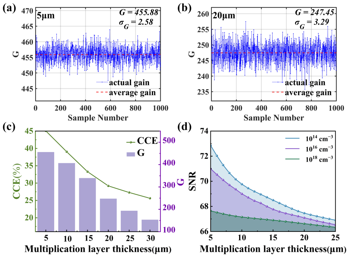
Subsequently, the influence of the thickness of the electron multiplication layer on the SNR is analyzed, and the gain fluctuations and the variations in CCE, G, and SNR with different electron multiplication layer thicknesses are simulated, as shown in Figure 5. The simulation conditions are as follows: a light intensity of 0.01 lx, a photocathode conversion efficiency of 25%, an incident electron energy of 4 keV, an incident electron diameter of 10 nm, a pixel size of 10 µm × 10 µm, a passivation layer material of Al2O3, a passivation layer thickness of 4 nm, a P-type substrate doping concentration of 1014 cm−3, and an operating temperature of 300 K.
Figure 5a,b show gain fluctuation when the thickness of the electron multiplication layer is 5 µm and 20 µm, respectively. As the thickness of the electron multiplication layer increases, the average gain exhibits a downward trend while the gain fluctuation gradually intensifies. This phenomenon is primarily attributed to the fact that increasing the thickness of the electron multiplication layer directly prolongs the propagation path of electrons within the multiplication layer. When electrons traverse a thicker multiplication layer, they undergo more inelastic scattering with atoms, leading to intensified electron energy loss and thus a decrease in overall gain. Simultaneously, the randomness of the scattering process makes the energy distribution of electrons in the multiplication layer more discrete, amplifying the statistical fluctuations of the multiplication process and ultimately resulting in enhanced gain fluctuations. Figure 5c further demonstrates the variation trends of charge collection efficiency and average gain with the thickness of the electron multiplication layer, indicating that both the charge collection efficiency and gain show a downward trend: specifically, when the thickness of the electron multiplication layer increases from 5 µm to 30 µm, the charge collection efficiency decreases from 45.05% to 25.63%, and the gain decreases from 455.88 to 153.29. Figure 5d simulates the changes in SNR under different doping concentrations (1014 cm−3, 1016 cm−3, and 1018 cm−3) as the thickness of the electron multiplication layer varies, showing that the SNR at each concentration gradually decreases with the increase in electron multiplication layer thickness; when the thickness increases from 5 µm to 10 µm, the SNR decreases rapidly, while when the thickness further increases, the SNR decline rate gradually slows down and eventually tends to be gentle. The reason for this phenomenon is that an excessively thick electron multiplication layer increases the recombination probability of electrons during transport as the thickness increases, reducing the number of effective electrons participating in multiplication and thus decreasing the charge collection efficiency and gain, which directly weakens the signal strength; meanwhile, the intensified statistical fluctuations of the multiplication process increase the multiplication noise, further reducing the SNR. Therefore, it is necessary to minimize the thickness of the electron multiplication layer as much as possible to suppress recombination loss and gain fluctuations, thereby improving the SNR of the device.

4. Conclusions

In this paper, a detailed theoretical model of multiplication noise for the electron multiplication layer in EBCMOS devices was established using the Monte Carlo method, and a comprehensive analysis was conducted on the influence of the internal structural parameters of EBCMOS devices on their SNR performance. Firstly, the passivation layer material has a significant impact on the SNR. By selecting appropriate passivation materials and optimizing their thickness, both the SNR and the gain of the device can be effectively improved. The simulation results show that the Al2O3 passivation layer performs best under high-SNR conditions, while Si3N4 and SiO2 are comparatively inferior. Secondly, by optimizing the structural design and adopting measures such as reducing the thickness of the passivation layer, controlling the doping concentration of the P-type substrate at a relatively low level, and reducing the thickness of the electron multiplication layer, the generation of multiplication noise can be effectively suppressed, thus improving the SNR of the device. Based on these simulation results, the structural design of EBCMOS devices can be optimized to achieve optimal performance for specific applications. In summary, to obtain an EBCMOS device with a high SNR, the following structural design is recommended: an incident electron energy of 4 keV, an incident electron diameter of 10 nm, a passivation layer material of Al2O3, a passivation layer thickness of 4 nm, an electron multiplication layer thickness of 5 µm, and a P-type substrate doping concentration of 1015 cm−3, which yields an SNR of up to 70.95 dB. The research results presented in this study provide theoretical support for the development of high-SNR imaging devices and lay a solid foundation for the structural design of future high-performance imaging systems.

Author Contributions

Conceptualization, G.J. and W.C.; methodology, C.W. and R.L.; software, R.L. and Y.L. (Yuanhe Liu); validation, L.Y., D.S. and Y.L. (Ye Li); formal analysis, C.W. and R.L.; investigation, G.J.; resources, W.C.; data curation, W.C.; writing—original draft preparation, G.J.; writing—review and editing, W.C., D.S. and Y.L. (Ye Li); visualization, C.W.; supervision, L.Y. and Y.L. (Ye Li); project administration, W.C. All authors have read and agreed to the published version of the manuscript.

Funding

This research was funded by the Key Laboratory Fund (J20220103), the National Natural Science Foundation of China (Grant Nos. U2141239, U2031113, and 12274041), and the Construction of Independent Innovation Capability for the Jilin Provincial Engineering Research Center of Optoelectronic Detection and Multidimensional Information Processing (2021C032).

Data Availability Statement

The data that support the findings of this study are available from the corresponding author upon reasonable request.

Conflicts of Interest

The authors declare no conflicts of interest.

References

  1. Cajgfinger, T.; Dominjon, A.; Barbier, R. Single photon detection and localization accuracy with an ebCMOS camera. Nucl. Instrum. Methods Phys. Res. Sect. A 2015, 787, 176–181. [Google Scholar] [CrossRef]
  2. Zhang, J.; Qian, Y.; Zhang, Y.; Jiao, G.; Liu, J. High-Resolution Low-Light Electron-Bombarded Active Pixel Sensor with a Fully Frontside-Thinned Structure and Its Noise Characteristics. IEEE Trans. Electron Devices 2025, 72, 3680–3690. [Google Scholar] [CrossRef]
  3. Dominjon, A.; Ageron, M.; Barbier, R.; Billault, M.; Brunner, J.; Cajgfinger, T.; Calabria, P.; Chabanat, E.; Chaize, D.; Doan, Q.; et al. An ebCMOS camera system for marine bioluminescence observation: The LuSEApher prototype. Nucl. Instrum. Methods Phys. Res. Sect. A 2012, 695, 172–178. [Google Scholar] [CrossRef]
  4. Barbier, R.; Cajgfinger, T.; Calabria, P.; Chabanat, E.; Chaize, D.; Depasse, P.; Doan, Q.; Dominjon, A.; Guérin, C.; Houles, J.; et al. A single-photon sensitive ebCMOS camera: The LUSIPHER prototype. Nucl. Instrum. Methods Phys. Res. Sect. A 2011, 648, 266–274. [Google Scholar] [CrossRef]
  5. Wang, X.; Song, D.; Jiao, G.; Li, Y.; Chen, W. Characterising Backscattered Electrons in EBCMOS. IEEE Photonics J. 2022, 14, 6858605. [Google Scholar] [CrossRef]
  6. Hirvonen, L.; Suhling, K. Photon Counting Imaging with an Electron-Bombarded Pixel Image Sensor. Sensors 2016, 16, 617. [Google Scholar] [CrossRef] [PubMed]
  7. He, X.; Jiao, G.; Cheng, H.; Lu, T.; Li, Y.; Song, D.; Chen, W. Influencing factors of noise characteristics in EBCMOS with uniformly doped P-type substrates. J. Semicond. 2026, 47, 012302. [Google Scholar] [CrossRef]
  8. Cao, Y.; Zhu, X.; Zhang, X.; Zhao, W.; Ma, J. Noise Image Processing Algorithm for a Low-light EBCMOS Acquisition System Based on FPGA. Acta Photonica Sin. 2024, 53, 1110002. [Google Scholar]
  9. Li, B.; Liu, X.; Zhao, Z.; Li, L.; Jin, W. Self-Supervised Two-Stage Denoising Algorithm Based on Blind-Spot Network for EBAPS Images. Acta Opt. Sin. 2024, 44, 2210001. [Google Scholar]
  10. Zhao, Z.; Li, B.; Lian, T.; Liu, X.; Li, L.; Yan, L. Fast Denoising Algorithm for EBAPS Images Based on Harris Corner Detection. Acta Opt. Sin. 2025, 45, 1510006. [Google Scholar]
  11. Wang, Y.; Ding, Z.; Liu, J.; Wang, H.; Qian, Y. Adaptive denoising method for EBAPS images captured under ultra-low-light conditions via scintillation noise detection and region-specific filtering. Opt. Express 2025, 33, 35238–35256. [Google Scholar] [CrossRef]
  12. Liu, X.; Li, R.; Jin, W.; Li, L.; Yan, L.; Lei, S. Total variational noise reduction method for EBAPS image based on weighted nuclear norm minimization. Opt. Express 2025, 33, 1932–1951. [Google Scholar] [CrossRef] [PubMed]
  13. Meijer, E.; Leeuw, D.; Setayesh, S.; Veenendaal, E.; Huisman, B.; Blom, P.; Hummelen, J.; Scherf, U.; Klapwijk, T. Solution-processed ambipolar organic field-effect transistors and inverters. Nat. Mater. 2003, 2, 678–682. [Google Scholar] [CrossRef] [PubMed]
  14. Bai, J.; Bai, Y.; Hou, X.; Cao, W.; Yang, Y.; Wang, B.; Bai, X.; Li, S. The analysis of electron scattering among multiplying layer in EBAPS using optimized Monte Carlo method. Mod. Phys. Lett. B 2020, 34, 2050398. [Google Scholar] [CrossRef]
  15. Hirvonen, L.; Jiggins, S.; Sergent, N.; Zanda, G.; Suhling, K. Photon counting imaging with an electron-bombarded CCD: Towards wide-field time-correlated single photon counting (TCSPC). Nucl. Instrum. Methods Phys. Res. Sect. A 2015, 787, 323–327. [Google Scholar] [CrossRef]
  16. Fiebiger, J.; Muller, R. Pair-Production Energies in Silicon and Germanium Bombarded with Low-Energy Electrons. J. Appl. Phys. 1972, 43, 3202–3207. [Google Scholar] [CrossRef]
  17. Shimizu, R.; Kataoka, Y.; Ikuta, T.; Koshikawa, T.; Hashimoto, H. A Monte Carlo approach to the direct simulation of electron penetration in solids. J. Phys. D Appl. Phys. 1976, 9, 101. [Google Scholar] [CrossRef]
  18. Chen, W.; Chen, W.; Song, D.; Zhao, P.; Li, Y.; Li, S.; Wang, C.; Liang, R.; Yue, J. A universal gain theory of the multiplying layer in EBCMOS based on elastic and inelastic scattering. Nucl. Instrum. Methods Phys. Res. Sect. B 2024, 551, 165352. [Google Scholar] [CrossRef]
  19. Zhao, Y.; Meng, X.; Peng, S.; Miao, G.; Gao, Y.; Peng, B.; Cui, W.; Hu, Z. Physical mechanism of secondary-electron emission in Si wafers. Chin. Phys. B 2024, 33, 047901. [Google Scholar] [CrossRef]
  20. Feng, C.; Zhang, Y.; Qian, Y.; Liu, J.; Zhang, J.; Zhang, J.; Shi, F.; Bai, X.; Zou, J. Improved quantum efficiency and stability of GaAs photocathode using favorable illumination during activation. Ultramicroscopy 2019, 202, 128–132. [Google Scholar] [CrossRef] [PubMed]
  21. Zhang, Y.; Lu, X.; Wang, G.; Hu, Y.; Xu, J. Modeling random telegraph signal noise in CMOS image sensor under low light based on binomial distribution. Chin. Phys. B 2016, 25, 070503. [Google Scholar] [CrossRef]
  22. Lowe, B. Measurements of Fano factors in silicon and germanium in the low-energy X-ray region. Nucl. Instrum. Methods Phys. Res. Sect. A 1997, 399, 354–364. [Google Scholar] [CrossRef]
  23. Miora, R.; Rohwer, E.; Kielhorn, M.; Sheppard, C.; Bosman, G.; Heintzmann, R. Calculating point spread functions: Methods, pitfalls, and solutions. Opt. Express 2024, 32, 27278–27302. [Google Scholar] [CrossRef] [PubMed]
  24. Freitas, L.; Morgado-Dias, F. Design Improvements on Fast, High-Order, Incremental Sigma-Delta ADCs for Low-Noise Stacked CMOS Image Sensors. Electronics 2021, 10, 1936. [Google Scholar] [CrossRef]
  25. Zhang, Y.; Zheng, J.; Zhao, J.; Jiao, G.; Song, D.; Zhao, P.; Chen, W. Factors Influencing Spatial Resolution in EBCMOS Devices Under Substrate Bulk Gradient Doping. IEEE Trans. Electron Devices 2026, 73, 925–929. [Google Scholar] [CrossRef]
  26. Werner, F.; Veith, B.; Zielke, D.; Kühnemund, L.; Tegenkamp, C.; Seibt, M.; Brendel, R.; Schmidt, J. Electronic and chemical properties of the c-Si/Al2O3 interface. J. Appl. Phys. 2011, 109, 113701. [Google Scholar] [CrossRef]
Figure 1. (a) Principle diagram of EBCMOS. (b) Schematic diagram of the electron bombardment electron multiplication layer.
Photonics 13 00511 g001
Figure 2. The influence of passivation layer materials on multiplication noise: the gain fluctuations when the passivation layer materials are (a) Al2O3, (b) Si3N4, and (c) SiO2. (d) The variation of CCE with incident electron energy under different passivation layer materials. (e) The change of SNR as a function of incident electron energy for various passivation layer materials.
Photonics 13 00511 g002
Figure 3. The influence of passivation layer thickness on multiplication noise: the gain fluctuations when the passivation layer thicknesses are (a) 4 nm and (b) 20 nm. (c) The variations in CCE and G with passivation layer thickness for the Al2O3 passivation layer. (d) The changes in SNR as a function of passivation layer thickness for various passivation layer materials.
Photonics 13 00511 g003
Figure 4. The effect of doping concentration on multiplication noise: the gain fluctuations at doping concentrations of (a) 1014 cm−3 and (b) 1018 cm−3. (c) The variations in CCE and G with doping concentration at an incident electron energy of 2 keV. (d) The changes in SNR as a function of doping concentration for various incident electron energies.
Photonics 13 00511 g004
Figure 5. The effect of electron multiplication layer thickness on multiplication noise: the gain fluctuations for electron multiplication layer thicknesses of (a) 5 µm and (b) 20 µm. (c) The variations in CCE and G with electron multiplication layer thickness. (d) The changes in SNR as a function of electron multiplication layer thickness for different doping concentrations.
Photonics 13 00511 g005
Disclaimer/Publisher’s Note: The statements, opinions and data contained in all publications are solely those of the individual author(s) and contributor(s) and not of MDPI and/or the editor(s). MDPI and/or the editor(s) disclaim responsibility for any injury to people or property resulting from any ideas, methods, instructions or products referred to in the content.