
Article

Proposal of Compact Photonic Quantization Based on Dual-Output Mach-Zehnder Modulators


School of Communication Engineering, Hangzhou Dianzi University, Xiasha, Hangzhou 310018, China
*
Author to whom correspondence should be addressed.
Photonics 2026, 13(5), 461; https://doi.org/10.3390/photonics13050461
Submission received: 16 April 2026 / Revised: 28 April 2026 / Accepted: 29 April 2026 / Published: 7 May 2026
(This article belongs to the Special Issue Microwave Photonics: Advances and Applications)

Abstract

In this paper, to reduce system complexity and improve performance, we propose a novel compact photonic quantization scheme based on dual-output Mach–Zehnder modulators (DOMZMs). By exploiting the complementary outputs of DOMZMs and introducing a cross-channel differential combination strategy, multiple effective quantization channels are generated without increasing the number of modulators. Furthermore, an adaptive thresholding mechanism based on intrinsic signal intersections enables direct Gray code output with improved noise tolerance. Proof-of-concept experimental results fully confirm the correctness of the principle, and 4-bit quantization is successfully demonstrated. Experimental and numerical results both demonstrate good linearity over the full-scale input range, and confirm the feasibility of the proposed scheme. More performance evaluations are provided through simulations. We also discuss challenges relating to practical deployment of the proposed approach. The presented approach provides a promising solution for compact photonic analog-to-digital conversion systems.

1. Introduction

Currently, signal bandwidths in fields such as wireless communications, radar, optical communications, and precision measurement are continuously increasing. This trend poses significant challenges to the sampling rates of conventional analog-to-digital converters (ADCs) [1,2]. Electronic ADCs encounter performance bottlenecks primarily due to the limited bandwidth of sample-and-hold circuits and to sampling clock jitter, making it difficult to simultaneously achieve high sampling rates and high bit resolution [3]. In the past decade, microwave photonic signal processing has received widespread attention due to the inherent bandwidth advantages of photonics [4,5,6,7,8,9,10]. Photonics-assisted ADCs (PADCs) have emerged as a promising alternative, leveraging the unique advantages of photonics to overcome the speed and precision barriers of electronic systems. Generally, PADC technologies are classified into three main categories: optical sampling, photonic time stretch (as a preprocessing stage), and photonic quantization. Optical sampling typically utilizes mode-locked lasers as the sampling source to achieve high-speed, low-jitter sampling [11,12,13,14]. Photonic time stretch slows down high-frequency signals in the optical domain to match the bandwidth of electronic ADCs [15,16,17,18]. Photonic quantization refers to the process of mapping the analog amplitudes of an input signal into digital codes in the optical domain [19,20,21,22].
Research on photonic quantization can be traced back to the work of Taylor in the 1970s. In 1979, Taylor first proposed a photonic ADC scheme based on a Mach–Zehnder modulator (MZM) array [19]. This scheme incorporates an array of MZMs whose electrode lengths increase in a geometric progression, so as to achieve a geometrically decreasing half-wave voltage across the MZMs. The requirement for a geometrically progressive half-wave voltage is still challenging to satisfy with today’s modulator fabrication processes, particularly for quantization precision beyond three bits. To overcome this limitation, Jalali proposed the optical folding-flash scheme. By cascading multiple identical MZMs to increase the effective electrode length, this scheme circumvents the stringent requirement for ultra-low half-wave voltage in a single modulator [21]. However, the cascaded structure significantly increases system complexity, and issues such as waveguide delay and electro-optic synchronization in distributed structures reduce the practicality of the system. In 2006, Stigwal et al. proposed an optical quantization scheme based on a spatial MZI structure [23]. The core of this scheme lies in its use of a phase shift among the modulation curves, rather than folding (i.e., the successive halving of the half-wave voltage), thereby avoiding the difficulties inherent in Taylor’s scheme. Subsequently, several equivalent photonic quantization schemes based on modulation-curve phase shift were proposed, including a scheme utilizing an MZM array with identical half-wave voltages and a scheme based on all-fiber optical polarization interference [24,25,26]. Compared to Taylor’s scheme, the phase-shifting photonic quantization scheme eliminates the need for MZMs with extremely low half-wave voltages. However, it suffers from a major drawback: lower bit precision. Specifically, with N channels, it achieves a resolution of only log2(2N) bits, whereas Taylor’s scheme achieves N bits. However, several improved versions of the phase-shifting photonic quantization scheme have been reported in recent years, including a scheme with improved bit resolution using multi-threshold comparators and symmetrical number system [27], a scheme that incorporates an additional MZM to achieve a larger quantization range [28], and a scheme that utilizes logic circuits to combine signals and thus obtain more transfer curves [29]. In [30], a scheme using an unbalanced MZM was shown to improve the phase-shifting method; this scheme utilizes arm-length differences coupled with multi-wavelength sources to achieve phase shifting of the modulation transfer curves [30]. Some schemes have employed differential encoding or balanced detection techniques to further enhance system performance [31,32].
In this paper, we propose and demonstrate a novel, compact, and hardware-efficient photonic quantization scheme leveraging dual-output Mach–Zehnder modulators (DOMZMs) with identical half-wave voltages. By utilizing the complementary outputs of DOMZMs and employing a linear combination module, our architecture significantly increases the bit resolution without requiring additional modulators. Furthermore, due to the differential nature of the combination module, the output signals are inherently zero-mean, allowing the decision thresholds of the subsequent comparators to be fixed at zero. Compared to the scheme utilizing an MZM array with identical half-wave voltages [24], which requires 2 n 1 modulators to achieve n -bit resolution, the proposed architecture accomplishes the same resolution using only 2 n 3 modulators. In the present work, proof-of-concept experiments are performed, and the experimental results of a 4-bit quantization clearly verify the correctness and feasibility of the proposed scheme. Comprehensive simulation analyses are further provided to thoroughly investigate noise tolerance, modulator bias drift, and the challenges posed by limited receiver bandwidth. We believe the present approach offers a promising, scalable solution for high-performance, compact photonic quantization.

2. Principle

The proposed photonic quantization scheme with a 4-bit resolution is schematically illustrated in Figure 1. A pulsed laser is employed as the sampling source. Two DOMZMs with identical half-wave voltages generate complementary outputs. An array of photodetectors (PDs) following the DOMZMs perform optical-to-electrical (O/E) conversion. A linear combination module is then used to perform weighted summation and subtraction of the electrical signals from the PDs. The repetitive pulse train emitted by the pulsed laser is split into two channels, each of which is modulated by the input analog signal via the DOMZMs. To ensure correct coding, the two DOMZMs must be properly biased. The eight-channel outputs are then directed to a comparator array, where they are transformed into binary “0” or “1” via thresholding.
The proposed scheme is an improvement of the phase-shifting-based photonic quantization. Consequently, the output follows a Gray code—in which adjacent codewords differ by only one bit—thereby enhancing the system’s noise tolerance. Specifically, the proposed scheme incorporates DOMZMs in conjunction with a linear combination module, significantly reducing the required number of modulators. In the following sections, the theoretical analysis is carried out using 4-bit quantization as a representative case. The half-wave voltages of the two modulators are assumed to be identical, denoted by V π . We assume the incident optical power to each DOMZM is the same, denoted by P 0 . The responsivity of each PD is denoted by , and the voltage signal to be quantized is denoted by V s ( t ) . The electrical signals from the two PDs after the upper-path DOMZM can be expressed as:
I 1 = 1 2 I 0 [ 1 + cos ( φ s + ϕ b 1 ) ]
and
I 2 = 1 2 I 0 [ 1 cos ( φ s + ϕ b 1 ) ]
where I 0 = P 0 , φ s = π V s ( t ) / V π is the time-varying phase function induced by the input voltage signal V ( t ) , and ϕ b 1 = π V b 1 / V π is the bias phase induced by the bias voltage V b 1 on the upper DOMZM. Due to the complementary property of the two output ports from the DOMZM, we have I 0 = I 1 + I 2 . The electrical signals after the lower-path DOMZM are expressed as
I 3 = 1 2 I 0 [ 1 + cos ( φ s + ϕ b 2 ) ]
and
I 4 = 1 2 I 0 [ 1 cos ( φ s + ϕ b 2 ) ]
where ϕ b 2 = π V b 2 / V π is the bias phase induced by the bias voltage V b 2 on the lower DOMZM. To achieve correct coding, the bias phases applied to the two DOMZMs should satisfy ϕ b 1 = 0 and ϕ b 2 = π / 2 .
In order to achieve more outputs with different equivalent phase shifts in the modulation transfer functions, we introduce an intermediate signal I 5 , which is the weighted summation of I 1 and I 3 , expressed as
I 5 = A ( I 1 + I 3 ) I b i a s = I 0 A [ 1 + cos ( ϕ b 1 ϕ b 2 2 ) cos ( φ s + ϕ b 1 + ϕ b 2 2 ) ] I b i a s ,
where A = 1 / 2 and I b i a s = A ( I 1 + I 2 ) 0.5 I 0 = ( 1 / 2 0.5 ) I 0 0.207 I 0 are the normalization coefficient and the bias value, respectively. Substituting the aforementioned parameters, I 5 can be expressed as I 5 = 1 2 I 0 [ 1 + cos ( φ s + π / 4 ) ] . The linear combination module is utilized to perform differential operations among the signals from I 1 to I 5 . The eight outputs from the module are expressed as
L 1 = I 1 I 2 = I 0 cos ( φ s ) L 2 = I 1 I 3 = 2 2 I 0 cos ( φ s π / 4 ) L 3 = I 1 I 4 = 2 2 I 0 cos ( φ s + π / 4 ) L 4 = I 3 I 4 = I 0 cos ( φ s + π / 2 ) L 5 = I 5 I 1 = 2 2 2 I 0 cos ( φ s + 5 π / 8 ) L 6 = I 5 I 2 = 2 + 2 2 I 0 cos ( φ s + π / 8 ) L 7 = I 5 I 3 = 2 2 2 I 0 cos ( φ s π / 8 ) L 8 = I 5 I 4 = 2 + 2 2 I 0 cos ( φ s + 3 π / 8 )
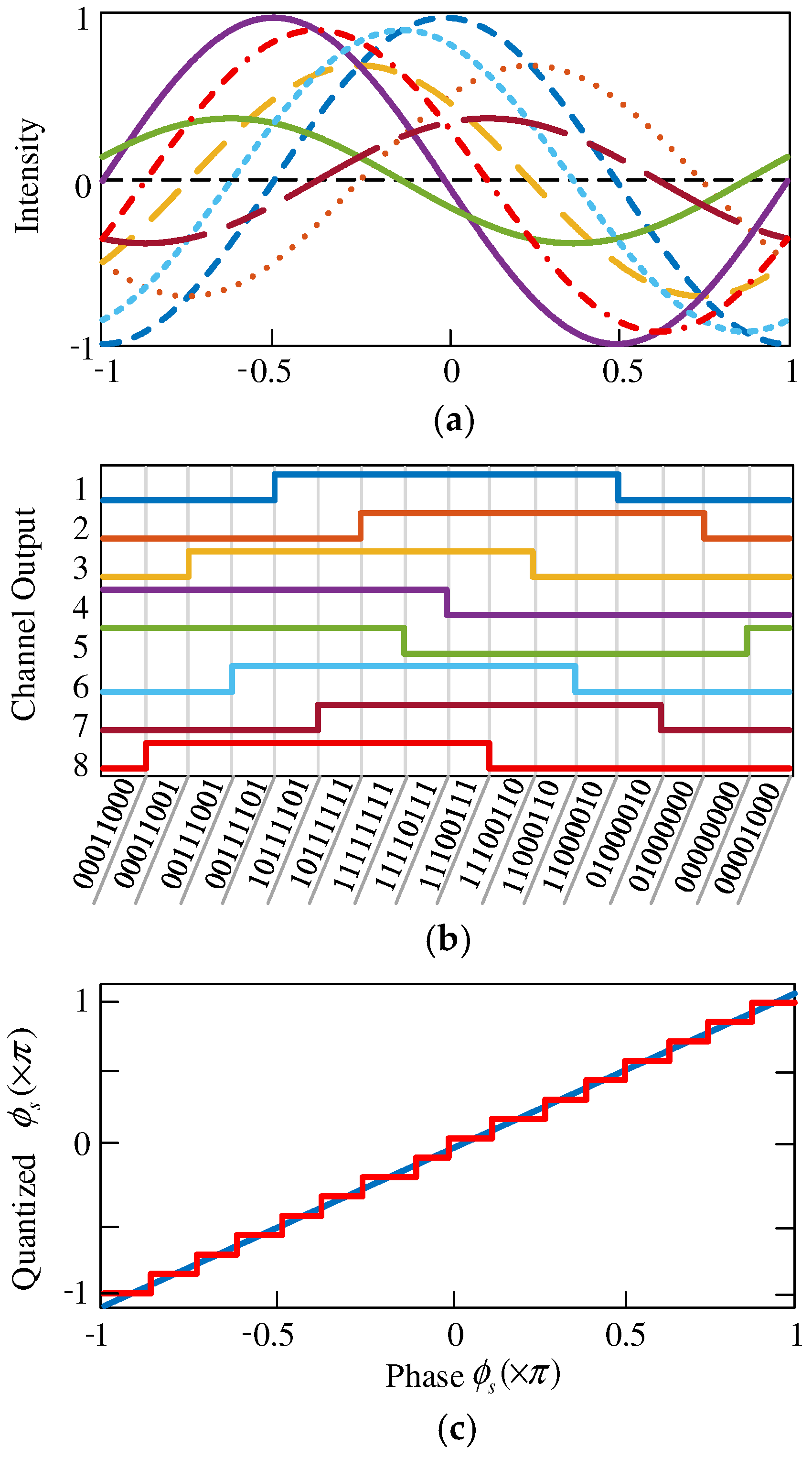
It can be seen from the above equation that the minimum phase-shift interval between the output channels is π / 8 . Since all output channel signals are zero-mean, the comparator thresholds can be fixed at zero. The transfer functions for the eight output ports are illustrated in Figure 2a. In the quantization stage, a comparator array employs a zero-threshold decision rule to convert these analog signals into 8-channel digital outputs: an input signal exceeding the threshold is mapped to ‘1’, while those below are assigned ‘0’. The coding mechanism, depicted in Figure 2b, naturally yields a Gray code output. By ensuring that adjacent codewords differ by only a single bit, this scheme effectively minimizes readout errors at decision boundaries and enhances the robustness of high-speed conversion. The dependence of the quantized value on the phase shift induced by the input signal is shown in Figure 2c, where a linear relationship may be observed.
Generally, to achieve a bit resolution of N ( N 5 ), only 2 N 3 DOMZMs are required. Compared with conventional parallel phase-shifting schemes requiring 2 N 1 modulators [24], this architecture achieves significant hardware simplification. For an N -bit system, the number of required DOMZMs is denoted as M = 2 N 3 . The bias phases applied to each modulator should have uniform spacing, with a phase increment defined as:
Δ ϕ b = π 2 N 3
The bias phase ϕ b k of the k-th DOMZM ( 1 k M ) can be expressed as ϕ b k = ( k 1 ) Δ ϕ b . The photocurrent signals generated by the two complementary output ports of the k-th DOMZM can be represented as follows:
I k , 1 = I 0 [ 1 + cos ( ϕ s + ϕ b k ) ]
I k , 2 = I 0 [ 1 cos ( ϕ s + ϕ b k ) ]
The linear combination module needs to generate 2 N 1 output ports to achieve quantization. To refine the quantization intervals, in addition to directly utilizing the differential outputs of each DOMZM, an intermediate signal S int must be introduced. For instance, in a 5-bit system, the intermediate signal can be generated by combining the positive output signals of the first and second modulators, which is
S int = α ( I 1 , 1 + I 2 , 1 ) + β
where the coefficients α and β are used to normalize the amplitude and align the dc components. By performing cross-differential operations between the intermediate signal S int and the primary signals from each DOMZM, the module eventually generates 2 N 1 parallel signals. Since all differential output signals possess a zero-mean property, the decision thresholds for the subsequent comparator array can be uniformly fixed at zero.

3. Results and Discussion

3.1. Proof-of-Concept Experiment

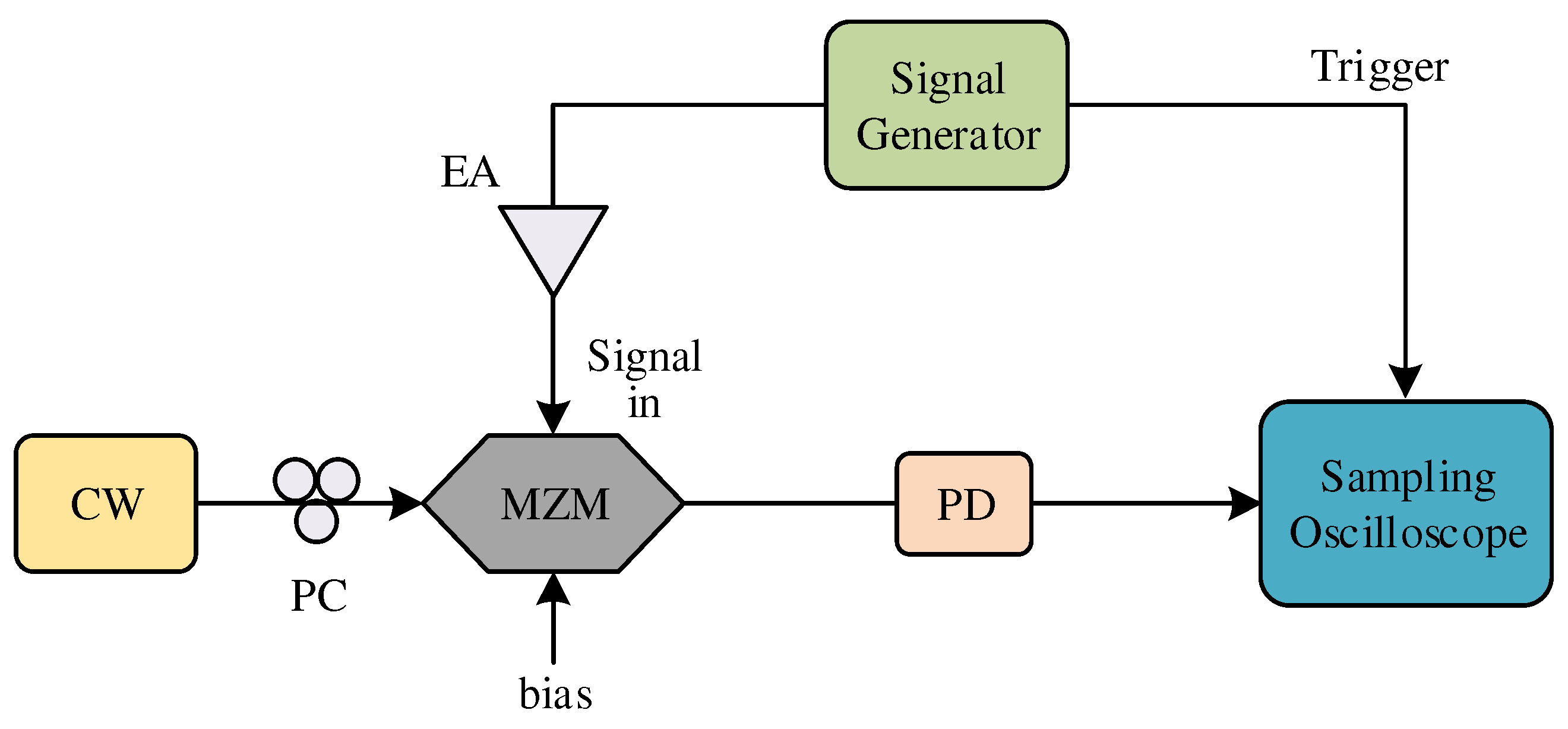
We implemented proof-of-concept experiments to verify the principle of the proposed photonic quantization scheme. The experimental setup is shown in Figure 3. In the experiment, a continuous-wave light generated by a tunable laser source (IDPhotonics) operating at 1550 nm was utilized as the optical carrier. This was modulated by an analog signal via an MZM (Avanex 792000450) with a half-wave voltage of 1.8 V. A polarization controller was employed to minimize the polarization-dependent loss of the modulator. The analog signal to be quantized was generated by a signal generator (R&S SMB100A). The signal from the signal generator was injected into a microwave amplifier (Ceyear 3871FS). After amplification, it was then fed into the MZM. After optical-to-electrical conversion performed by a PD (KG-PD-10G), the output time-domain waveforms were captured by a digital sampling oscilloscope (Keysight 86100D). To emulate the multi-channel parallel sampling architecture, a sequential bias-tuning and offline synthesis approach was adopted. Specifically, the dc bias of the MZM was adjusted to meet the required phase shifts for each channel, with the corresponding waveforms being recorded individually. To ensure temporal alignment across different measurements, the sampling oscilloscope was triggered by a reference signal from the signal generator. The linear combination and encoding processes were carried out through offline data processing in a computer program.
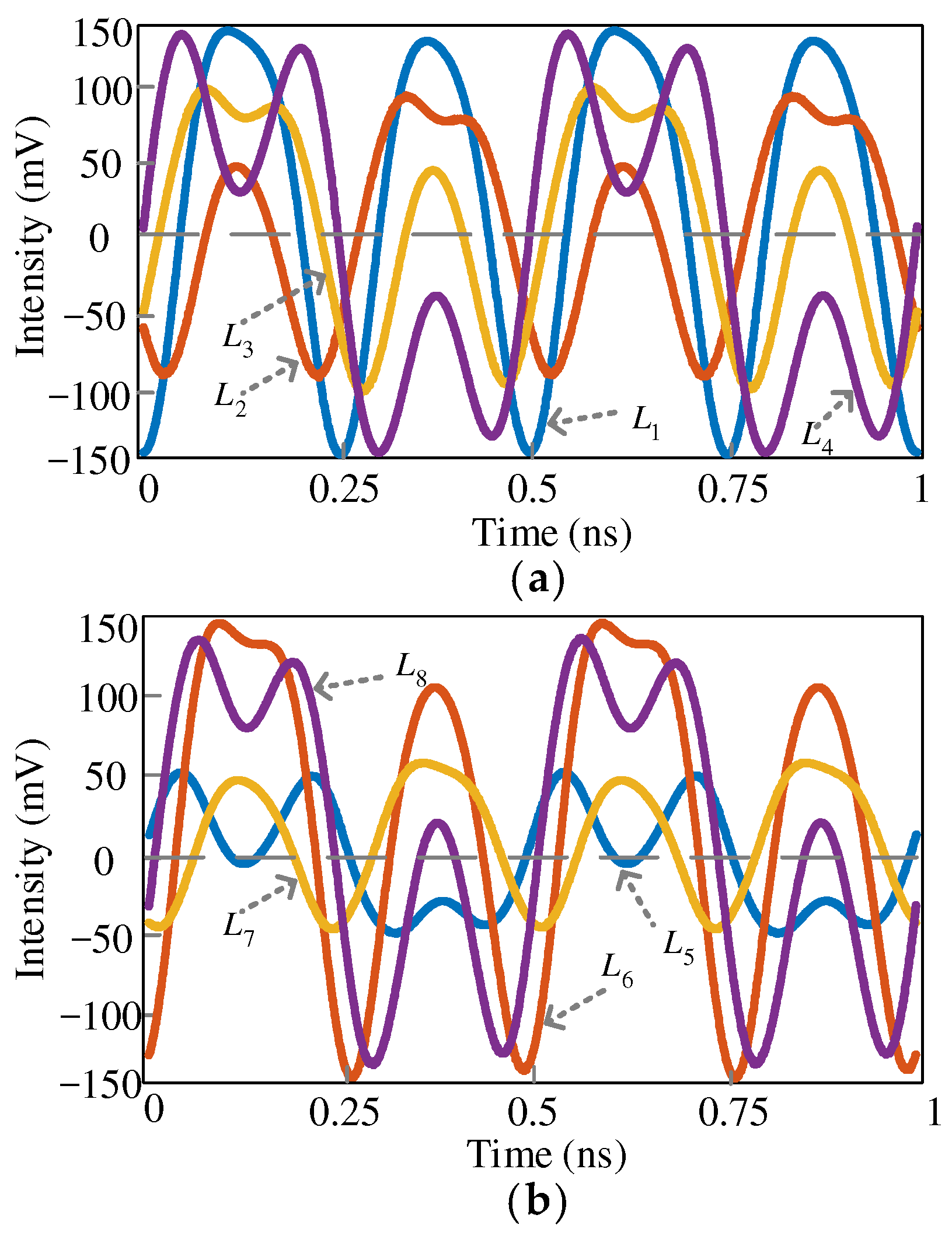
In the experiment, the analog signal to be quantized was a 2 GHz sinusoidal signal. In order to demonstrate a 4-bit photonic quantization, the dc bias of the MZM was sequentially adjusted to four specific points, corresponding to phase shifts of 0, π/2, π, and 3π/2, and the corresponding output waveforms were each recorded. Considering that harmonics may occur under different bias conditions, the 10 GHz bandwidth of the PD still meets the requirements. The experimental results of the proposed 4-bit quantization are given in Figure 4. By performing offline linear combination operations on the captured waveforms, eight parallel channel signals ( L 1 to L 8 ) were successfully generated; these are shown in Figure 4a,b. After the thresholding decision of the comparators, 8-bit Gray code outputs corresponding to their amplitude levels could be obtained.
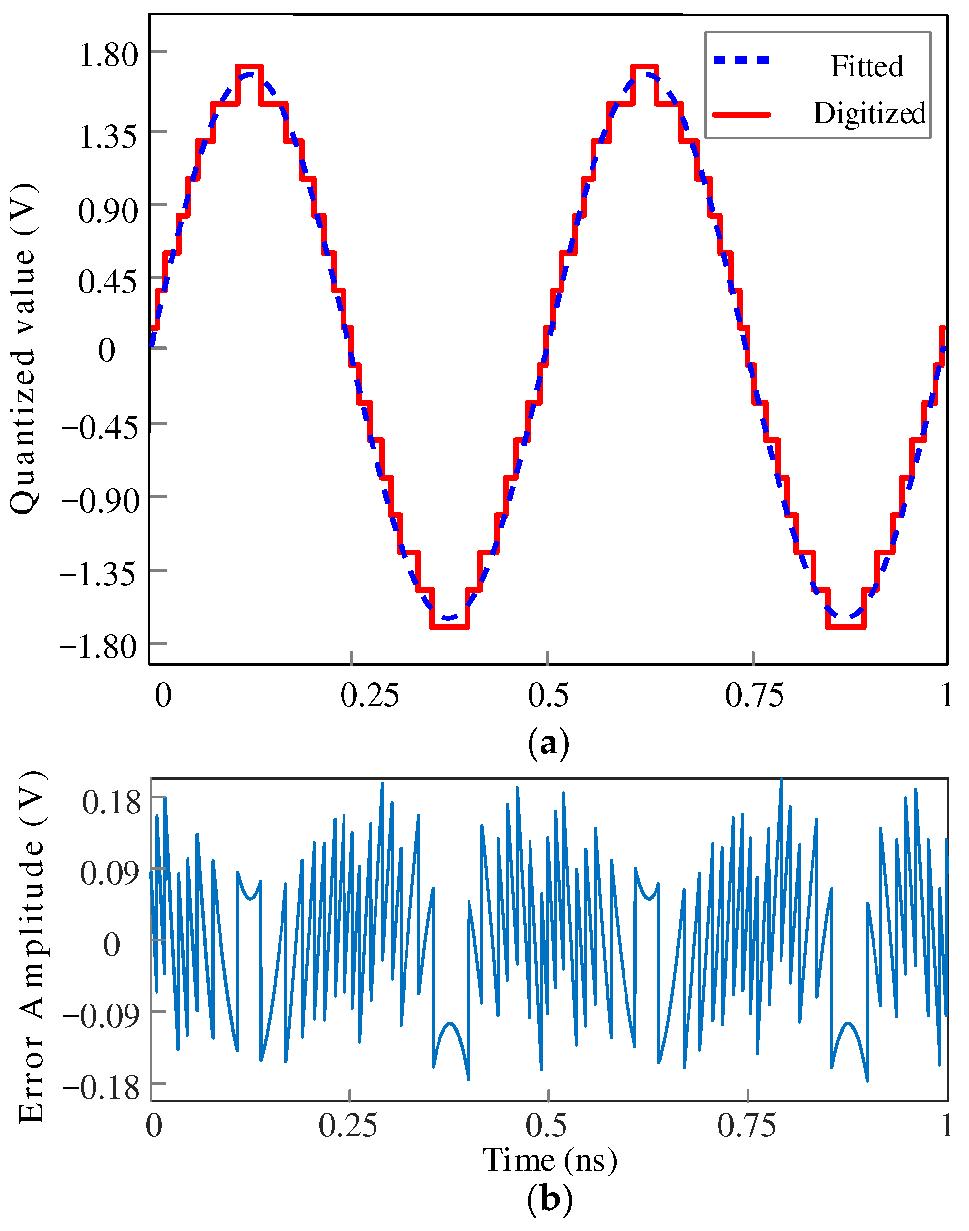
By implementing a look-up table mapping process, a quantized waveform could be obtained. This is shown in Figure 5a, where it may be seen that the quantized waveform shows good agreement with the fitted sinusoidal signal, successfully achieving a quantization level of 16 for the 2 GHz signal input. Figure 5b provides the quantization error along the time axis. The results demonstrate that the majority of error fluctuations are strictly confined within the theoretical limits of ± 0.5 least significant bit (LSB). The minor performance degradation compared to the ideal 4-bit quantization, as well as occasional error spikes, are primarily attributed to bias phase errors in the modulators and noise in the detection process. The signal-to-noise ratio (SNR) of the quantized waveform was estimated to be approximately 22.97 dB, which corresponds to an effective number of bits (ENOB) of 3.52. The experimental results demonstrate the correctness and feasibility of the proposed photonic quantization principle.

3.2. Error Tolerance Analysis and Impact of Receiver Bandwidth

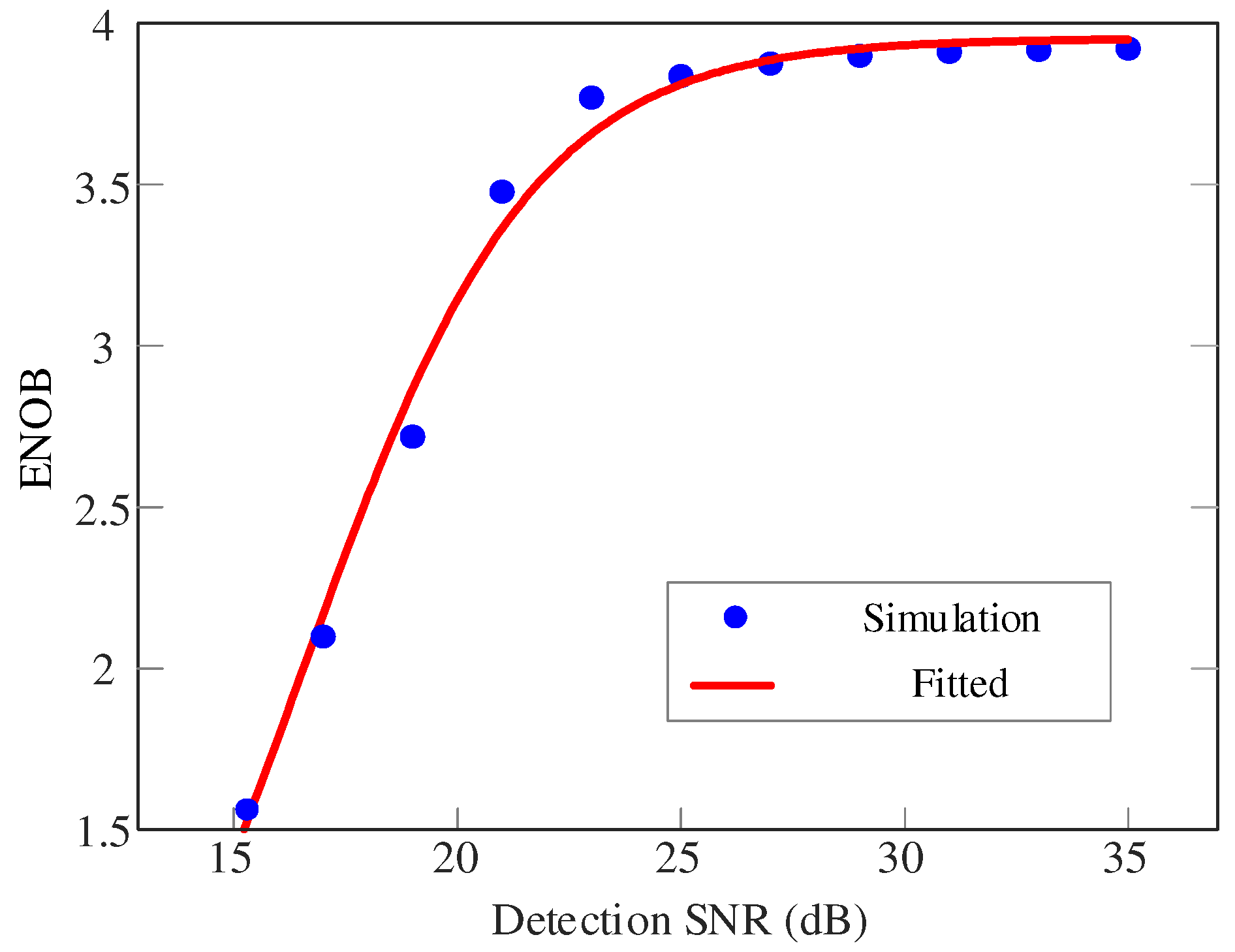
The experimental results indicate that both bias phase error and system noise affect quantization performance. Accordingly, we conducted a systematic simulation to study the influence of these two factors. First, we investigated the impact of system noise. In the simulation, a 2 GHz signal was employed as the analog signal to quantized, 4-bit quantization was considered, and the bandwidth of the receiver was set to 10 GHz, all of which were similar to the experimental conditions. We added additive white Gaussian noise to electrical signals after the PDs and obtained ENOB values under different SNR conditions. The result of ENOB vs. SNR is shown in Figure 6. It may be seen that in the low-SNR region (e.g., SNR < 15 dB), system performance is severely limited, with the ENOB far below the ideal bit resolution. As the SNR increases, the simulated ENOB grows monotonically and gradually approaches the ideal limit of 4 bits. When the SNR is 20 dB, the ENOB decreases by approximately 0.7 bits compared to the ideal bit resolution.
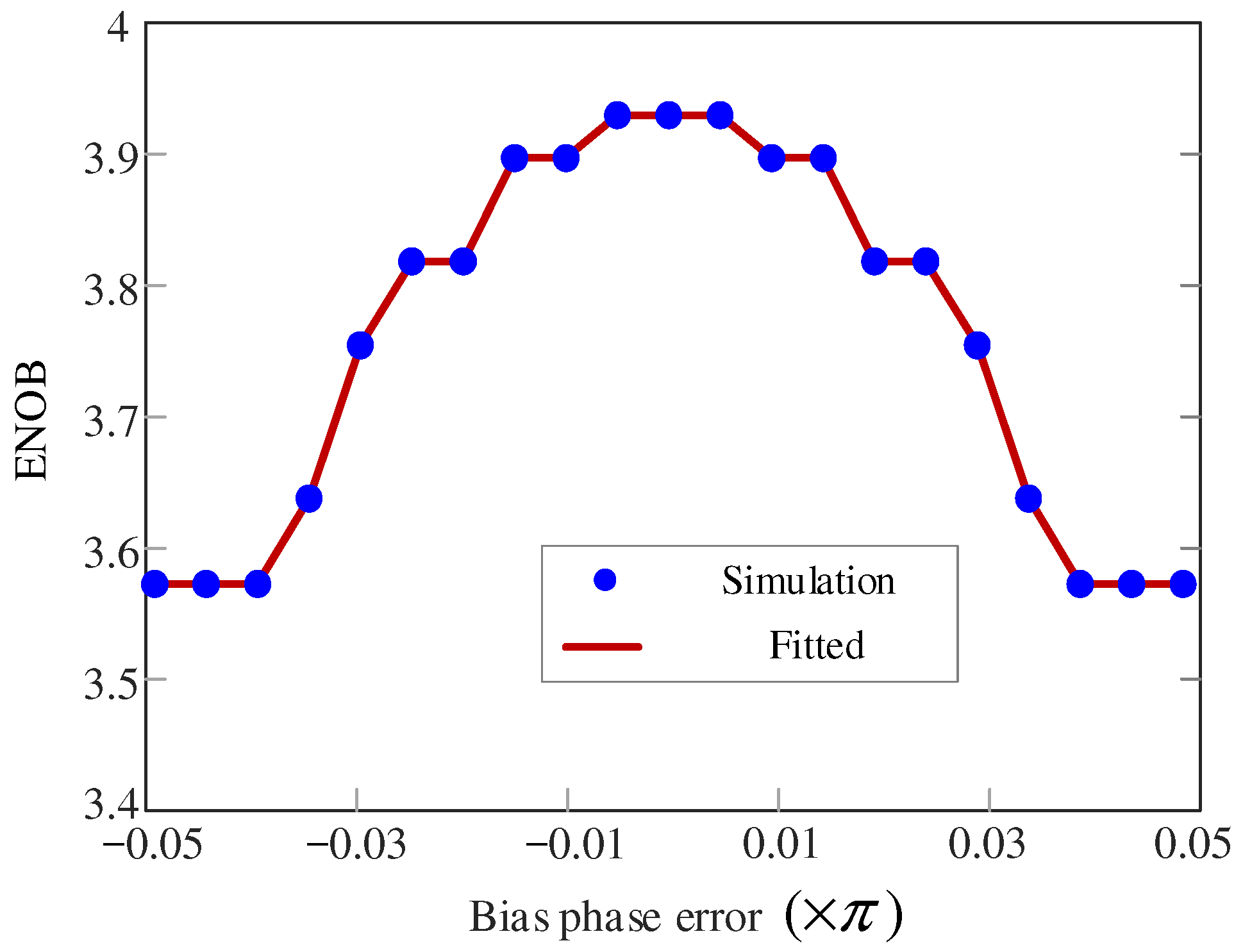
Next, we investigated the bias phase error induced by the MZM bias voltage error on quantization performance. The simulation conditions were set to be the same as those in the previous simulation. In the simulation, the bias phase of one DOMZM is set to deviate from the ideal value, whereas the other DOMZM is maintained with no deviation. The bias phase error is defined as δ ϕ = π × δ V / V π , where δ V is the bias voltage error (the value deviated from the ideal voltage). The result of ENOB vs. bias phase error is shown in Figure 7. It may be seen that a phase deviation of 0.05 π in a single MZM causes the ENOB to drop to around 3.57 bits. These findings underscore the necessity of precisely locking the bias voltage of each MZM to an optimal operating point, to mitigate the detrimental impact of phase errors on system performance.
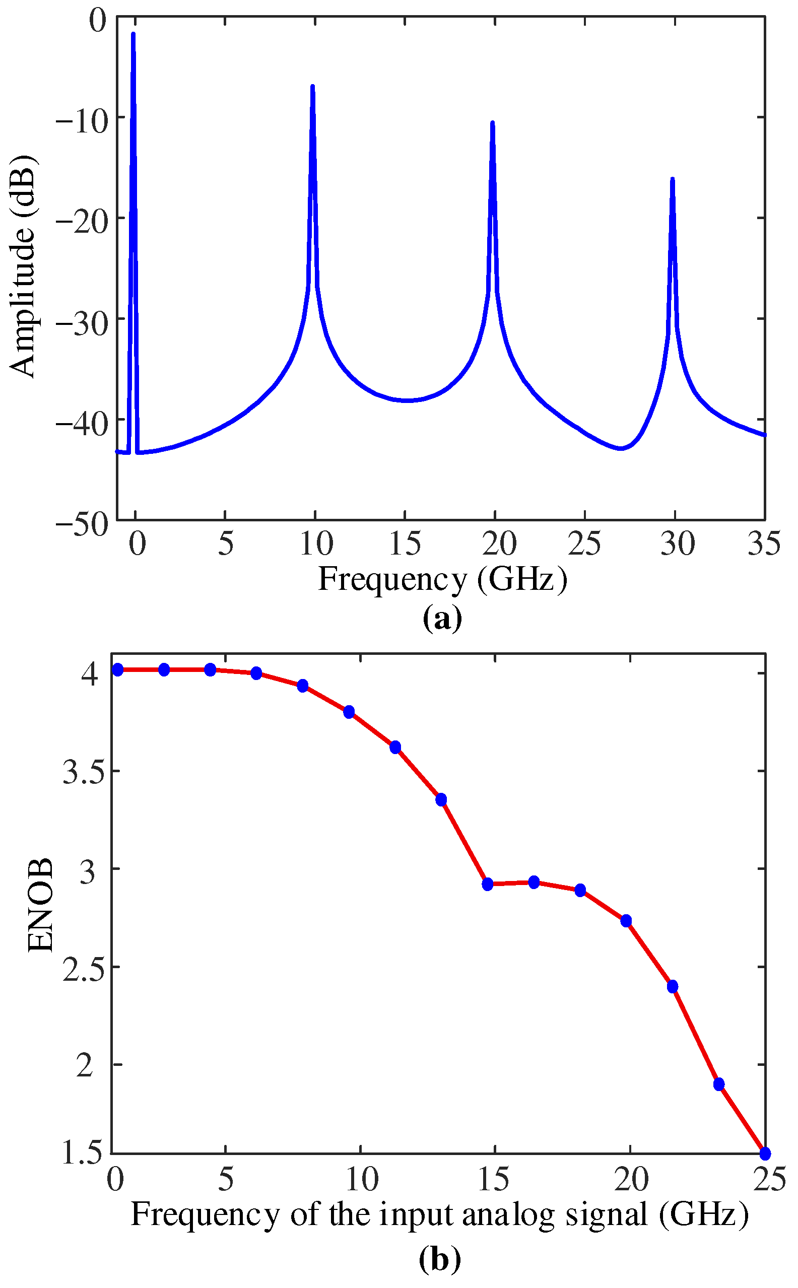
In the MZM-based quantization, after the signal is modulated via the MZM, multiple orders of harmonics are generated, imposing high bandwidth requirements on the receiver (including the PD and processing circuits). Figure 8a shows the generation of harmonics when the input signal is a 10 GHz sinusoidal signal and the MZM is biased at π / 4 . To investigate the impact of the receiver bandwidth on the quantization performance, we conducted further simulations. In the simulation, the receiver bandwidth is set to 40 GHz, while the input analog signals to be quantized ranged from 1 GHz to 25 GHz. Noise was excluded in the simulation. As illustrated in Figure 8b, the ENOB undergoes a sharp decline for input signals exceeding 10 GHz. The underlying cause is the generation of high-order harmonics stemming from the MZM’s inherent nonlinearity, which significantly increases the requirement on the receiver bandwidth. This issue is also a common challenge for phase-shifting photonic quantization based on MZMs.

3.3. Performance Comparison

We compare the scheme proposed in this paper with typical phase-shifting photonic quantization and its improved solutions, as shown in Table 1. To facilitate comparison, we first define an optical system complexity index N, which is the sum of the electro-optic modulators and PDs used in the scheme. The typical schemes compared include a phase-shifting quantization approach with spatial optical interference scheme [23], an approach using identical half-wave voltages [24], an improved scheme using additional MZM [28] and an improved scheme with post processing [29]. It can be seen from the table that the optical complexity index of the proposed scheme is roughly comparable to that of the two improved schemes, but much smaller than that of the conventional phase-shifting photonic quantization schemes [23,24]. It should be pointed out that the scheme in [28] includes an optical phase-shifting module, which is relatively complex and is not reflected in the aforementioned optical complexity index N. In addition, the threshold of the comparators in the scheme of [29] is related to the input optical power. Compared to schemes that do not require an optical phase shifting module, our proposed architecture utilizes fewer modulators. For example, the scheme using MZM array require 2 n 1 modulators to achieve n-bit quantization [24], while the improved scheme with post processing requires 2 n 3 + 1 modulators [29]. In contrast, our scheme only needs 2 n 3 modulators. Moreover, with fewer modulators employed, our scheme utilizes differential encoding to effectively counteract optical power fluctuations. Therefore, considering both system performance and complexity, the proposed scheme in this work is competitive.

3.4. Challenges to Practical Deployment

The key to the linear combination module lies in achieving precise mathematical operations. In practical circuits, this typically necessitates an analog signal processing chain composed of broadband amplifiers, analog adders, and programmable gain amplifiers used to implement operations such as addition, subtraction and coefficient scaling. The entire circuit must exhibit high linearity and low noise characteristics to ensure quantization precision. In addition, ensuring a sufficient and flat bandwidth across the entire signal chain from the PDs to the combination circuit is critical; otherwise, signal distortion and quantization performance degradation will result.
Regarding the practical transition toward a photonic integrated circuit platform, most discrete components in this architecture, including the DOMZMs, PDs, linear combination module, and comparator arrays, are highly compatible with silicon photonic integration technology. However, achieving a fully integrated system remains challenging, primarily due to the pulsed laser source which is currently difficult to implement on-chip with high performance. Despite the hurdle of integrating the pulse generation system, the feasibility of migrating the core processing components to a silicon photonic chip underscores the potential of this architecture for future scalable and compact implementations.

4. Conclusions

In summary, we propose here a compact and hardware-efficient photonic quantization scheme utilizing DOMZMs and a linear combination module. By leveraging the complementary nature of DOMZM output ports and implementing a novel cross-channel differential linear combination operation, the presented approach can improve the number of bits while using the same number of modulators. At the same time, the scheme also avoids complex optical phase-shifting components and enables adaptive decision threshold setting, meaning that the threshold level is independent of the input optical power. Proof-of-concept experiments with 4-bit quantization were successfully demonstrated. The experimental results fully confirmed the correctness of the principle and the feasibility of the scheme. Further performance evaluation, including the impact on performance of noise, bias point drift of a single DOMZM, and receiver bandwidth in terms of ENOB, was carried out through simulations. We also discussed the challenges to practical deployment of the proposed approach. We believe that the proposed scheme provides a competitive solution for photonic quantization.

Author Contributions

Conceptualization, D.W.; methodology, H.Z.; software, D.W.; formal analysis, D.W.; resources, H.C.; writing—original draft preparation, D.W.; writing—review and editing, D.W.; visualization, H.Z.; supervision, H.C.; funding acquisition, H.C. All authors have read and agreed to the published version of the manuscript.

Funding

This research was funded by Applied Basic Research Program “Xinmiao” Project of Zhejiang province, China, National Natural Science Foundation of China (62375071, 62475064), Natural Science Foundation of Zhejiang Province (LZ25F010005, LMS26F010013).

Institutional Review Board Statement

Not applicable.

Data Availability Statement

Data underlying the results presented in this paper are not publicly available at this time but may be obtained from the authors upon reasonable request.

Conflicts of Interest

The authors declare no conflicts of interest.

References

  1. Walden, R. Analog-to-digital converter survey and analysis. IEEE J. Sel. Areas Commun. 1999, 17, 539–550. [Google Scholar] [CrossRef]
  2. Yang, G.; Zou, W.; Yu, L.; Qian, N.; Chen, J. Investigation of electronic aperture jitter effect in channel-interleaved photonic analog-to-digital converter. Opt. Express 2019, 27, 9205–9214. [Google Scholar] [CrossRef]
  3. Valley, G.C. Photonic analog-to-digital converters. Opt. Express 2007, 15, 1955–1982. [Google Scholar] [CrossRef] [PubMed]
  4. Chan, E.H.; Minasian, R.A. Microwave photonic downconverter with high conversion efficiency. J. Light. Technol. 2012, 30, 3580–3585. [Google Scholar] [CrossRef]
  5. Ghelfi, P.; Laghezza, F.; Scotti, F.; Serafino, G.; Capria, A.; Pinna, S.; Onori, D.; Porzi, C.; Scaffardi, M.; Malacarne, A. A fully photonics-based coherent radar system. Nature 2014, 507, 341–345. [Google Scholar] [CrossRef] [PubMed]
  6. Zou, X.; Lu, B.; Pan, W.; Yan, L.; Stöhr, A.; Yao, J. Photonics for microwave measurements. Laser Photonics Rev. 2016, 10, 711–734. [Google Scholar] [CrossRef]
  7. Pan, S.; Zhang, Y. Microwave photonic radars. J. Light. Technol. 2020, 38, 5450–5484. [Google Scholar] [CrossRef]
  8. Li, M.; Hao, T.; Li, G.; Wang, A.; Dai, Y.; Li, W.; Capmany, J.; Yao, J.; Zhu, N.; Li, M. Time-variant parity-time symmetry in frequency-scanning systems. Laser Photonics Rev. 2024, 15, 8710. [Google Scholar] [CrossRef]
  9. Chen, S.; Lan, X.; Xu, H.; Yang, Z.; Wang, X.; Yin, F.; Xu, K.; Li, M.; Dai, Y. Broadband phased array receiver based on microwave photonics channelization. Photonics Res. 2026, 14, 626–634. [Google Scholar] [CrossRef]
  10. Luo, H.; Yu, J.; Wang, J.; Ma, C.; Han, X.; Su, X. High-precision micro-displacement sensing based on an optical filter and optoelectronic oscillators. Opt. Express 2023, 31, 19278–19292. [Google Scholar] [CrossRef]
  11. Yang, G.; Zou, W.; Yu, L.; Chen, J. Influence of the sampling clock pulse shape mismatch on channel-interleaved photonic analog-to-digital conversion. Opt. Lett. 2018, 43, 3530–3533. [Google Scholar] [CrossRef] [PubMed]
  12. Citrin, D.S. Photonic Sampling analog-to-digital conversion with read-in timing jitter. IEEE Trans. Commun. 2021, 70, 445–454. [Google Scholar] [CrossRef]
  13. Li, Z.; Wang, X.; Zhang, Y.; Shang, C.; Lyu, W.; Lyu, Y.; Zeng, C.; Zhang, Z.; Zhang, S.; Li, H. Photonic sampling analog-to-digital conversion based on time and wavelength interleaved ultra-short optical pulse train generated by using monolithic integrated LNOI intensity and phase modulator. Opt. Express 2022, 30, 29611–29620. [Google Scholar] [CrossRef]
  14. Tu, D.; Huang, X.; Yu, H.; Yin, Y.; Yu, Z.; Wei, Z.; Li, Z. Photonic sampled and quantized analog-to-digital converters on thin-film lithium niobate platform. Opt. Express 2023, 31, 1931–1942. [Google Scholar] [CrossRef]
  15. Han, Y.; Jalali, B. Photonic time-stretched analog-to-digital converter: Fundamental concepts and practical considerations. J. Light. Technol. 2003, 21, 3085. [Google Scholar] [CrossRef]
  16. Peng, D.; Zhang, Z.; Ma, Y.; Zhang, Y.; Zhang, S.; Liu, Y. Broadband linearization in photonic time-stretch analog-to-digital converters employing an asymmetrical dual-parallel Mach-Zehnder modulator and a balanced detector. Opt. Express 2016, 24, 11546–11557. [Google Scholar] [CrossRef] [PubMed]
  17. Jiang, T.; Wang, L.; Li, J. High-resolution timing jitter measurement based on the photonics time stretch technique. Opt. Express 2023, 31, 6722–6729. [Google Scholar] [CrossRef]
  18. Zhou, Y.; Chan, J.C.; Jalali, B. A unified framework for photonic time-stretch systems. Laser Photonics Rev. 2022, 16, 2100524. [Google Scholar] [CrossRef]
  19. Taylor, H. An optical analog-to-digital converter-design and analysis. IEEE J. Quant. Electron. 1979, 15, 210–216. [Google Scholar] [CrossRef]
  20. Gong, S.; Wang, X.; Wang, H.; Chen, G.; Zhong, K.; Guo, C.; Zhang, G.; Liu, L. All-optical analog-to-digital converters based on a thin-film lithium niobate modulator and a star coupler. Photon. Res. 2025, 13, 3444–3452. [Google Scholar] [CrossRef]
  21. Jalali, B.; Xie, Y. Optical folding-flash analog-to-digital converter with analog encoding. Opt. Lett. 1995, 20, 1901–1903. [Google Scholar] [CrossRef]
  22. Golani, O.; Mauri, L.; Pasinato, F.; Cattaneo, C.; Consonnni, G.; Balsamo, S.; Marom, D.M. A photonic analog-to-digital converter using phase modulation and self-coherent detection with spatial oversampling. Opt. Express 2014, 22, 12273–12282. [Google Scholar] [CrossRef] [PubMed]
  23. Stigwall, J.; Galt, S. Demonstration and analysis of a 40-gigasample/s interferometric analog-to-digital converter. J. Light. Technol. 2006, 24, 1247. [Google Scholar] [CrossRef]
  24. Chi, H.; Yao, J. A photonic analog-to-digital conversion scheme using Mach-Zehnder modulators with identical half-wave voltages. Opt. Express 2008, 16, 567–572. [Google Scholar] [CrossRef] [PubMed]
  25. Wu, Q.; Zhang, H.; Yao, M.; Zhou, W. All-optical analog-to-digital conversion using inherent multiwavelength phase shift in LiNbO phase modulator. IEEE Photon. Technol. Lett. 2008, 20, 1036–1038. [Google Scholar] [CrossRef]
  26. Wu, Q.; Zhang, H.; Peng, Y.; Fu, X.; Yao, M. 40GS/s Optical analog-to-digital conversion system and its improvement. Opt. Express 2009, 17, 9252–9257. [Google Scholar] [CrossRef] [PubMed]
  27. Yang, S.; Wang, C.; Chi, H.; Zhang, X.; Zheng, S.; Jin, X.; Yao, J. Photonic analog-to-digital converter using Mach–Zehnder modulators having identical half-wave voltages with improved bit resolution. Appl. Opt. 2009, 48, 4458–4467. [Google Scholar] [CrossRef]
  28. Wang, Y.; Zhang, H.; Wu, Q.; Yao, M. Improvement of photonic ADC based on phase-shifted optical quantization by using additional modulators. IEEE Photon. Technol. Lett. 2012, 24, 566–568. [Google Scholar] [CrossRef]
  29. He, H.; Chi, H.; Yu, X.; Jin, T.; Zheng, S.; Jin, X.; Zhang, X. An improved photonic analog-to-digital conversion scheme using Mach–Zehnder modulators with identical half-wave voltages. Opt. Commun. 2018, 425, 157–160. [Google Scholar] [CrossRef]
  30. Sarantos, C.H.; Dagli, N. A photonic analog-to-digital converter based on an unbalanced Mach-Zehnder quantizer. Opt. Express 2010, 18, 14598–14603. [Google Scholar] [CrossRef]
  31. Chi, H.; Li, Z.; Zhang, X.-M.; Zheng, S.; Jin, X.; Yao, J. Proposal for photonic quantization with differential encoding using a phase modulator and delay-line interferometers. Opt. Lett. 2011, 36, 1629–1631. [Google Scholar] [CrossRef] [PubMed]
  32. Peng, Y.; Zhang, H.; Wu, Q.; Fu, X.; Yao, M. Adaptive thresholding scheme in photonic analog-to-digital conversion. Opt. Lett. 2009, 34, 2201–2203. [Google Scholar] [CrossRef] [PubMed]
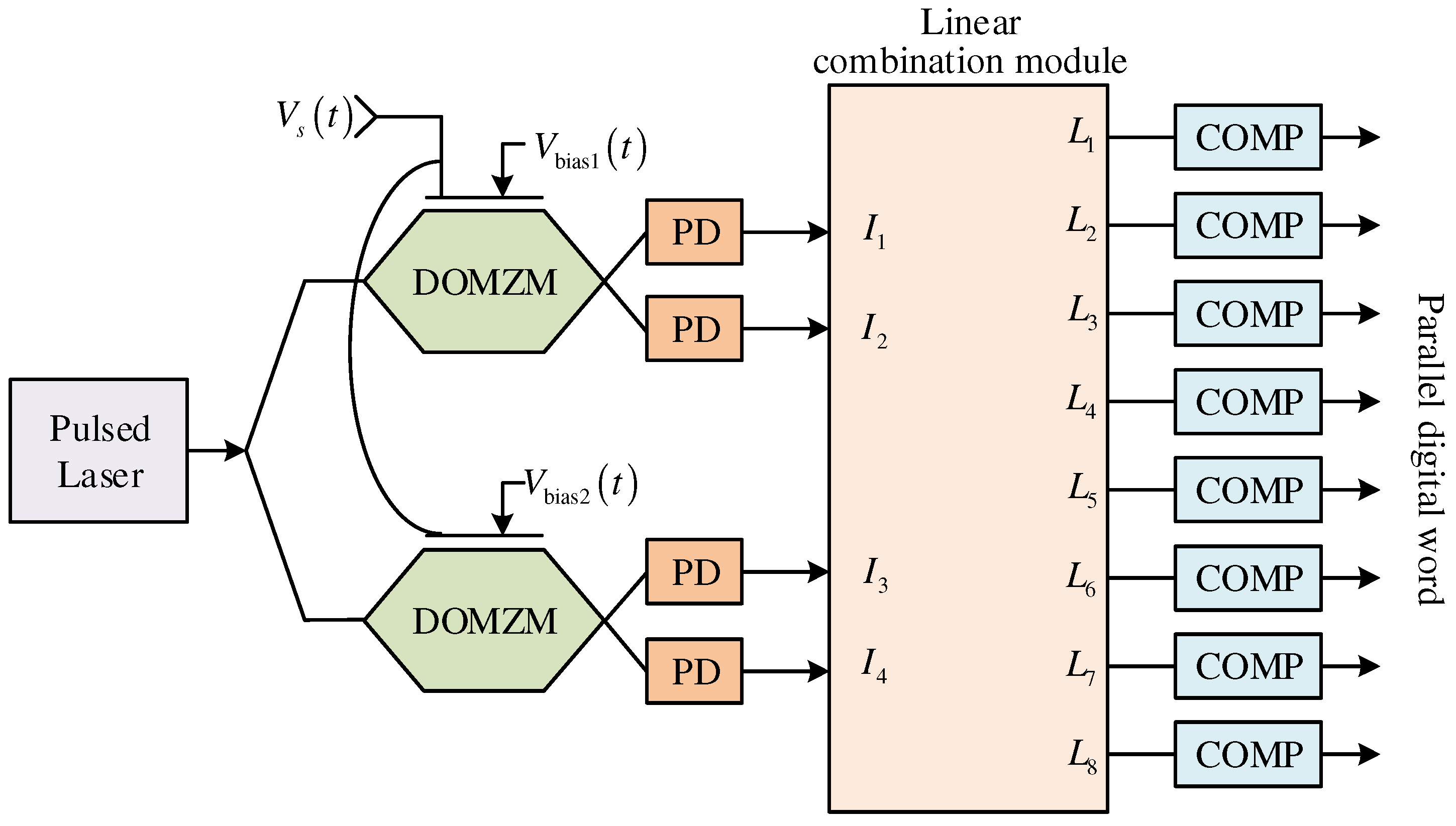
Figure 1. Schematic diagram of the proposed 4-bit photonic quantization scheme. PD—photodetector; DOMZM—dual-output Mach–Zehnder modulator; COMP—comparator.
Photonics 13 00461 g001
Figure 2. Coding and quantization principle of the proposed photonic quantization with a 4-bit resolution. (a) The transfer curves of eight output ports from L 1 to L 8 ; (b) Binary outputs from the comparator array; (c) The phase shift ϕ s induced by the input voltage signal vs. the quantized value.
Photonics 13 00461 g002
Figure 3. Experimental setup for proof-of-concept photonic quantization using sequential bias-tuning. CW—continuous-wave laser; PC—polarization controller; EA—electrical amplifier; PD—photodetector.
Photonics 13 00461 g003
Figure 4. (a) The time-domain waveforms of channels 1 to 4; (b) The time-domain waveforms of channels 5 to 8.
Photonics 13 00461 g004
Figure 5. (a) The quantized signal compared with the fitted sinusoidal signal. (b) The quantization error along the time axis.
Photonics 13 00461 g005
Figure 6. Impact of noise on quantization performance (ENOB vs. SNR of the signals after PD).
Photonics 13 00461 g006
Figure 7. Impact of the bias phase error on quantization performance (ENOB vs. bias phase error of a single MZM).
Photonics 13 00461 g007
Figure 8. (a) Generation of harmonics with a 10 GHz input signal when the MZM is biased at π / 4 . (b) ENOB vs. signal frequency for a given receiver bandwidth of 40 GHz.
Photonics 13 00461 g008
Table 1. Comparison of the complexity index N among five typical photonic quantization schemes based on phase-shifting quantization.
Bit456n
N
Scheme
Scheme using spatial interference scheme [23]91733 2 n 1 + 1
Scheme using MZM
array [24]
163264 2 n
Improved scheme using additional MZM [28]71119 2 n 2 + 3
Improved scheme with post processing [29]61018 2 n 2 + 2
This work61224 2 n 2 + 2 n 3
Disclaimer/Publisher’s Note: The statements, opinions and data contained in all publications are solely those of the individual author(s) and contributor(s) and not of MDPI and/or the editor(s). MDPI and/or the editor(s) disclaim responsibility for any injury to people or property resulting from any ideas, methods, instructions or products referred to in the content.