
Article

High-Extinction-Ratio Electro-Optic Modulator on Thin-Film Lithium Niobate Operating at 1064 nm


State Key Laboratory of Precision Measuring Technology and Instruments, Key Laboratory of Opto-electronic Information Technology of Ministry of Education, Tianjin Key Laboratory of Integrated Opto-electronics Technologies and Devices, School of Precision Instruments and Opto-electronics Engineering, Tianjin University, Tianjin 300072, China
*
Author to whom correspondence should be addressed.
Photonics 2026, 13(5), 505; https://doi.org/10.3390/photonics13050505
Submission received: 25 April 2026 / Revised: 17 May 2026 / Accepted: 19 May 2026 / Published: 21 May 2026
(This article belongs to the Special Issue Microwave Photonics: Advances and Applications)

Abstract

Laser sources emitting light at 1064 nm enable key applications in lidar, quantum photonics, and remote sensing, where high-extinction-ratio intensity modulation is desired to suppress the leakage light at the “off” states during modulation. Here we demonstrate a 1064 nm thin-film lithium niobate (TFLN) Mach–Zehnder electro-optic modulator featuring a half-wave voltage–length product of 2.1 V·cm and a measured electro-optic 3 dB bandwidth exceeding 10 GHz. By optimizing the waveguide and MMI-based interferometer design to improve device balance, we achieve an extinction ratio exceeding 30 dB without thermal tuning. This high extinction ratio enables high-contrast optical modulation at 1064 nm, which is essential for optical switching and other photonic applications requiring high on–off contrast.

1. Introduction

Lasers operating at 1064 nm, supported by mature Nd/YAG and Yb-doped fiber technologies, are widely used in Light Detection and Ranging (lidar) and fiber-optic sensing systems [1,2,3]. High-performance electro-optic modulators (EOMs) are essential for these applications to achieve precise optical modulation. In particular, high extinction ratio is required to improve modulation contrast and suppress the leakage light at the “off” states, ensuring high signal fidelity. Compared with the well-established C-band platform for optical fiber communications, the 1064 nm wavelength offers advantages in free-space optical transmission. For a given aperture, the shorter wavelength enables smaller diffraction-limited beam divergence, which is beneficial for long-distance free-space optical links and beam delivery [4,5]. In addition, modulators operating at 1064 nm feature smaller size and lower driving voltage compared with those operating at C-band because of the shorter wavelength.
Conventional silicon photonics is challenged at 1064 nm due to increased absorption near its band edge, which limits silicon-based optical modulators at this wavelength. The reduced design margin near the band edge also makes it difficult to directly transfer mature telecom-band silicon modulator designs to the 1064 nm regime [6]. Lithium niobate (LiNbO3) offers a large Pockels coefficient and a broad transparency window, making it attractive for broadband and low-power-consumption EOMs. Enabled by ion slicing and wafer bonding technologies, thin-film lithium niobate (TFLN) supports tightly confined optical modes and small waveguide dimensions [7,8], which enables electrodes to be placed closer to the waveguides to enhance optical–electrical field overlap and improve modulation efficiency. Over the last decade, TFLN EOMs in the C-band developed rapidly. High-performance EOMs with low driving voltage, high bandwidth, and low optical loss have been reported [7,8,9,10,11,12,13,14,15,16,17]. Despite this progress, demonstrations of TFLN EOMs around 1064 nm remain comparatively scarce [5,18,19,20,21]. EOMs with high extinction ratio at this wavelength are highly desired for leakage-sensitive functions such as high-performance optical switching [22,23], high-frequency chirp generation [24], and BOTDR-based sensing systems [25,26].
In this work, we propose and experimentally demonstrate a 1064 nm TFLN Mach–Zehnder electro-optic modulator. The device exhibits a VπL of 2.1 V·cm and a measured 3 dB bandwidth exceeding 10 GHz. Most notably, by elaborately optimizing the waveguide and MMI-based interferometer, we achieve an extinction ratio exceeding 30 dB without thermal tuning, enabling high-contrast intensity modulation for 1064 nm photonic systems and potential microwave photonic applications at this wavelength.

2. Design and Simulation

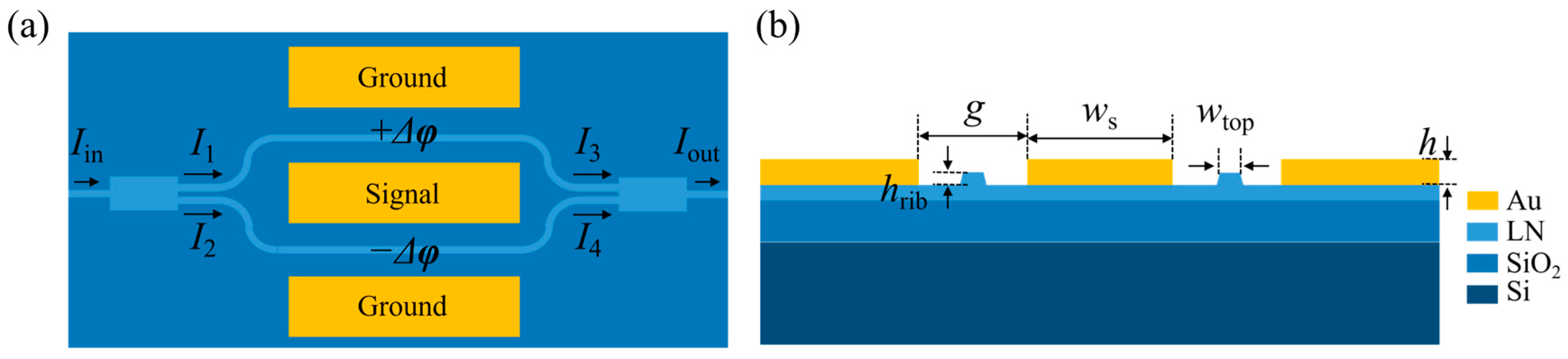
We design a MZI with high extinction ratio based on a TFLN wafer with 300 nm-thick x-cut lithium niobate sitting on top of a 4.7-μm-thick SiO2 buffer layer on a Si substrate. The device is designed in a push–pull configuration as shown in Figure 1a. The voltage applied to the electrodes induces a positive phase change +Δφ in one arm and a negative phase change −Δφ in the other via the electro-optic effect of LN. The cross-sectional structure of the TFLN waveguide and the coplanar waveguide (CPW) electrodes is shown in Figure 1b, including the material stack and key geometric parameters.
When the two light beams from the two arms recombine and interfere at the output, the output intensity Iout can be described by Equation (1):
I ou t   =   I 3   +   I 4   +   2 I 3 I 4   cos ( 2 Δ φ )
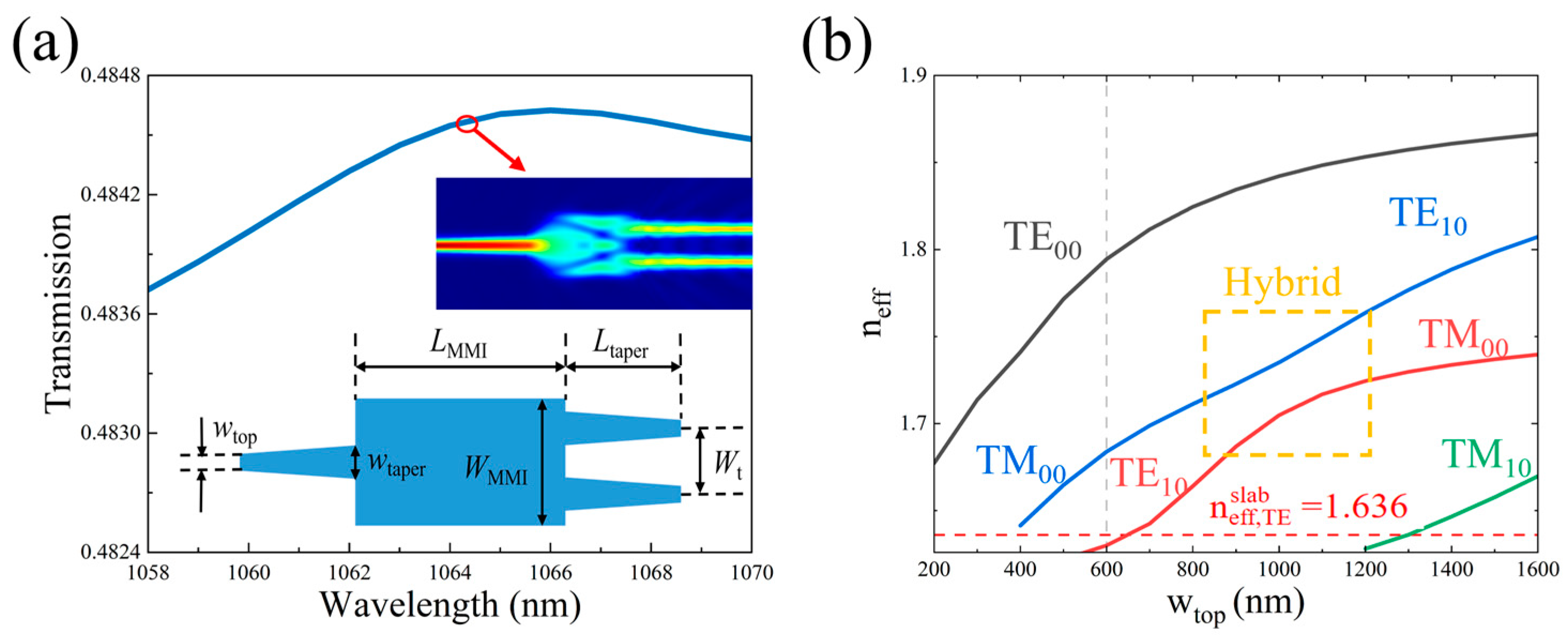
As ER is defined as 10log10(Imax/Imin), it is usually limited by the lowest intensity Imin, which could arise from the unequal light intensities in the two arms. Therefore, we adopt two approaches to achieve high ER: 1. Splitter should have an accurate splitting ratio of 50:50 (I1 = I2); 2. Higher-order waveguide modes should be suppressed to avoid inducing any imbalances between the arms. For approach 1, multimode interference (MMI) used as a splitter is elaborately designed in this work for its higher tolerances to fabrication errors compared with Y branch [27]. The transmission performance and insertion loss of the MMI coupler are analyzed using the finite-difference time-domain (FDTD) method. Perfectly Matched Layer (PML) boundary conditions are applied to suppress spurious reflections. The simulation employs the early shutoff feature with a minimum field threshold of 1 × 10⁻⁵ to improve computational efficiency. These settings ensure accurate modeling of the optical field propagation and interference within the coupling region while maintaining numerical efficiency. The optimized MMI for TE00 mode with a splitting ratio of 50:50 has a length, LMMI, of 18.3 μm, a top width, WMMI, of 4.3 μm, a gap between waveguides, Wt, of 2.2 μm, an etching depth, hrib, of 150 nm, the length of input/output taper, Ltaper, of 15.8 μm and a width, wtaper, of 1.2 μm. The total insertion loss of MMI at 1064 nm is less than 0.15 dB, indicating that MMI can effectively and equally divide the incident light with high transmittance.
Since the MMI coupler is designed and optimized for TE00 mode, excitation of any higher-order modes would result in different light intensities in the two arms and thus reduce ER. For approach 2, we calculate the effective refractive indices of TE00, TE10, TM00, and TM10 modes as a function of the top width (wtop) of the waveguide in Figure 2b. Near the avoided mode crossing region, coupling between TE and TM modes gives rise to hybrid modes with mixed polarization characteristics. The simulation results show that, when wtop < 700 nm, TE10 mode is not supported. Considering that propagation loss is typically high for small wtop, we ultimately set wtop = 600 nm to ensure single-mode condition for TE polarized light and not inducing high propagation loss.
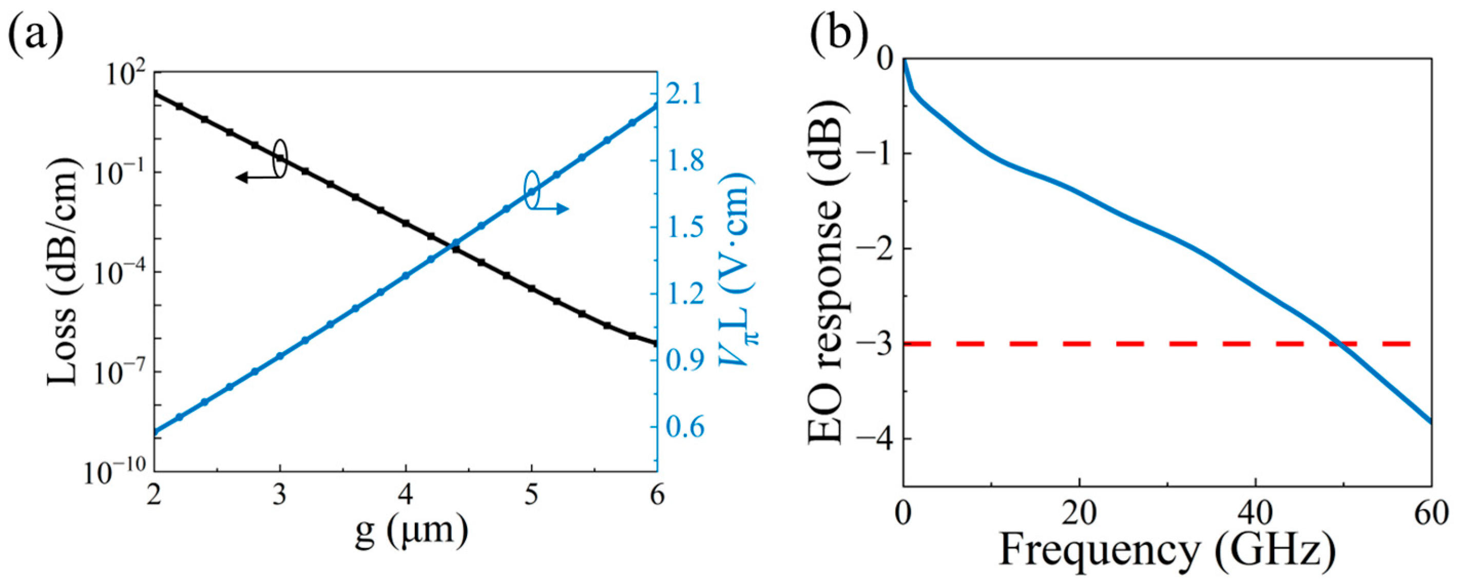
The finite element method (FEM) is employed to simulate optical modes, electrostatic field distribution, and radio-frequency transmission properties. PML boundary conditions are applied to effectively suppress spurious optical reflections. At the operating wavelength of 1064 nm, the material parameters of LN, SiO2, Si and Au are referenced from published studies [28,29,30,31]. Locally refined meshes are adopted in the lithium niobate waveguides and electrode gap regions. The maximum mesh size in the waveguide core is set to one-tenth of the operating wavelength to accurately resolve the optical and electric field distributions. A relative tolerance of 1 × 10⁻³ is defined as the numerical convergence criterion for all FEM simulations to ensure accurate and reliable results. The relationships of the half-wave voltage-length product and metal absorption loss in the modulation region are evaluated, as shown in Figure 3a. The electrode gap, g, is set to be 5 μm to ensure relatively low voltage-length product and negligible optical loss arising from the electrodes. In the traveling-wave electrode configuration, longer microwave strip lines will reduce the half-wave voltage Vπ because of larger optical phase shift. However, this could induce larger phase mismatch between optical and microwave signals. In addition, low microwave attenuation favors short metal strip. Owing to the trade-off between modulation efficiency and bandwidth, the length of the modulation region is set to 5 mm. The thickness (h) and width of the signal electrode (ws) of the modulation region are set to be 500 nm and 24 μm, respectively, to minimize microwave transmission loss and facilitate high bandwidth as shown in Figure 3b.

3. Fabrication and Results

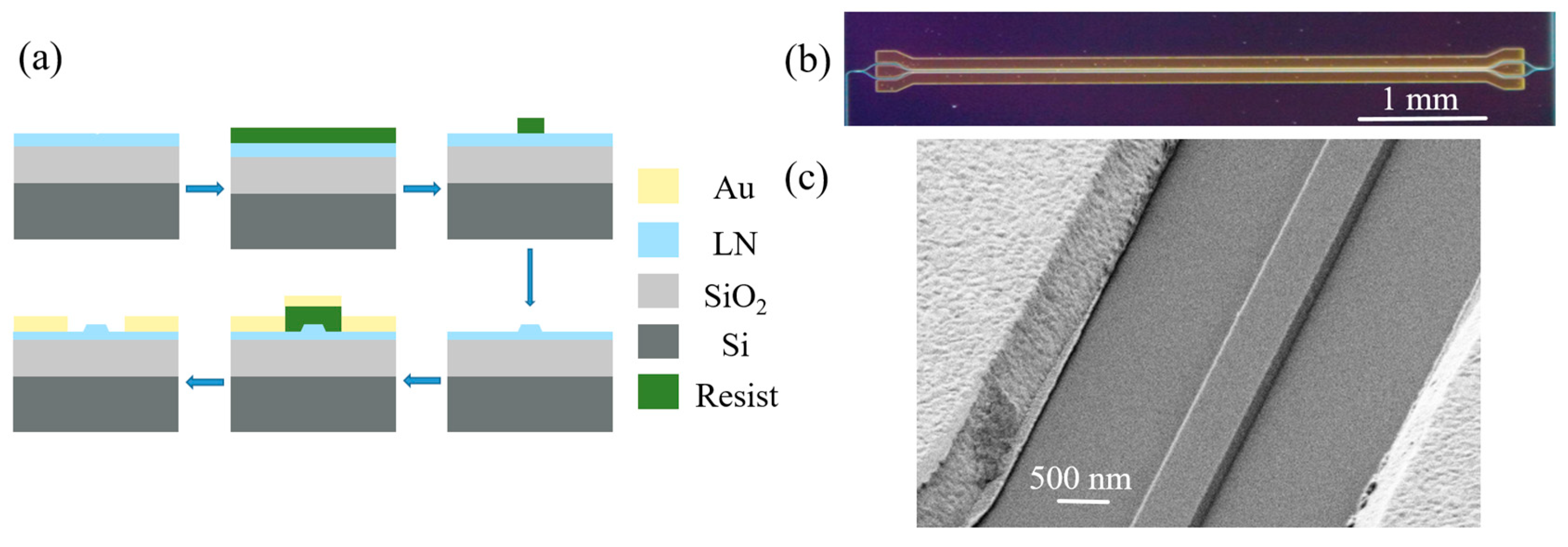
The fabrication process of EOM is shown in Figure 4a. A layer of electron-beam resist is spin-coated on the TFLN surface, and the MZI pattern is defined by electron-beam lithography and transferred to the LN layer by argon plasma etching using an ICP-RIE system (Oxford Instruments PlasmaPro100 Cobra, Oxford, UK). The LN waveguides are etched using an argon flow of 15 sccm, an RF power of 50 W, an ICP power of 1000 W, and a chamber pressure of 2 mTorr. The etching rate is approximately 0.4 nm/s. For the target etching depth of 150 nm, the corresponding etching time is approximately 375 s, allowing precise control of the waveguide depth and profile. After resist removal, a photolithography process is performed to define the electrode patterns. A gold film is deposited by thermal evaporation at a rate of 2–3 Å/s under a chamber pressure of 1 × 10⁻⁴ Pa, while the substrate temperature is maintained at 20 °C. The metal electrodes are finally patterned by a lift-off process. After the lift-off process, the Au electrode thickness is measured using a profilometer and is found to be approximately 500 nm. Figure 4b,c show the optical microscope image of the fabricated device and the SEM image of the modulation region, respectively.
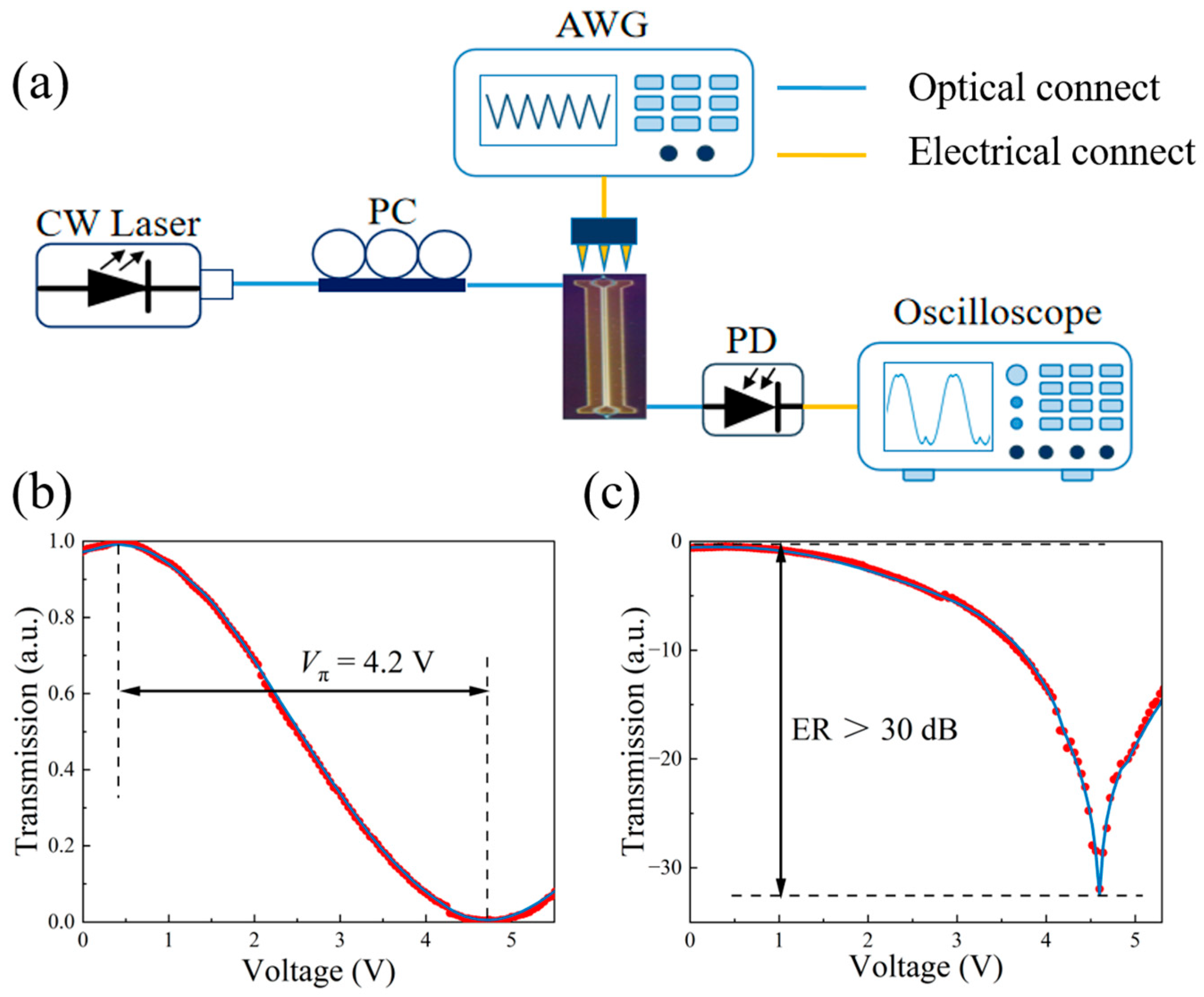
To evaluate the modulation efficiency of the fabricated EOM, a 50 kHz triangular electrical signal generated from an arbitrary waveform generator (AWG) is applied to the electrode via a RF probe. The modulated optical signal at 1064 nm is detected by a photodetector and its response is recorded by an oscilloscope as shown in Figure 5a. The normalized modulated waveform is presented in Figure 5b. A half-wave voltage Vπ of 4.2 V is extracted and the corresponding voltage-length product is 2.1 V·cm. By measuring the maximum and minimum light intensity, we obtain an ER exceeding 30 dB shown in Figure 5c. The total fiber-to-fiber optical insertion loss of the fabricated device is directly measured to be 14.8 dB, including both input/output coupling losses and on-chip propagation loss. To the best of our knowledge, this extinction ratio is the highest among the reported 1064 nm TFLN electro-optic modulators [5,18,19,20,21]. Such high ER indicates that the performances of the fabricated optical components, i.e., MMI coupler and single-mode waveguide, are consistent with our simulations and the fabrication quality is high.
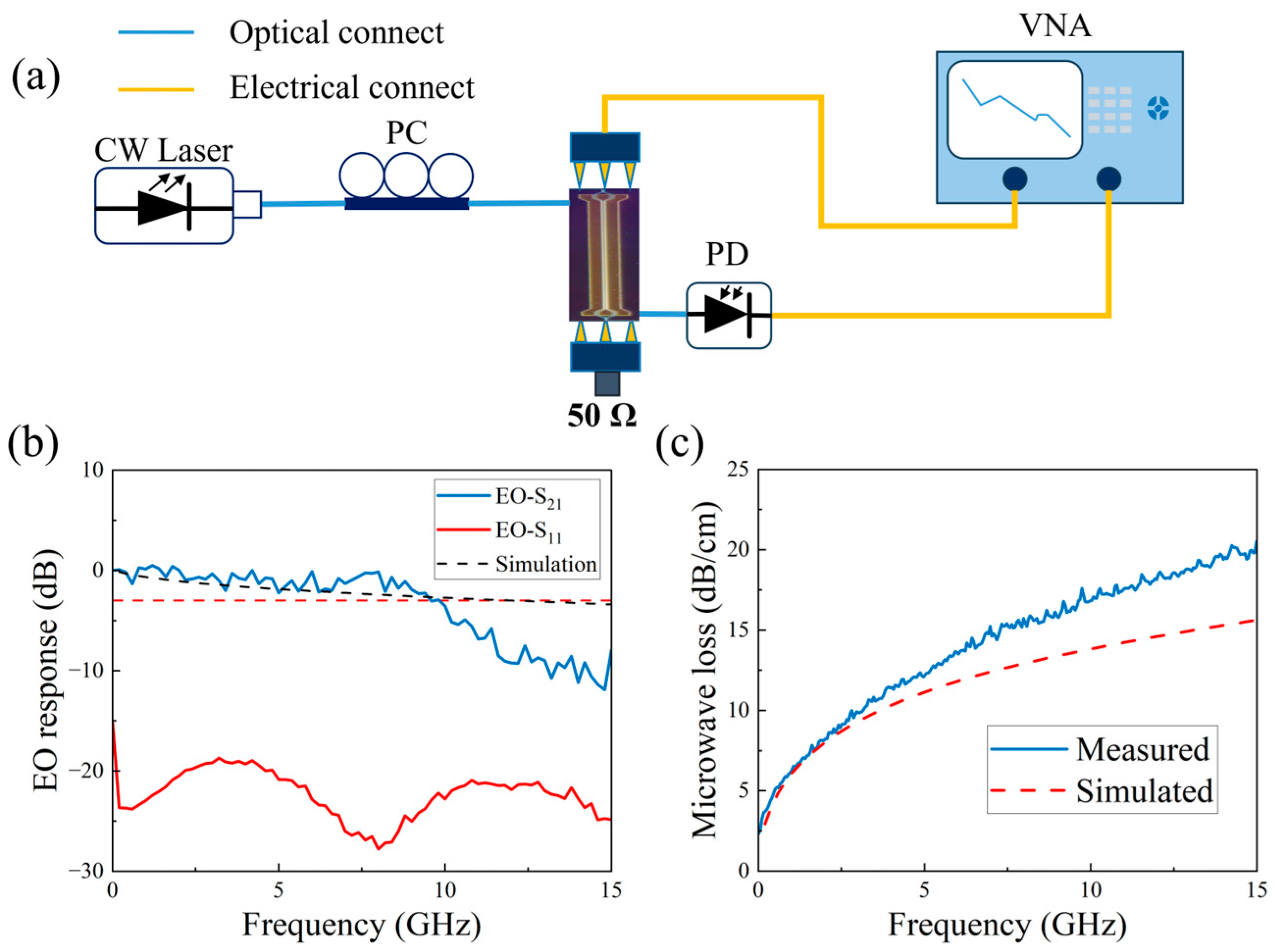
The modulation bandwidth is also characterized as shown in Figure 6a. The traveling-wave electrode is terminated by a standard 50 Ω load for impedance matching. A vector network analyzer with a frequency range from 100 MHz to 40 GHz is used to measure the EO response of the EOM (S21) and the electrical reflection coefficient S11. The measured results shown in Figure 6b indicate that the 3 dB bandwidth of the modulator exceeds 10 GHz. The EO S11 curve shows low RF reflection (<−15 dB) up to 15 GHz. The lower measured bandwidth compared with the simulated result is likely due to non-ideal electrode properties such as surface roughness and variations in conductivity. To evaluate this effect, the measured metal conductivity and microwave loss are incorporated into the simulation. The metal conductivity is measured to be 6 × 10⁶ S/m by the four-probe DC method, which is 7 times lower than the theoretical value [32]. The measured microwave loss and the simulated one considering the measured conductivity are shown in Figure 6c. Their discrepancy can be probably attributed to the surface roughness. Taking into account the measured conductivity and microwave loss in the simulation of the bandwidth (black dashed line in Figure 6b), we find better agreement with the measured bandwidth, indicating that electrode quality is a key factor affecting bandwidth performance. The bandwidth performance can be further improved by optimizing the electrode design and improving the fabrication quality of the electrode.

4. Discussion

Table 1 summarizes the key performance parameters of recently reported TFLN EOMs operating at 1064 nm [5,18,19,20,21]. It can be seen that the extinction ratio of the proposed device exceeds 30 dB, reaching the highest among the reported counterparts at the same wavelength. This high extinction ratio confirms that the fabricated MMI coupler and single-mode waveguides meet the design requirements, and the optical performances of the components are consistent with our simulation expectations. Furthermore, to evaluate the reproducibility of the fabricated devices, we measure four nominally identical modulators. The extinction ratios of all devices are consistently high, ranging from 28 dB to 32 dB, indicating good device-to-device reproducibility. Comprehensive comparison indicates that benefiting from the ultra-high extinction ratio, compact device footprint and superior fabrication reproducibility, the proposed modulator possesses distinct advantages and great application potential in scenarios requiring high optical signal contrast.

5. Conclusions

In conclusion, we demonstrate an EOM on TFLN working at 1064 nm. High-extinction-ratio MZI is proposed by designing a single-mode waveguide and a MMI coupler with a splitting ratio of 50:50. The fabricated device exhibits a voltage-length product of 2.1 V·cm, an EO bandwidth exceeding 10 GHz and a high extinction ratio of over 30 dB. This represents the highest ER reported for 1064 nm modulators on TFLN to date. Such a high-extinction-ratio EOM is believed to play a key role in the applications of quantum photonics, long-range BOTDR sensing system, integrated optical switches, and microwave photonics. Although this work focuses on small-signal EO modulation performance, 1064 nm is sometimes used with relatively high-power lasers and may lead to practical issues for some applications. At high optical powers, photorefractive effects in LN waveguides may induce refractive-index variations and bias drift, thereby affecting the extinction ratio and modulation stability. Future work will investigate the optical-power-dependent and long-term stability of the device and explore mitigation strategies, such as material doping and thermal management, to ensure reliable high-power operation [33].

Author Contributions

Conceptualization, Z.S. and L.C.; methodology, Z.S. and L.C.; investigation, Z.S.; formal analysis, Z.S.; validation, Z.S.; data curation, Z.S.; resources, L.C.; writing—original draft preparation, Z.S.; writing—review and editing, L.C.; supervision and L.C. All authors have read and agreed to the published version of the manuscript.

Funding

This research received no external funding.

Institutional Review Board Statement

Not applicable.

Informed Consent Statement

Not applicable.

Data Availability Statement

The original contributions presented in this study are included in the article. Further inquiries can be directed to the corresponding author.

Conflicts of Interest

The authors declare no conflicts of interest.

References

  1. Chen, Q.; Mao, S.; Yin, Z.; Yi, Y.; Li, X.; Wang, A.; Wang, X. Compact and efficient 1064 nm up-conversion atmospheric lidar. Opt. Express 2023, 31, 23931–23943. [Google Scholar] [CrossRef]
  2. Wang, A.; Yin, Z.; Mao, S.; Wang, L.; Yi, Y.; Chen, Q.; Müller, D.; Wang, X. Measurements of particle extinction coefficients at 1064 nm with lidar: Temperature dependence of rotational Raman channels. Opt. Express 2024, 32, 4650–4667. [Google Scholar] [CrossRef]
  3. Wang, L.; Yin, Z.; Lu, T.; Yi, Y.; Dong, X.; Dai, Y.; Bu, Z.; Chen, Y.; Wang, X. 1064 nm rotational Raman polarization lidar for profiling aerosol and cloud characteristics. Opt. Express 2024, 32, 14963–14977. [Google Scholar] [CrossRef]
  4. Pauly, R.M.; Yorks, J.E.; Hlavka, D.L.; McGill, M.J.; Amiridis, V.; Palm, S.P.; Rodier, S.D.; Vaughan, M.A.; Selmer, P.A.; Kupchock, A.W.; et al. A Cloud-Aerosol Transport System (CATS) 1064 nm calibration and validation. Atmos. Meas. Tech. 2019, 12, 6241–6258. [Google Scholar] [CrossRef] [PubMed]
  5. Kincaid, P.S.; Pruiti, N.G.; De Marinis, L.; Sorel, M.; Contestabile, G.; Andriolli, N. Waveguide design for a TFLN platform at 1064 nm for applications in spacecom and spectroscopy. Sci. Rep. 2026, 16, 1930. [Google Scholar] [CrossRef]
  6. Reed, G.T.; Mashanovich, G.; Gardes, F.Y.; Thomson, D. Silicon optical modulators. Nat. Photonics 2010, 4, 518–526. [Google Scholar] [CrossRef]
  7. Hu, Y.; Zhu, D.; Lu, S.; Zhu, X.; Song, Y.; Renaud, D.; Assumpcao, D.; Cheng, R.; Xin, C.J.; Yeh, M.; et al. Integrated electro-optics on thin-film lithium niobate. Nat. Rev. Phys. 2025, 7, 237–254. [Google Scholar] [CrossRef]
  8. Xie, Z.; Bo, F.; Lin, J.; Hu, H.; Cai, X.; Tian, X.-H.; Fang, Z.; Chen, J.; Wang, M.; Chen, F.; et al. Recent development in integrated lithium niobate photonics. Adv. Phys. X 2024, 9, 2322739. [Google Scholar] [CrossRef]
  9. Wang, C.; Zhang, M.; Chen, X.; Bertrand, M.; Shams-Ansari, A.; Chandrasekhar, S.; Winzer, P.; Lončar, M. Integrated lithium niobate electro-optic modulators operating at CMOS-compatible voltages. Nature 2018, 562, 101–104. [Google Scholar] [CrossRef]
  10. He, M.; Xu, M.; Ren, Y.; Jian, J.; Ruan, Z.; Xu, Y.; Gao, S.; Sun, S.; Wen, X.; Zhou, L.; et al. High-performance hybrid silicon and lithium niobate Mach–Zehnder modulators for 100 Gbit/s and beyond. Nat. Photonics 2019, 13, 359–364. [Google Scholar] [CrossRef]
  11. Kharel, P.; Reimer, C.; Luke, K.; He, L.; Zhang, M. Breaking voltage–bandwidth limits in integrated lithium niobate modulators using micro-structured electrodes. Optica 2021, 8, 357–363. [Google Scholar] [CrossRef]
  12. Chen, N.; Lou, K.; Yu, Y.; He, X.; Chu, T. High-efficiency electro-optic modulator on thin-film lithium niobate with high-permittivity cladding. Laser Photonics Rev. 2023, 17, 2200927. [Google Scholar] [CrossRef]
  13. Feng, H.; Zhang, K.; Sun, W.; Ren, Y.; Zhang, Y.; Zhang, W.; Wang, C. Ultra-high-linearity integrated lithium niobate electro-optic modulators. Photonics Res. 2022, 10, 2366–2373. [Google Scholar] [CrossRef]
  14. Meng, X.; Yuan, C.; Cheng, X.; Yuan, S.; Shang, C.; Pan, A.; Qu, Z.; Wang, X.; Wang, J.; Zhang, P.; et al. Thin-film lithium niobate modulators with ultra-high modulation efficiency. Laser Photonics Rev. 2025, 19, 2400809. [Google Scholar] [CrossRef]
  15. Tang, Y.; Li, H.; Chen, Q.; Dai, X.; Xia, J.; Lu, Q.; Huang, L.; Guo, W. High performance thin-film lithium niobate modulator with suppressed slot-line mode on quartz substrate fabricated by photolithography. J. Light. Technol. 2025, 43, 636–647. [Google Scholar] [CrossRef]
  16. Liu, H.; He, Y.; Xiong, B.; Sun, C.; Hao, Z.; Wang, L.; Wang, J.; Han, Y.; Li, H.; Gan, L.; et al. Ultrahigh-efficiency dual-band thin-film lithium niobate modulator incorporating low-k underfill for 390 Gbit/s PAM8 transmission. Laser Photonics Rev. 2025, 19, 2402053. [Google Scholar] [CrossRef]
  17. Zhang, J.; Shen, J.; Wang, S.; Li, Z.; Yue, W.; Ou, X.; Cai, Y. 512 Gbps/λ dual-polarization thin-film lithium niobate modulators based on an electro-optic equalizer. Nanophotonics 2025, 14, 4783–4792. [Google Scholar] [CrossRef] [PubMed]
  18. Jagatpal, N.; Mercante, A.J.; Ahmed, A.N.R.; Prather, D.W. Thin film lithium niobate electro-optic modulator for 1064 nm wavelength. IEEE Photonics Technol. Lett. 2021, 33, 271–274. [Google Scholar] [CrossRef]
  19. Yan, H.; Pan, B.; Xie, Y.; Liu, L.; Zhi, L.; Dai, D. Thin-film lithium-niobate-on-insulator modulators at a wavelength of 1064 nm for high-power applications. In Proceedings of the 2023 Opto-Electronics and Communications Conference (OECC 2023), Shanghai, China, 2–6 July 2023; pp. 1–3. [Google Scholar] [CrossRef]
  20. Zhang, B.; Qu, J.; Weng, Y.; Jiang, W.; Du, J.; Chen, X.; Zhou, L. High-bandwidth CMOS-level integrated thin-film lithium niobate electro-optic modulator at 1064 nm wavelength. Opt. Laser Technol. 2025, 191, 113335. [Google Scholar] [CrossRef]
  21. Moller de Freitas, M.; Zhu, X.; Isti, M.I.; Arnold, J.; Xue, R.; Zhang, J.; Yao, P.; Creazzo, T.; Cullen, C.; Shi, S.; et al. Thin-Film Lithium Niobate MZM Operating at 1-µm Wavelength with Low Vπ and High Bandwidth. IEEE Photonics Technol. Lett. 2026, 38, 555–558. [Google Scholar] [CrossRef]
  22. Xie, S.; Veilleux, S.; Dagenais, M. On-chip high extinction ratio single-stage Mach–Zehnder interferometer based on multimode interferometer. IEEE Photonics J. 2022, 14, 1–6. [Google Scholar] [CrossRef]
  23. Wang, Z.; Xiang, M.; Yang, F.; Liu, K.; Bao, J.; Yang, D.; Wang, Y. Ultrafast and high extinction ratio 1×4 electro-optical switch based on cascaded dual-output MZI. IEEE Photonics J. 2023, 15, 6601008. [Google Scholar] [CrossRef]
  24. Kanno, A.; Honda, S.; Yamanaka, R.; Sotobayashi, H.; Kawanishi, T. Ultrafast and broadband frequency chirp signal generation using a high-extinction-ratio optical modulator. Opt. Lett. 2010, 35, 4160–4162. [Google Scholar] [CrossRef]
  25. Cheng, Z.; Shu, X.; Ma, L.; Chen, B.; Li, C.; Sun, C.; Wei, M.; Yu, S.; Li, L.; Lin, H.; et al. On-chip silicon electro-optical modulator with ultra-high extinction ratio for fiber-optic distributed acoustic sensing. Nat. Commun. 2023, 14, 7409. [Google Scholar] [CrossRef] [PubMed]
  26. Lu, Y.; Yao, Y.; Zhao, X.; Wang, F.; Zhang, X. Influence of non-perfect extinction ratio of electro-optic modulator on signal-to-noise ratio of BOTDR. Opt. Commun. 2013, 297, 48–54. [Google Scholar] [CrossRef]
  27. Xu, Y.; Tian, Z.; Meng, X.; Chai, Z. Methods and applications of on-chip beam splitting: A review. Front. Phys. 2022, 10, 985208. [Google Scholar] [CrossRef]
  28. Jundt, D.H. Temperature-dependent Sellmeier equation for the index of refraction, ne, in congruent lithium niobate. Opt. Lett. 1997, 22, 1553–1555. [Google Scholar] [CrossRef]
  29. Olmon, R.L.; Slovick, B.; Johnson, T.W.; Shelton, D.; Oh, S.-H.; Boreman, G.D.; Raschke, M.B. Optical dielectric function of gold. Phys. Rev. B 2012, 86, 235147. [Google Scholar] [CrossRef]
  30. Lee, C.; Choi, H.; Jin, J.; Cha, M. Measurement of refractive index dispersion of a fused silica plate using Fabry-Perot interference. Appl. Opt. 2016, 55, 6285–6291. [Google Scholar] [CrossRef]
  31. El-Zaiat, E.Y.; Youssef, G.M. Dispersive parameters for complex refractive index of p- and n-type silicon from spectrophotometric measurements in spectral range 200–2500 nm. Opt. Laser Technol. 2015, 65, 106–112. [Google Scholar] [CrossRef]
  32. Gilani, T.H.; Rabchuk, D. Electrical resistivity of gold thin film as a function of film thickness. Can. J. Phys. 2017, 96, 272–274. [Google Scholar] [CrossRef]
  33. Kong, Y.; Bo, F.; Wang, W.; Zheng, D.; Liu, H.; Zhang, G.; Rupp, R.; Xu, J. Recent Progress in Lithium Niobate: Optical Damage, Defect Simulation, and On-Chip Devices. Adv. Mater. 2020, 32, 1806452. [Google Scholar] [CrossRef] [PubMed]
Figure 1. (a) Schematic of the Mach-Zehnder electro-optic modulator. (b) Cross-sectional schematic of the TFLN waveguide and CPW electrodes, showing the material stack and key geometric parameters.
Photonics 13 00505 g001
Figure 2. (a) Transmission of one output branch of the MMI coupler as a function of wavelength around 1064 nm. The red circle highlights the operating wavelength of 1064 nm, and the inset indicated by the red arrow shows the corresponding simulated optical field distribution. The other inset shows the geometry of the designed MMI. (b) Variation in effective refractive indices of different modes with waveguide top width. The grey dashed line indicates the selected waveguide top width of 600 nm.
Photonics 13 00505 g002
Figure 3. (a) Simulated half-wave voltage–length product (VπL) and metal-absorption-induced optical loss as a function of the electrode gap, g (wtop = 600 nm). The black curve (left arrow) corresponds to the optical loss, and the blue curve (right arrow) corresponds to the VπL. (b) Simulated electro-optic (EO) response of the modulator; the red line indicates the −3 dB level used to extract the EO 3 dB bandwidth.
Photonics 13 00505 g003
Figure 4. (a) Simplified schematic of the fabrication process flow for the TFLN modulator. (b) Optical microscope image of a fabricated device. (c) Scanning electron microscope (SEM) image of the fabricated EOM modulation region.
Photonics 13 00505 g004
Figure 5. (a) Experimental set-up for measuring the half-wave voltage Vπ and extinction ratio. AWG, Arbitrary Waveform Generator; PD, photodetector; PC, polarization controller. (b) Normalized optical transmission of the EOM on TFLN as a function of the applied voltage Vπ is extracted to be 4.2 V. (c) Normalized extinction ratio (ER) of over 30 dB on a logarithmic scale. The red dots represent the measured data points, and the blue curves are the corresponding fitted curves.
Photonics 13 00505 g005
Figure 6. (a) Schematic of the measurement setup; (b) Measured electro-optic transfer function S21 and electrical reflection coefficient S11 as a function of frequency; the red dashed line marks the −3 dB level for determining the EO 3 dB bandwidth; the black dashed line represents the simulated EO S21 response using the measured electrode conductivity. (c) Measured and simulated microwave loss of the device as a function of frequency.
Photonics 13 00505 g006
Table 1. Summary of key performance parameters of 1064 nm TFLN electro-optic modulators reported in recent studies.
ReferencesVπL (V·cm)3 dB Bandwidth (GHz) Extinction Ratio (dB)Modulation Length (mm)Insertion Loss (dB)Measurement Type
2021 [18]1.91--720Experimental
2023 [19]1.92>5-35Experimental
2025 [20]1.43810519Experimental
2025 [5]≈2.5 1----Simulation
2026 [21]1.454021.71012.64 2Experimental
This work2.1>10>30514.8Experimental
1 The reported value corresponds to a simulated single-arm phase shifter based on an etched TFLN waveguide. 2 Insertion loss corresponds to the reported total coupling loss; fiber-to-fiber insertion loss not explicitly reported.
Disclaimer/Publisher’s Note: The statements, opinions and data contained in all publications are solely those of the individual author(s) and contributor(s) and not of MDPI and/or the editor(s). MDPI and/or the editor(s) disclaim responsibility for any injury to people or property resulting from any ideas, methods, instructions or products referred to in the content.