
Article

MOCVD Regrowth and Surface Morphology Study of Distributed Bragg Reflector Structures on Photonic Crystal Layers


1
College of Electronics and Information Engineering, Sichuan University, Chengdu 610064, China
2
Suzhou Everbright Photonics Co., Ltd., Suzhou 215163, China
3
Jiangsu Key Laboratory of Semiconductor Laser and Sensing Technology, Suzhou 215163, China
4
College of Advanced Interdisciplinary Studies, National University of Defense Technology, Changsha 410073, China
5
Southeast University-Monash University Joint Graduate School (Suzhou), Southeast University, Suzhou 215125, China
*
Author to whom correspondence should be addressed.
Photonics 2026, 13(3), 262; https://doi.org/10.3390/photonics13030262
Submission received: 2 February 2026 / Revised: 3 March 2026 / Accepted: 6 March 2026 / Published: 10 March 2026
(This article belongs to the Special Issue Technologies of Laser Wireless Power Transmission)

Abstract

Photonic-crystal surface-emitting lasers (PCSELs) are a new type of semiconductor laser with the potential for high-power output and high-beam-quality operation. Integrating a distributed Bragg reflector (DBR) into PCSELs can significantly enhance device performance. However, the growth of high-aluminum-content DBRs on photonic crystal layers with buried air holes presents two major challenges. First, the low mobility of aluminum atoms increases the propagation of surface roughness from the substrate into the DBR, increasing defect density. Second, the high growth temperatures required for DBR growth can deform the thermally unstable air holes. In this work, we investigated a metal–organic chemical vapor deposition (MOCVD) regrowth process for fabricating DBRs on PCSELs. By adjusting the epitaxial growth temperature and V/III ratio, we effectively controlled the diffusion of adatoms on both the sample surface and inside the holes. As a result, the root mean square (RMS) surface roughness decreased by ~96%, and uniform buried air holes were obtained, with a filling factor of ~ 18.8% and a depth of ~ 270 nm, without significant deformation. Finally, we fabricated a PCSEL device with a DBR structure, exhibiting a beam divergence angle of ~ 0.5° and a peak power of about 0.86 W. This study provides a key process solution for the development of PCSELs with high-quality DBR structures, enabling further improvement in optical output performance.

1. Introduction

There is a growing demand for high-power and high-brightness semiconductor lasers in various applications, such as material processing [1], bioimaging [2], and LiDAR systems [3,4]. For high-performance LiDAR, a pulsed laser source with high peak power and narrow beam divergence is essential to achieve long-distance and high-spatial-resolution ranging. Currently, most LiDAR systems primarily employ edge-emitting lasers (EELs) and vertical-cavity surface-emitting lasers (VCSELs) as light sources [5]. These lasers have the advantage of high power and high electro-optical conversion efficiency [6,7,8]. However, their use in direct semiconductor applications is limited due to large beam divergence and poor beam quality [9,10]. As a result, extensive optical components are often required for optical shaping, which introduces challenges in system integration, stability, and cost. Photonic-crystal surface-emitting lasers (PCSELs) [11,12,13] have shown great potential to overcome these limitations. PCSELs achieve laser oscillation through two-dimensional standing waves at singular points (Γ, M, and so on) of the photonic crystal band structure. Because of their ability to maintain such two-dimensional coherent resonance over a large area, they can deliver nearly diffraction-limited beam output, making them promising candidates for high output power and beam quality operation [14].
However, a limitation of PCSELs is that the photonic crystal (PC) radiates simultaneously towards the p-side and the n-side. The emission towards the p-side is partially absorbed by the p-side electrode, leading to optical loss and reduced slope efficiency. Previous studies have shown that introducing a distributed Bragg reflector (DBR) [15,16,17] can effectively enhance the slope efficiency by reflecting more of the light diffracted towards the p-side back towards the n-side. This approach also reduces the injection current, energy consumption, and device heating [18,19]. When constructive interference occurs between the reflected light and the upward radiation, the slope efficiency can be nearly doubled compared to equivalent devices without a DBR, thereby maximizing the output [11]. Additionally, a highly reflective DBR can suppress the direct nonuniform reflection effect from the p-side electrode, resulting in a narrower beam divergence angle [20]. In 2021, the Noda group in Japan [20] successfully demonstrated a PCSEL device incorporating a DBR structure, achieving a high peak power of 10 W. The device maintained an ultra-narrow beam divergence angle of approximately 0.1° (FWHM) within a 500 µm diameter resonator, making it well-suited for LiDAR applications. Therefore, growing a high-quality DBR structure on a photonic crystal layer with buried air holes is of great significance, as it can significantly improve both the output power and beam quality of PCSEL devices. Currently, the influence of epitaxial growth conditions on the morphology of DBR structures in PCSELs has not been systematically studied. We employed metal–organic chemical vapor deposition (MOCVD) to introduce a p-type DBR structure consisting of forty pairs of Al0.06GaAs/Al0.9GaAs into the PCSEL, aiming to realize high-output-performance devices.
There are two key challenges when introducing a p-type DBR into a PCSEL. First, during MOCVD growth of DBR layers on photonic crystal substrates with buried air holes, surface roughness from the substrate tends to propagate into the DBR layers. This propagation disrupts the flatness of the interfaces, increases optical scattering losses, and significantly reduces the reflectivity of the DBR [21,22]. The second is that the growth temperature of DBR is limited. Elevated temperatures lower the migration barrier for adatoms inside the air holes, increasing their diffusion length and eventually causing hole deformation [23]. Scattering loss in the DBR primarily stems from surface roughness, which results from the low surface mobility of aluminum atoms during the growth of high-aluminum-content DBRs on patterned substrates. This low mobility tends to promote three-dimensional island growth, disrupting the flatness of each layer interface. As this roughness accumulates layer by layer, it amplifies the structural imperfections and ultimately damages the overall surface morphology [24]. Both the DBR and the buried air holes are highly sensitive to growth temperature. Typically, p-type Al0.42GaAs cladding layers grown at 580–650 °C result in well-defined buried air holes [25,26,27]. In contrast, the growth of high-aluminum-content DBRs requires elevated temperatures—typically around 700 °C [28]—to enhance aluminum atom mobility and ensure high-quality layer formation. However, once the air holes are buried, increasing the temperature during the growth of DBR increases the mobility of atoms in the air holes, which can easily lead to deformation of the air holes.
In this work, we address the aforementioned challenges by optimizing the DBR epitaxial growth conditions. Specifically, we employ a low-temperature, low V/III ratio growth regime. The reduced temperature suppresses adatom diffusion inside the holes, helping to preserve the morphology of the buried air holes, while the low V/III ratio promotes aluminum atom diffusion across the wafer surface, thereby improving the quality of the DBR interfaces. As a result, we achieved a root mean square (RMS) surface roughness of only 0.672 nm in the patterned region of the sample and obtained uniform buried air holes with a filling factor of ~18.8% (defined as the ratio of hole area to total unit cell area) [29] and a depth of ~270 nm. The filling factor was calculated at the position where the air hole reached its maximum width at the bottom. This demonstrates that a high-quality DBR structure can be realized while maintaining the structural integrity of the buried air holes. Finally, the fabricated PCSEL device exhibited a beam divergence angle of approximately 0.5° and achieved a peak power of around 0.86 W under an injection current of 10 A.

2. Experiment

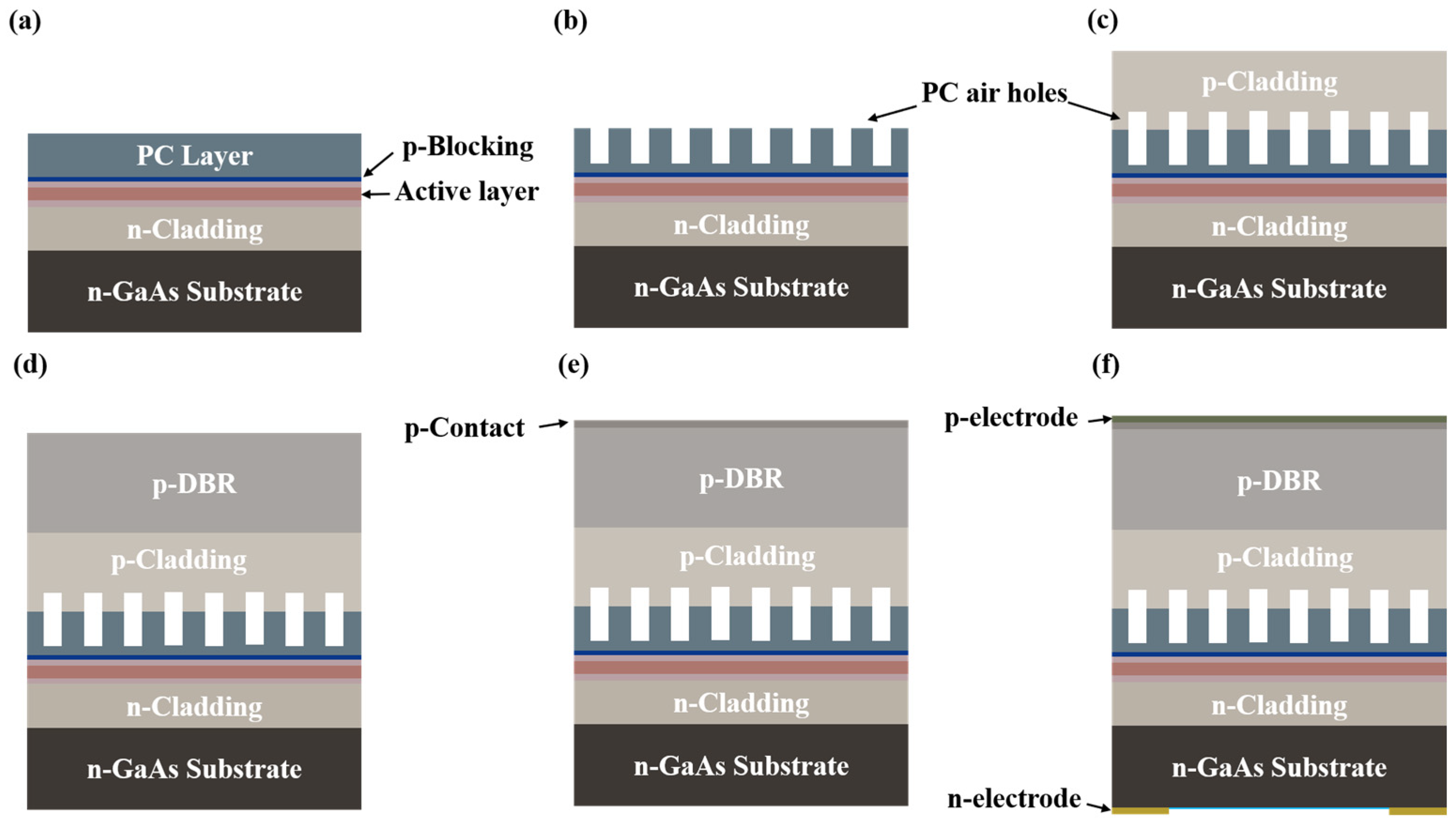
The fabrication process of the PCSEL device is illustrated in Figure 1, where epitaxial growth serves as one of the core steps. The epitaxial structure was grown on an n-type GaAs substrate using MOCVD. Trimethylindium (TMIn), trimethylgallium (TMGa), and trimethylaluminum (TMAl) were used as group-III precursors, while arsine (AsH3) and phosphine (PH3) were used as group-V precursors. Carbon tetrabromide (CBr4) and disilane (Si2H6) were employed as the p-type and n-type dopant sources, respectively.
The initial growth structure consisted of an n-GaAs substrate, an n-Al0.69GaAs cladding layer, a waveguide layer, a multiple quantum well (MQW) active region, a p-Al0.5GaAs electron-blocking layer, and a p-GaAs photonic crystal layer. The active region comprised a three-period InGaAs/GaAsP MQW structure.
To form periodically arranged buried air holes, electron beam lithography (EBL) was first used to define isosceles right-triangle hole patterns on the GaAs layer. The length of the two perpendicular sides of each triangle was designed to be 200 nm, and the photonic crystal period was set to 277 nm, as shown in Figure 1b. The photonic crystal pattern was transferred into the GaAs layer using inductively coupled plasma (ICP) dry etching with a Cl2/BCl3/Ar gas mixture, which enables anisotropic etching with good sidewall definition. The patterned substrate was then returned to the MOCVD reactor for a continuous regrowth process carried out at a reactor pressure of 390 mbar. A p-type Al0.42GaAs cladding layer was first regrown, followed by high-temperature growth of a p-type DBR layer consisting of forty pairs of Al0.06GaAs/Al0.9GaAs materials. During this step, to prevent the p-type Al0.42GaAs cladding from filling the air holes and to suppress deformation of the holes during high-temperature DBR growth, we carefully adjusted the growth temperature and V/III ratio. These adjustments suppressed the diffusion of adatoms into the buried air holes, helping preserve their shape while promoting a smooth surface morphology for high-quality DBR formation. As a result, an epitaxial wafer with triangular buried air holes and a forty-pair DBR structure was successfully fabricated, completing the epitaxial growth process, as illustrated in Figure 1e.
Following the epitaxial regrowth, a mesa structure with a height of 0.5 μm was defined on the p-side of the wafer using mesa etching, followed by the deposition of the p-side electrode. Subsequently, an n-side electrode was fabricated on the n-side of the wafer using metal sputtering, thus completing the device fabrication process.

3. Results and Discussion

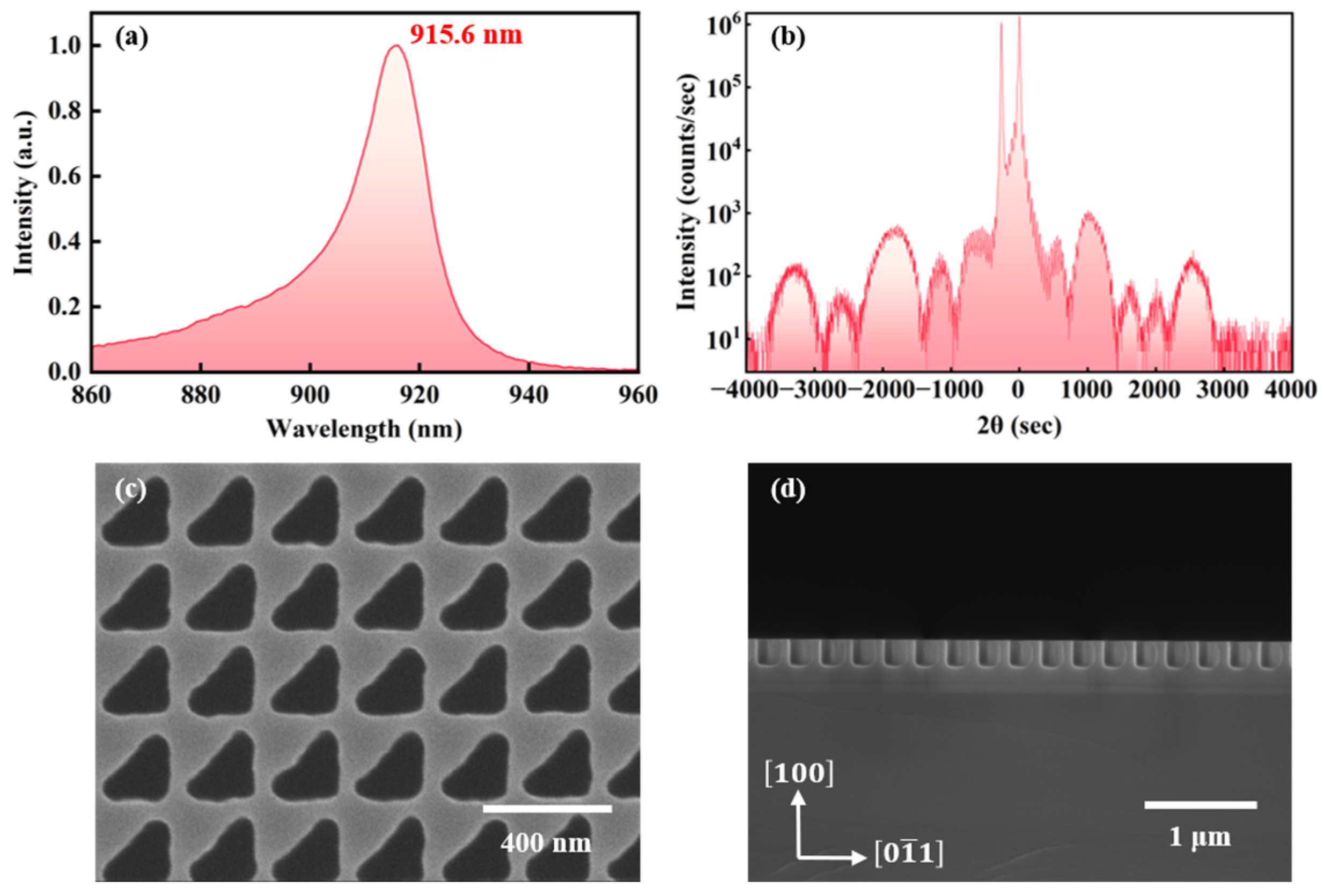
To better control the performance of the PCSEL, non-destructive characterization was performed at each key step of the fabrication process. High-resolution X-ray diffraction (HRXRD) and photoluminescence (PL) measurements were used to monitor the MQW structure, interface quality, layer thickness, and fluorescence emission spectrum of the epitaxial wafer. Figure 2a shows the PL spectrum of the MQW structure, with a peak wavelength and full width at half maximum (FWHM) of 915.6 nm and 16 nm, respectively. Figure 2b presents the HRXRD ω–2θ scan of the wafer. The presence of clear satellite peaks corresponding to multiple diffraction orders indicates good interface quality in the MQW. These measurements ensured that the epitaxial growth met the design specifications. In addition, scanning electron microscopy (SEM) was used to observe the morphology of the photonic crystal structure after electron beam lithography and dry etching, allowing us to monitor the etching profile of the air holes before the regrowth process and verify whether the photonic crystal structure conformed to the intended design. Figure 2c,d show SEM images of the air holes, which demonstrate good pattern fidelity and uniformity.
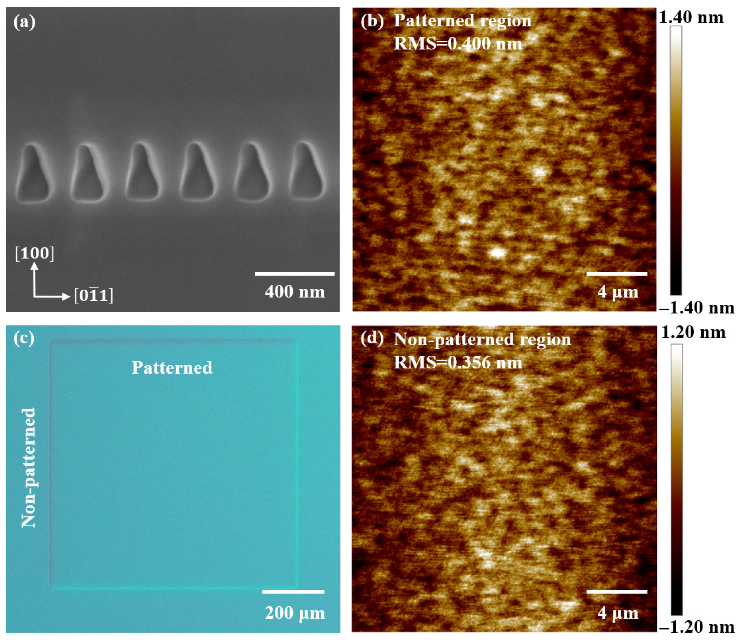
In the first stage, a triangular buried air hole PCSEL without a DBR structure was fabricated. During the experiment, critical growth parameters—including temperature, V/III ratio, and growth rate—were strictly controlled to maintain their target values. The p-type Al0.42GaAs cladding layer was grown at a temperature of 640 °C. As shown in Figure 3a, cross-sectional SEM analysis confirmed that the regrowth process successfully produced uniformly distributed buried air holes with a filling factor of approximately 17.7% and a hole depth of around 290 nm. Atomic force microscopy (AFM) was used to characterize the patterned region over a 20 μm × 20 μm scan area, revealing a root mean square (RMS) surface roughness of 0.400 nm, as shown in Figure 3b, indicating a relatively smooth surface. The RMS of the surface roughness was measured at the top of the cladding layer. Optical microscopy (OM) characterization of the regrown epitaxial surface showed that both the patterned and unpatterned areas remained relatively flat, as presented in Figure 3c. The AFM result for the unpatterned region, shown in Figure 3d, exhibited an RMS roughness of 0.356 nm over the same scan area. The RMS roughness in the photonic crystal region was approximately 11% higher than that in the unpatterned region, which can be attributed to the propagation of roughness from the photonic crystal layer into the DBR structure [24]. Further morphological analysis revealed that both the photonic crystal and non-photonic crystal regions exhibited three-dimensional island-like defects on the surface. As shown in Figure 3b,d, this surface morphology is related to the diffusion behavior of adatoms during the growth process [22]. These experimental results demonstrate that, without a DBR structure, the fabrication process successfully produced a high-quality epitaxial surface with uniformly distributed buried air holes.
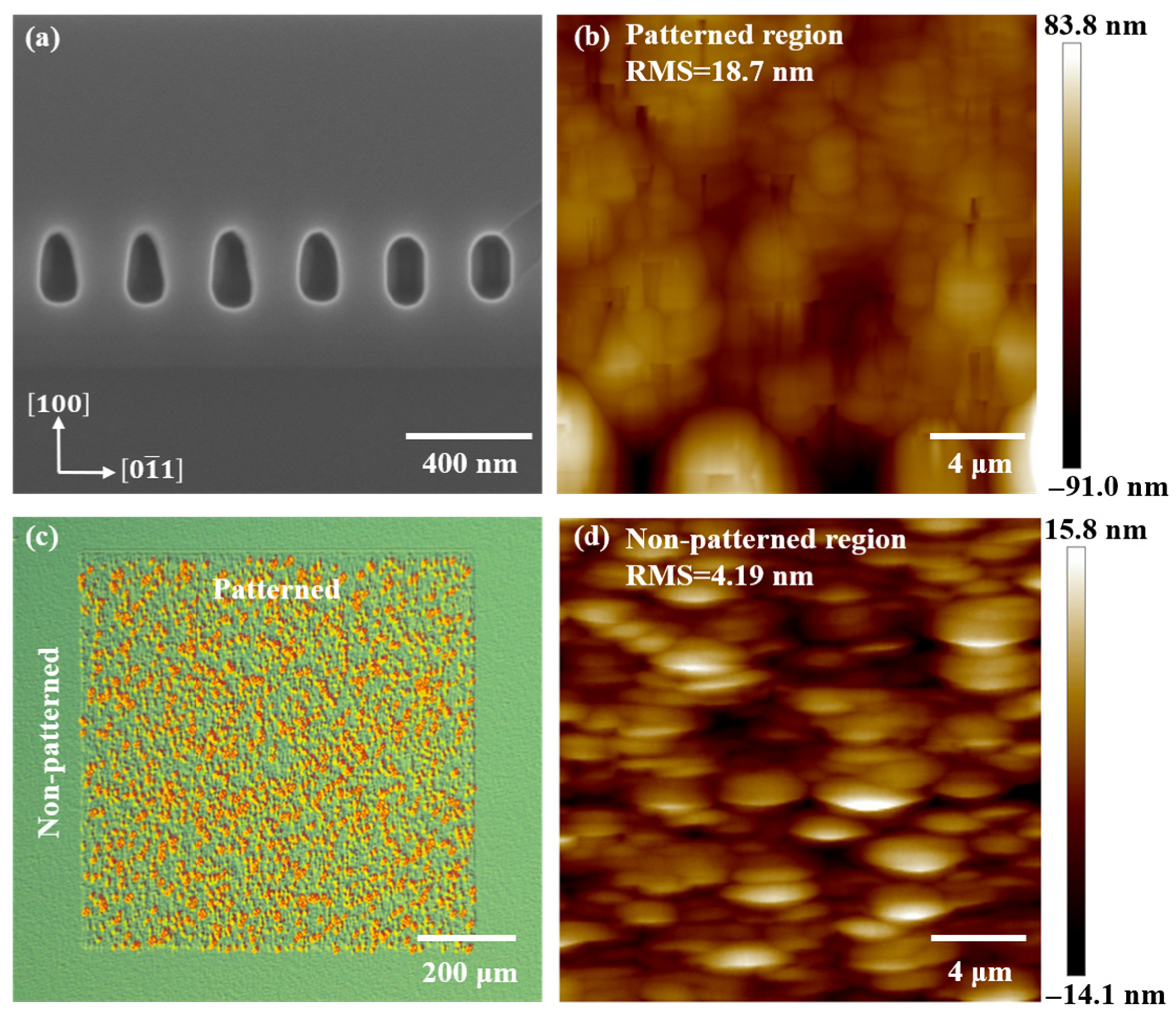
Based on the previously established growth conditions for the p-type Al0.42GaAs cladding layer, we next introduced a forty-pair Al0.06GaAs/Al0.9GaAs DBR structure to fabricate an epitaxial wafer incorporating a p-type DBR. The DBR layers were grown at a typical temperature of 700 °C, while the growth parameters of the p-type cladding were kept unchanged to preserve the morphology of the buried air holes. Cross-sectional SEM characterization of the regrown interface, as shown in Figure 4a, revealed that the morphological uniformity of the buried air holes was disrupted. The holes exhibited non-uniform sizes and became more symmetric in shape. The filling factor of the air holes at this stage was approximately 12.8%, with a depth of about 250 nm. Surface morphology analysis revealed a noticeable increase in surface defect density within the patterned region, while the unpatterned region exhibited significantly lower defect density, as shown in Figure 4c. Quantitative AFM measurements further confirmed these findings: the patterned region displayed an RMS roughness of 18.7 nm over a 20 μm × 20 μm area, whereas the unpatterned region showed an RMS roughness of 4.19 nm. The roughness in the patterned region increased by 77.6% compared to the unpatterned region, indicating substantial surface degradation, as illustrated in Figure 4b,d. The AFM image in Figure 4b reveals several rectangular pits on the surface of the patterned region. The AFM image of the non-patterned region in Figure 4d shows large, aggregated, three-dimensional island-like defects.
Through multidimensional characterization of the materials and structures, the data shown in Figure 4 were obtained. These results indicate that the previously established typical DBR growth condition of 700 °C is not suitable for DBR growth on a photonic crystal structure. As discussed earlier, the introduction of a p-type DBR in PCSELs involves an inherent conflict between the thermal instability of buried air holes and the high-temperature environment required for DBR growth. The results in Figure 4 directly confirm the difficulty and challenges in device fabrication arising from this contradiction.
First, as shown in the cross-sectional SEM image of the buried air holes in Figure 4a, comparison with the previous dataset without a DBR structure reveals that growing the DBR at 700 °C on the photonic crystal layer is equivalent to subjecting the buried air holes to prolonged high-temperature annealing. Consequently, the cross-sectional shape of the holes evolves toward a symmetric “circular” profile rather than the asymmetric “triangular” shape shown in Figure 3. This phenomenon can be explained from both thermodynamic and kinetic perspectives. The buried air holes consist of different crystallographic facets, which exhibit markedly different chemical properties and orientation-dependent growth kinetics, resulting in substantial variations in growth rates across the patterned region [30]. For example, during growth, material tends to migrate from sharp regions with higher chemical potential to regions with lower chemical potential. According to thermodynamic principles, this process ultimately minimizes the chemical potential of the structure and drives it toward the lowest-energy state [31]. These two factors determine the final morphology of the structure; by controlling growth conditions, the extent of mass transport—and thus the final structural shape—can be controlled. At 700 °C, atoms within the holes acquire sufficient thermal energy to overcome diffusion barriers and migrate from regions of higher chemical potential to regions of lower chemical potential. This process seeks to minimize the chemical potential and leads the structure toward a stable configuration with minimum energy, namely the nearly symmetric “circular” shape observed in Figure 4a.
Second, as shown in the OM and AFM images in Figure 4b–d, comparison with the previous dataset without a DBR structure indicates a high density of surface defects. On the one hand, the relatively weak As–Ga and As–Al bonds lead to arsenic desorption at high temperatures, resulting in pit formation as observed in the AFM images [23]. On the other hand, the surface morphology is strongly governed by the surface migration of group-III species. Under high V/III ratio growth conditions, the high As precursor flow produces an As-rich surface. Upon arrival at the surface, Al atoms rapidly bond with As, which suppresses the migration of group-III atoms and leads to the formation of dense surface defects [32,33].
Such a structure is not suitable for our PCSEL devices. The interfacial roughness of the DBR can cause optical scattering losses, and the non-uniform morphology of the air holes further exacerbates these losses [34]. In addition, symmetric holes may reduce radiation efficiency [35]. Based on the above analysis, we selected 640 °C as the epitaxial growth temperature for the DBR, which is consistent with the growth temperature of the p-type cladding layer. At this temperature, the buried air holes do not undergo significant deformation. To address the increase in surface roughness caused by the reduced Al migration at this lower temperature, we further decreased the V/III ratio to promote the surface migration of Al atoms, thereby ensuring the interface quality of the DBR.
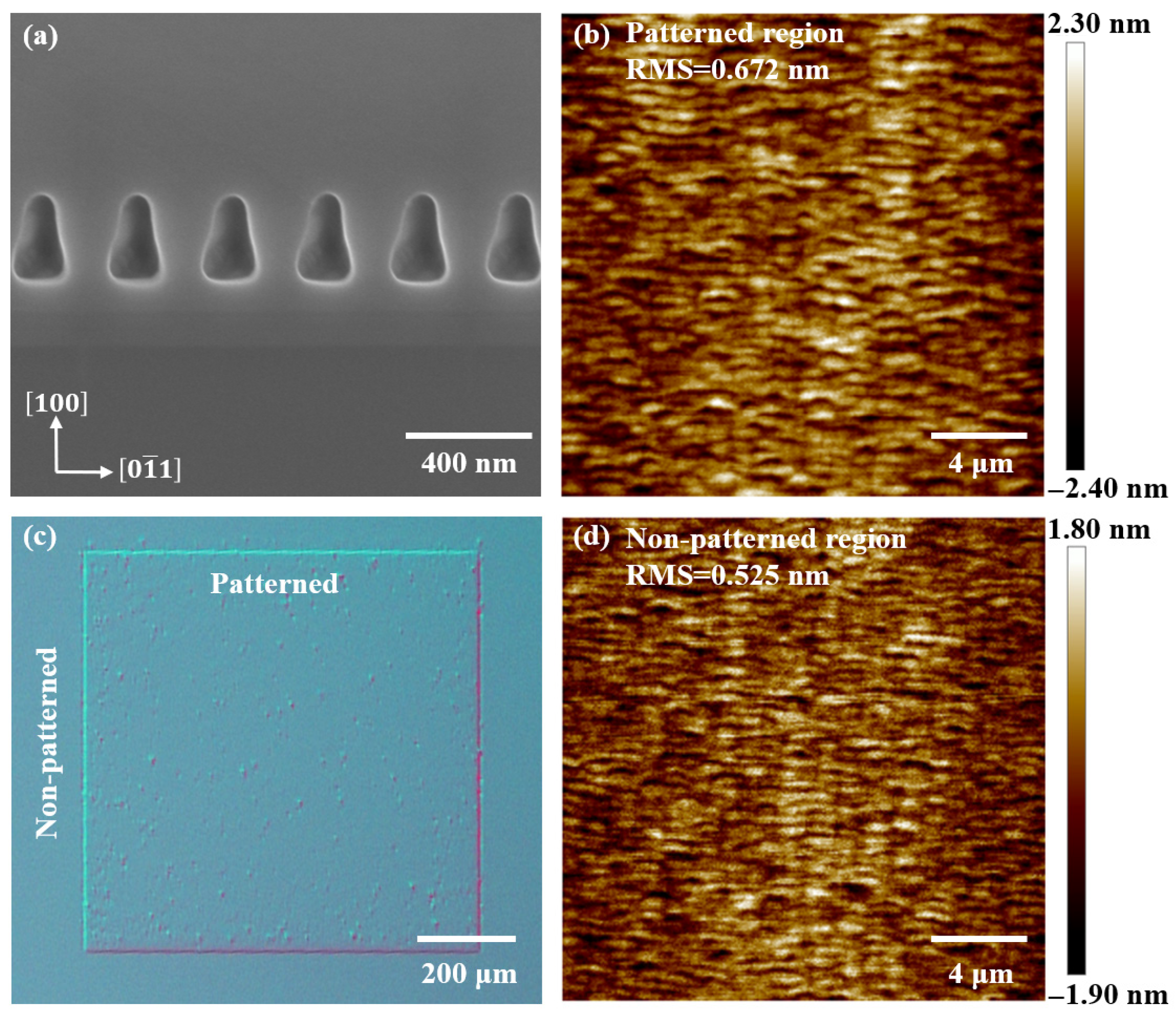
We adjusted the epitaxial growth conditions for the DBR to complete the PCSEL structure. Cross-sectional morphology analysis of the regrown region, shown in Figure 5a, revealed well-preserved and uniform buried air holes. At this stage, the filling factor was approximately 18.8%, and the hole depth was around 270 nm, indicating successful control over the hole morphology. Compared to the previous set of experiments, some crystallographic facets became visible on the holes, and the reduced radius of curvature at the top edge increased the sharpness. These changes are attributed to the reduced adatom mobility inside the holes due to the lower DBR growth temperature [36]. Compared to the structure without a DBR, the filling factor increased by 5.9%, while the hole depth decreased by about 20 nm. This indicates a morphology with reduced vertical and increased lateral dimensions, likely resulting from the extended total growth time introduced by the DBR layer [31]. Under optical microscopy, the surface particle density in the patterned region was significantly reduced compared to the unoptimized DBR process, and the surface morphology was markedly improved. The unpatterned region showed a smooth surface with no obvious defects, as shown in Figure 5c. Figure 5b,d present AFM results. Within a scan area of 20 μm × 20 μm, the patterned region exhibited an RMS surface roughness of 0.672 nm, while the unpatterned region showed an RMS roughness of 0.525 nm. The roughness in the patterned region was 21.9% higher than in the unpatterned region. By optimizing the regrowth conditions, the surface mobility of aluminum atoms was enhanced, leading to a significant reduction in three-dimensional island-like defects and an overall improvement in surface morphology [23]. Compared to the pre-optimized DBR growth, this process simultaneously achieved a high-quality DBR structure and a relatively large filling factor of the buried air holes, providing a key process foundation for the fabrication of high-performance PCSEL devices.
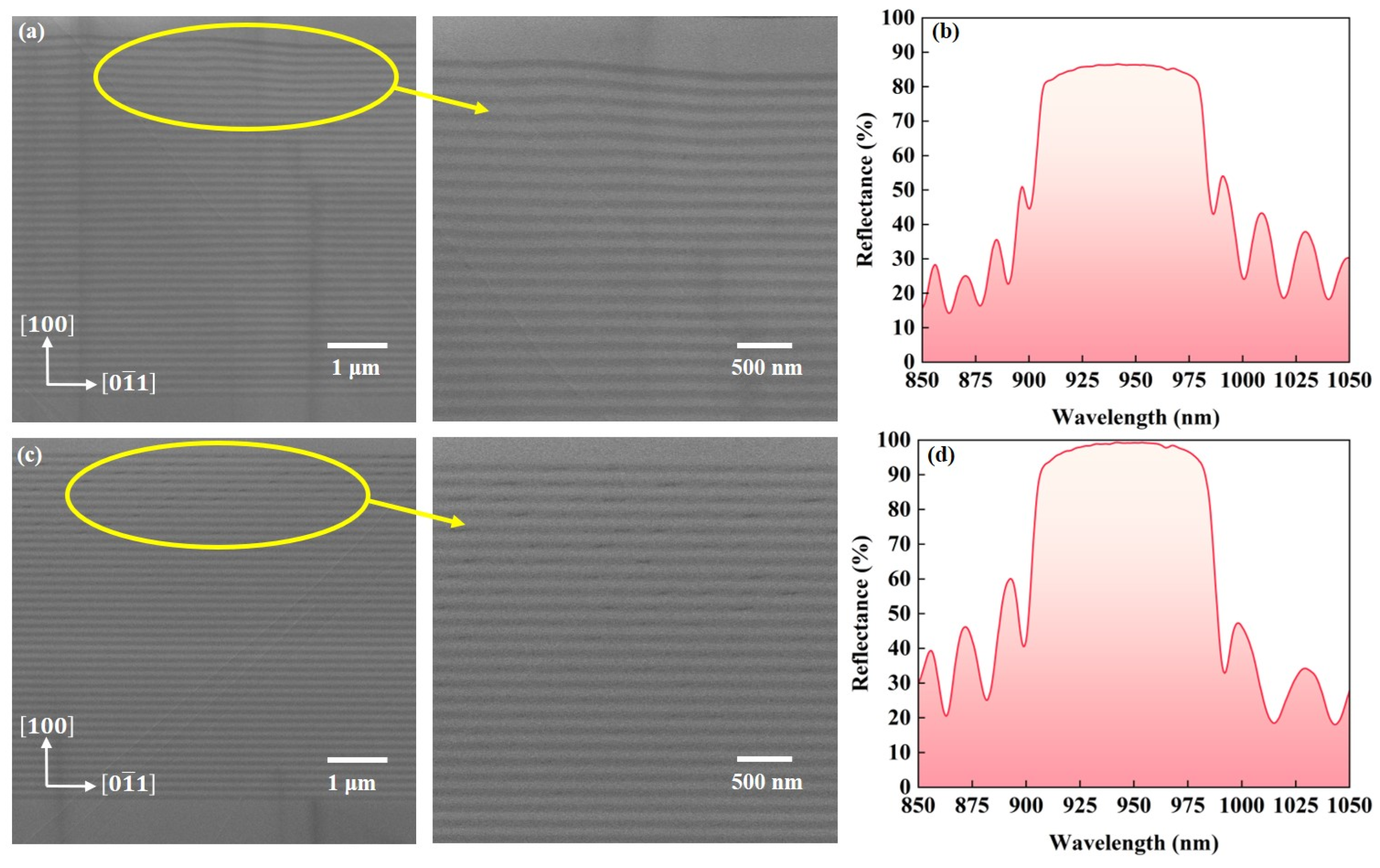
Figure 6 shows the cross-sectional SEM images of the DBR structure grown on top of the photonic crystal and the corresponding reflectance spectra measured at normal incidence under the same conditions. All cross-sectional images were taken above the patterned region, with the p-side facing upward, as indicated in the figure. As shown in Figure 6a, without process optimization, the fabricated DBR exhibited a clearly non-uniform morphology, and the surface flatness was significantly degraded. At this stage, the reflectance spectrum in Figure 6b showed values below 90% in the wavelength range of 940–960 nm. In contrast, as shown in Figure 6c, after DBR optimization, the surface flatness was significantly improved, and reflectance exceeded 99% within the same wavelength in the reflectance spectrum in Figure 6d. This enhancement was primarily attributed to the reduction in interfacial roughness, which effectively suppressed scattering loss [37].
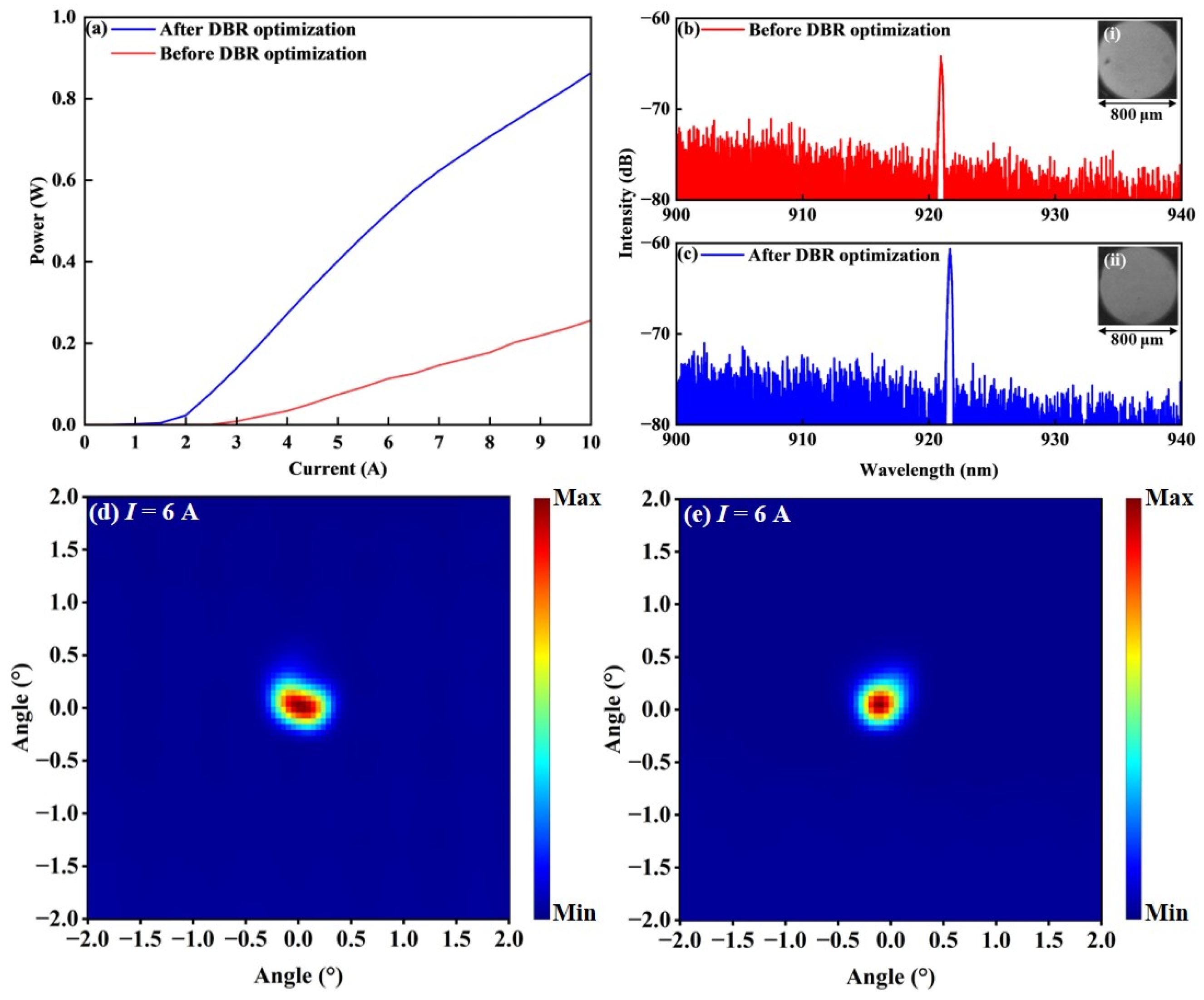
Figure 7 shows the lasing performance of the fabricated PCSEL device with a DBR structure, including its L–I characteristics, emission spectra, and far-field pattern of the device. The emitting region was 800 × 800 μm2. All measurements were carried out under pulsed operation with a pulse width of 10 μs and a repetition rate of 1 kHz. According to the test results, the PCSEL device with an unoptimized DBR exhibited a threshold current (Ith) of 3.01 A and a slope efficiency of 0.04 W/A. Under a pulsed injection current of 10 A, the device delivered an output power of 0.26 W and a beam divergence angle of 1.0°. The relatively low peak power and large divergence angle were attributed to poor DBR interface quality and the deformation of the buried air holes caused by high-temperature growth, which altered their geometric dimensions. In addition, the emission spectra further support this trend: under the same pulsed test condition of 6 A, the device with the optimized DBR exhibited a clearly stronger emission intensity than the device with the unoptimized DBR, as shown in Figure 7b,c. The PL spectrum was measured below the threshold. In contrast, when the PCSEL operates at the working current, the junction temperature is typically higher, and significant self-heating may occur even under pulsed injection. Therefore, the PL emission wavelength can be red-shifted [38]. To obtain an appropriate offset under high-current operation, we intentionally adopted a design in which the resonance wavelength is longer than the PL wavelength. In contrast to the previous design, the PCSEL device fabricated with the optimized DBR structure exhibited significantly improved performance. The threshold current was reduced to 1.87 A, and the slope efficiency increased to 0.13 W/A. Under the same 10 A pulsed operation, the device achieved an output power of 0.86 W and a beam divergence angle of 0.5°. Compared with the non-optimized case, the slope efficiency of the device was improved, and the threshold current was reduced. These enhancements were attributed to the high-quality DBR morphology and the well-defined, asymmetric buried air holes. These results confirm that the optimized DBR structure enabled the realization of a PCSEL device with both high peak power and high beam quality.
We compare the device performance of our approach with the state-of-the-art results detailed in Table 1. The results show that, relative to other reports focused on PCSEL process development, our device exhibits a clear performance advantage, featuring higher output power and a smaller beam divergence angle. This demonstrates that we have achieved significant breakthroughs in the fabrication of the photonic crystal and the DBR, specifically by realizing an asymmetric buried air-hole structure with a large filling factor as well as a high-reflectivity DBR structure, thereby substantially improving the final device performance.
However, when compared with the best performance reported to date, our device still has considerable room for improvement. Current research on PCSELs [14] has achieved continuous-wave (CW) output powers exceeding 50 W, with pure single-mode oscillation and an extremely narrow beam divergence angle of 0.05°, corresponding to a brightness of 1 GW cm−2 sr−1, comparable to the brightness of existing large-scale lasers. Although significant progress has been made in the device in this study, there are still several factors limiting further performance enhancement, such as residual internal optical losses affecting the device’s efficiency, the maximum emitting area required to maintain single-mode operation affecting the output power, and thermal management limitations. To address these issues, we will pursue several improvement pathways in the future to achieve higher-performance PCSEL devices. These include optimizing lithography and etching processes to reduce sidewall roughness and thus lower scattering loss; customizing the photonic-crystal unit cell to expand the single-mode operating area, such as using a double-lattice unit cell design to control the optical coupling within the photonic crystal and achieve stable single-mode oscillation over a larger area; and optimizing packaging and thermal management schemes to enable more efficient heat extraction, thereby improving system stability and output performance. These potential improvements, combined with further optimization of the DBR structure, could lead to enhanced PCSEL device performance.

4. Conclusions

In this study, we introduced a p-type DBR structure consisting of forty pairs of Al0.06GaAs/Al0.9GaAs materials into PCSELs using MOCVD. Both PCSEL epitaxial wafers with and without a DBR structure were fabricated. For the structure without a DBR, we obtained a high-quality epitaxial wafer featuring triangular buried air holes. However, after growing the DBR structure above the buried air holes, the wafer exhibited a significant increase in surface defect density and clear signs of hole deformation, which were related to the mobility of adatoms during high-temperature DBR growth. By selecting appropriate epitaxial conditions for DBR growth, we have effectively controlled adatom diffusion on the wafer surface and inside the air holes. As a result, we achieved a patterned surface with an RMS roughness of only 0.672 nm and obtained uniformly shaped air holes with a filling factor of approximately 18.8% and a depth of about 270 nm. This demonstrates that high-quality DBR structures can be achieved while preserving the morphology of the buried air holes. In addition, we compared the surface morphology of the photonic crystal and non-photonic crystal regions. The non-photonic crystal region showed a lower RMS roughness of 0.525 nm, which is attributed to the propagation of surface roughness from the photonic crystal layer into the DBR. Finally, we successfully fabricated a PCSEL device with a p-type DBR structure. The device exhibited a beam divergence angle of approximately 0.5° and, under a 10 A injection current, delivered a peak power of about 0.86 W. This work presents an effective approach for fabricating DBR-integrated PCSELs using MOCVD and contributes to advancing PCSEL technology toward higher optical output performance.

Author Contributions

Y.Z.: Conceptualization (equal); Data curation (lead); Formal analysis (lead); Investigation (lead); Methodology (lead); Validation (lead); Visualization (lead); Writing—original draft (equal); Writing—review and editing (equal). Y.X.: Project administration (lead); Investigation (supporting); Methodology (supporting); Validation (supporting). Z.Z.: Methodology (supporting); Visualization (supporting). C.L.: Software (supporting); Resources (supporting). C.Z.: Methodology (supporting); Visualization (supporting). L.L. (Longji Li): Visualization (supporting). Y.Y.: Visualization (supporting); Investigation (supporting). M.S.: Resources (supporting); Supervision (supporting). W.Z.: Resources (supporting); Supervision (supporting). L.L. (Liujing Li): Resources (supporting). S.L.: Project administration (supporting). G.D.: Resources (supporting). S.Z.: Resources (supporting). J.W.: Conceptualization (lead); Funding acquisition (lead); Investigation (lead); Supervision (lead); Writing—original draft (equal); Writing—review and editing (equal). All authors have read and agreed to the published version of the manuscript.

Funding

This work was supported by the Jiangsu Province Science and Technology Achievement Transformation Special Fund (BA2023053).

Institutional Review Board Statement

Not applicable.

Informed Consent Statement

Not applicable.

Data Availability Statement

Data related to the results presented in this paper are not publicly available at this time but may be obtained from the authors upon reasonable request.

Acknowledgments

The authors thank Suzhou Everbright Photonics Co., Ltd., for providing technical support and the epitaxy team for MOCVD maintenance.

Conflicts of Interest

Authors Yan Zhang, Yao Xiao, Chen Luo, Chongxi Zhong, Longji Li, Mu Song, Wu Zhao, Liujing Li, Shunfeng Li and Jun Wang were employed by the company Suzhou Everbright Photonics Co., Ltd. The remaining authors declare that the research was conducted in the absence of any commercial or financial relationships that could be construed as a potential conflict of interest.

Abbreviations

The following abbreviations are used in this manuscript:
PCSELsPhotonic-crystal surface-emitting lasers
PCPhotonic crystal
DBRDistributed Bragg reflector
MOCVDMetal–organic chemical vapor deposition

References

  1. Balage, P.; Lopez, J.; Bonamis, G.; Hönninger, C.; Manek-Hönninger, I. Crack-free high-aspect ratio holes in glasses by top–down percussion drilling with infrared femtosecond laser GHz-bursts. Int. J. Extreme Manuf. 2022, 5, 015002. [Google Scholar] [CrossRef] [Scilit]
  2. Zhan, Q.; He, S.; Qian, J.; Cheng, H.; Cai, F. Optimization of optical excitation of upconversion nanoparticles for rapid microscopy and deeper tissue imaging with higher quantum yield. Theranostics 2013, 3, 306–316. [Google Scholar] [CrossRef] [Scilit]
  3. Zhang, C.; Li, H.; Liang, D. Antireflective vertical-cavity surface-emitting laser for LiDAR. Nat. Commun. 2024, 15, 1105. [Google Scholar] [CrossRef] [Scilit] [PubMed]
  4. Zhang, Z.; Xiao, Y.; Zhan, W.; Pan, H.; Li, L.; Liu, H.; Miao, P.; Sun, F.; Cheng, Y.; Zhao, W.; et al. Monolithic 960/1000 nm bicolor semiconductor disk laser delivers a brightness of over 300 MW/cm2sr. ACS Photonics 2025, 12, 2810–2818. [Google Scholar] [CrossRef] [Scilit]
  5. Liang, D.; Zhang, C.; Zhang, P.; Liu, S.; Li, H.; Niu, S.; Rao, R.Z.; Zhao, L.; Chen, X.; Li, H.; et al. Evolution of laser technology for automotive LiDAR, an industrial viewpoint. Nat. Commun. 2024, 15, 7660. [Google Scholar] [CrossRef] [Scilit]
  6. Xiao, Y.; Wang, J.; Liu, H.; Miao, P.; Gou, Y.; Zhang, Z.; Deng, G.; Zhou, S. Multi-junction cascaded vertical-cavity surface-emitting laser with a high power conversion efficiency of 74. Light Sci. Appl. 2024, 13, 60. [Google Scholar] [CrossRef] [Scilit]
  7. Bimberg, D.; Koyama, F.; Iga, K. Highly-efficient VCSEL breaking the limit. Light Sci. Appl. 2024, 13, 123. [Google Scholar] [CrossRef] [Scilit]
  8. Wang, J.; Smith, B.; Xie, X.; Wang, X.; Burnham, G.T. High-efficiency diode lasers at high output power. Appl. Phys. Lett. 1999, 74, 1525–1527. [Google Scholar] [CrossRef] [Scilit]
  9. Chang-Hasnain, C.J.; Orenstein, M.; Von Lehmen, A.; Florez, L.T.; Harbison, J.P.; Stoffel, N.G. Transverse mode characteristics of vertical cavity surface-emitting lasers. Appl. Phys. Lett. 1990, 57, 218–220. [Google Scholar] [CrossRef] [Scilit]
  10. Crump, P.; Böldicke, S.; Schultz, C.; Ekhteraei, H.; Wenzel, H.; Erbert, G. Experimental and theoretical analysis of the dominant lateral waveguiding mechanism in 975 nm high power broad area diode lasers. Semicond. Sci. Technol. 2012, 27, 045001. [Google Scholar] [CrossRef] [Scilit]
  11. Hirose, K.; Liang, Y.; Kurosaka, Y.; Watanabe, A.; Sugiyama, T.; Noda, S. Watt-class high-power, high-beam-quality photonic-crystal lasers. Nat. Photonics 2014, 8, 406–411. [Google Scholar] [CrossRef] [Scilit]
  12. Imada, M.; Noda, S.; Chutinan, A.; Tokuda, T.; Murata, M.; Sasaki, G. Coherent two-dimensional lasing action in surface-emitting laser with triangular-lattice photonic crystal structure. Appl. Phys. Lett. 1999, 75, 316–318. [Google Scholar] [CrossRef] [Scilit]
  13. Yoshida, M.; De Zoysa, M.; Ishizaki, K.; Tanaka, Y.; Kawasaki, M.; Hatsuda, R.; Song, B.; Gelleta, J.; Noda, S. Double-lattice photonic-crystal resonators enabling high-brightness semiconductor lasers with symmetric narrow-divergence beams. Nat. Mater. 2019, 18, 121–128. [Google Scholar] [CrossRef] [Scilit]
  14. Yoshida, M.; Katsuno, S.; Inoue, T.; Gelleta, J.; Izumi, K.; De Zoysa, M.; Ishizaki, K.; Noda, S. High-brightness scalable continuous-wave single-mode photonic-crystal laser. Nature 2023, 618, 727–732. [Google Scholar] [CrossRef] [Scilit] [PubMed]
  15. Persson, L. Simulation and Characterization of Thermal and Optical Effects in Surface-Emitting Lasers. Doctoral Dissertation, Chalmers Tekniska Hogskola, Gothenburg, Sweden, 2025. [Google Scholar]
  16. Morita, R.; Inoue, T.; Yoshida, M.; Enoki, K.; De Zoysa, M.; Ishizaki, K.; Noda, S. Demonstration of high-power photonic-crystal surface-emitting lasers with 1-kHz-class intrinsic linewidths. Optica 2024, 11, 333–339. [Google Scholar] [CrossRef] [Scilit]
  17. Huang, H.; Yang, C.; Li, H.; Zhang, Z. Unveiling the potential of photonic crystal surface emitting lasers: A concise review. Semicond. Sci. Tech. 2025, 40, 043001. [Google Scholar] [CrossRef] [Scilit]
  18. Ishizaki, K.; Sakata, R.; Iwata, K.; Inoue, T.; De Zoysa, M.; Imamura, A.; Yoshida, M.; Hatsuda, R.; Gelleta, J.; Noda, S. Enhancement of slope efficiency of a dually modulated photonic-crystal surface-emitting laser over a wide range of emission angles by introducing a backside reflector. J. Opt. Soc. Am. B 2023, 40, 326–333. [Google Scholar] [CrossRef] [Scilit]
  19. Chen, Y.; Zhang, Z.; Miao, G.; Jiang, H.; Li, Z.; Song, H. AlGaN-based UV-C distributed Bragg reflector with a λ-cavity designed for an external cavity structure electron-beam-pumped VCSEL. J. Alloys Compd. 2020, 820, 153415. [Google Scholar] [CrossRef] [Scilit]
  20. Yoshida, M.; De Zoysa, M.; Ishizaki, K.; Kunishi, W.; Inoue, T.; Izumi, K.; Hatsuda, R.; Noda, S. Photonic-crystal lasers with high-quality narrow-divergence symmetric beams and their application to LiDAR. J. Phys. Photonics 2021, 3, 022006. [Google Scholar] [CrossRef] [Scilit]
  21. Haberland, K.; Zorn, M.; Klein, A.; Bhattacharya, A.; Weyers, M.; Zettler, J.T.; Richter, W. In-situ determination of interface roughness in MOVPE-grown visible VCSELs by reflectance spectroscopy. J. Cryst. Growth 2003, 248, 194–200. [Google Scholar] [CrossRef] [Scilit]
  22. Liu, W.; Ji, X.; Dai, J.; Zhang, J.; Jiao, H.; Cheng, X.; Wang, Z. Study of the free carrier characteristics and surface morphology of AlGaAs/GaAs thin films deposited using MOCVD. Opt. Mater. Express 2024, 14, 629–636. [Google Scholar] [CrossRef] [Scilit]
  23. Tatebayashi, J.; Kako, S.; Ho, J.; Ota, Y.; Iwamoto, S.; Arakawa, Y. Growth of InGaAs/GaAs nanowire-quantum dots on AlGaAs/GaAs distributed Bragg reflectors for laser applications. J. Cryst. Growth 2017, 468, 144–148. [Google Scholar] [CrossRef] [Scilit]
  24. Leonard, J.; Cohen, D.; Yonkee, B.; Farrell, R.; DenBaars, S.; Speck, J.; Nakamura, S. Smooth e-beam-deposited tin-doped indium oxide for III-nitride vertical-cavity surface-emitting laser intracavity contacts. J. Appl. Phys. 2015, 118, 145304. [Google Scholar] [CrossRef] [Scilit]
  25. Yoshida, M.; Kawasaki, M.; De Zoysa, M.; Ishizaki, K.; Hatsuda, R.; Noda, S. Fabrication of photonic crystal structures by tertiary-butyl arsine-based metal–organic vapor-phase epitaxy for photonic crystal lasers. Appl. Phys. Express 2016, 9, 062702. [Google Scholar] [CrossRef] [Scilit]
  26. McKenzie, A.F.; Kyaw, A.M.; Gerrard, N.D.; MacLaren, D.A.; Hogg, R.A. Kinetic influences on void formation in epitaxially regrown GaAs-based PCSELs. J. Cryst. Growth 2023, 602, 126969. [Google Scholar] [CrossRef] [Scilit]
  27. Reilly, K.J.; Kalapala, A.; Yeom, S.; Addamane, S.J.; Renteria, E.; Zhou, W.; Balakrishnan, G. Epitaxial regrowth and hole shape engineering for photonic crystal surface emitting lasers (PCSELs). J. Cryst. Growth 2020, 535, 125531. [Google Scholar] [CrossRef] [Scilit]
  28. Kawaguchi, M.; Miyamoto, T.; Minobe, S.; Koyama, F.; Iga, K. Growth Temperature Dependence of Annealing Effect for GaInNAs/GaAs Quantum Wells Grown by Metalorganic Chemical Vapor Deposition. In Conference Proceedings, 14th Indium Phosphide and Related Materials Conference (Cat. No. 02CH37307); IEEE: New York, NY, USA, 2002; pp. 237–240. [Google Scholar]
  29. Chen, L.-R.; Hong, K.-B.; Huang, K.-C.; Liu, C.-L.; Lin, W.; Lu, T.-C. Study of an epitaxial regrowth process by MOCVD for photonic-crystal surface-emitting lasers. Cryst. Growth Des. 2021, 21, 3521–3527. [Google Scholar] [CrossRef] [Scilit]
  30. Pelucchi, E.; Moroni, S.T.; Dimastrodonato, V.; Vvedensky, D.D. Self-ordered nanostructures on patterned substrates: Experiment and theory of metalorganic vapor-phase epitaxy of V-groove quantum wires and pyramidal quantum dots. J. Mater. Sci. Mater. Electron. 2018, 29, 952–967. [Google Scholar] [CrossRef] [Scilit]
  31. McKenzie, A.F.; King, B.C.; Rae, K.J.; Thoms, S.; Gerrard, N.D.; Orchard, J.; Nishi, K.; Takemasa, K.; Sugawara, M.; Taylor, R.J. Void engineering in epitaxially regrown GaAs-based photonic crystal surface emitting lasers by grating profile design. Appl. Phys. Lett. 2021, 118, 021109. [Google Scholar] [CrossRef] [Scilit]
  32. Wang, Q.; Ma, X.; Wang, H.; Wang, J.; Wang, D. Study on the influence of variable temperature growth on the properties of highly strained InGaAs/GaAs MQWs grown by MOCVD. J. Alloys Compd. 2023, 937, 168075. [Google Scholar] [CrossRef] [Scilit]
  33. Yuan, X.; Pan, D.; Zhou, Y.; Zhang, X.; Peng, K.; Zhao, B.; Deng, M.; He, J.; Tan, H.H.; Jagadish, C. Selective area epitaxy of III–V nanostructure arrays and networks: Growth, applications, and future directions. Appl. Phys. Rev. 2021, 8, 021302. [Google Scholar] [CrossRef] [Scilit]
  34. Shterengas, L.; Liu, R.; Kipshidze, G.; Stein, A.; Lee, W.J.; Hosoda, T.; Zakharov, D.N.; Kisslinger, K.; Belenky, G. Electrically pumped epitaxially regrown GaSb-based type-I quantum-well surface-emitting lasers with buried high-index-contrast photonic crystal layer. Phys. Status Solidi (RRL) Rapid Res. Lett. 2022, 16, 2100425. [Google Scholar] [CrossRef] [Scilit]
  35. Peng, C.; Liang, Y.; Sakai, K.; Iwahashi, S.; Noda, S. Coupled-wave analysis for photonic-crystal surface-emitting lasers on air holes with arbitrary sidewalls. Opt. Express 2011, 19, 24672–24686. [Google Scholar] [CrossRef] [Scilit]
  36. Reuterskiöld Hedlund, C.; Martins De Pina, J.; Kalapala, A.; Liu, Z.; Zhou, W.; Hammar, M. Buried InP/airhole photonic-crystal surface-emitting lasers. Phys. Status Solidi A 2021, 218, 2000416. [Google Scholar] [CrossRef] [Scilit]
  37. Bhattacharya, A.; Zorn, M.; Oster, A.; Nasarek, M.; Wenzel, H.; Sebastian, J.; Weyers, M.; Tränkle, G. Optimization of MOVPE growth for 650 nm-emitting VCSELs. J. Cryst. Growth 2000, 221, 663–667. [Google Scholar] [CrossRef] [Scilit]
  38. Taylor, R.J.; Li, G.; Ivanov, P.; Childs, D.T.; Roberts, T.S.; Stevens, B.J.; Harrison, B.; Sarma, J.; Babazadeh, N.; Terrnent, G. Mode control in photonic crystal surface emitting lasers through external reflection. IEEE J. Sel. Top. Quantum Electron. 2017, 23, 4900208. [Google Scholar] [CrossRef] [Scilit]
  39. Hsu, W.-C.; Miao, W.-C.; Hong, Y.-H.; Kuo, H.-C.; Huang, Y.-W. Monolithically Integrated Metasurface on a PCSEL for Depth Perception. Nano Lett. 2025, 25, 11382–11390. [Google Scholar] [CrossRef] [Scilit] [PubMed]
  40. Chang, C.-J.; Chen, L.-R.; Wu, Y.-J.; Tseng, C.-C.; Hong, K.-B.; Kuo, H.-C.; Lu, T.-C. High power short wavelength infrared photonic crystal surface emitting lasers. J. Light. Technol. 2024, 42, 5262–5268. [Google Scholar] [CrossRef] [Scilit]
  41. Raftery, E.; Lee, D.; Thompson, B.; Chow, K.; Lee, M.L.; Choquette, K.D. Photopumped Buried Dielectric Photonic-Crystal Surface-Emitting Lasers at 1.5 μm. In Proceedings of the 2025 Conference on Lasers and Electro-Optics (CLEO), Long Beach, CA, USA, 4–9 May 2025; IEEE: New York, NY, USA, 2025; pp. 1–2. [Google Scholar]
  42. Bian, Z.; Zhao, X.; Liu, J.; Kim, D.; McKenzie, A.F.; Thoms, S.; Reynolds, P.; Gerrard, N.D.; Kyaw, A.S.; Grant, J. Resonator embedded photonic crystal surface emitting lasers. npj Nanophotonics 2024, 1, 13. [Google Scholar] [CrossRef] [Scilit]
  43. Gautam, C.; Pan, M.; Chen, Y.; Rotter, T.; Balakrishnan, G.; Zhou, W. Laterally coupled photonic crystal surface emitting laser arrays. J. Appl. Phys. 2024, 135, 193108. [Google Scholar] [CrossRef] [Scilit]
Figure 1. Schematic illustration of the regrowth process: (a) initial epitaxial structure on the substrate wafer; (b) formation of triangular air holes in the p-type photonic crystal layer; (c) regrowth of the p-type Al0.42GaAs cladding layer; (d) regrowth of the p-type DBR layers; (e) regrowth of the p-type GaAs contact layer; (f) schematic of the flip-chip PCSEL device.
Photonics 13 00262 g001
Figure 2. (a) Normalized PL spectrum of the MQW in the base epitaxial wafer; (b) X-ray diffraction pattern obtained from HRXRD ω–2θ scan of the base epitaxial wafer; (c) top-view SEM image of the photonic crystal structure processed by electron beam lithography and dry etching; (d) cross-sectional SEM image of the photonic crystal structure.
Photonics 13 00262 g002
Figure 3. (a) Cross-sectional SEM image of the air-hole region along the [ 0 1 ¯ 1 ] direction after regrowth; (b) AFM image of the patterned surface region, with a scan area of 20 μm × 20 μm; (c) optical microscope image of the epitaxial regrowth surface, showing both patterned and unpatterned regions; (d) AFM image of the unpatterned surface region, with a scan area of 20 μm × 20 μm. The measurements in (b–d) were performed on the surface of the p-type GaAs contact layer.
Photonics 13 00262 g003
Figure 4. (a) Cross-sectional SEM image of triangular buried air holes after incorporation of the p-type DBR; (b) AFM image of the patterned surface region, with a scan area of 20 μm × 20 μm; (c) optical microscope image of the epitaxial regrowth surface; (d) AFM image of the unpatterned surface region, with a scan area of 20 μm × 20 μm. The measurements in (b–d) were performed on the surface of the p-type GaAs contact layer.
Photonics 13 00262 g004
Figure 5. (a) Cross-sectional SEM image of the air-hole region along the [ 0 1 ¯ 1 ] direction after DBR optimization; (b) AFM image of the patterned surface region, with a scan area of 20 μm × 20 μm; (c) optical microscope image of the epitaxial regrowth surface; (d) AFM image of the unpatterned surface region, with a scan area of 20 μm × 20 μm. The measurements in (b–d) were performed on the surface of the p-type GaAs contact layer.
Photonics 13 00262 g005
Figure 6. (a) Cross-sectional SEM image of the DBR structure before optimization, taken above the patterned region with the p-side facing upward; (b) reflectance spectrum of the DBR structure before optimization; (c) cross-sectional SEM image of the DBR structure after optimization, taken above the patterned region with the p-side facing upward; (d) reflectance spectrum of the DBR structure after optimization. The reflectance spectra in (b,d) were measured on the DBR surface.
Photonics 13 00262 g006
Figure 7. Laser performance of the device: (a) L–I characteristics; (b,c) emission spectra at an injection current of 6 A. Illustrations i and ii show the near-field mode. Radiation patterns of the device: (d) far-field pattern of the device before DBR optimization; (e) far-field pattern of the device after DBR optimization.
Photonics 13 00262 g007
Table 1. Comparison of our device with state-of-the-art results.
Wavelength (nm)Pulse Width (μs)Output Power (W)Slope Efficiency (W/A)Beam Divergence AngleDimension of Device (μm2)Year
ref [14]940CW500.72~0.05°3000 × 30002023
ref [39]94013.10.14~1°500 × 5002025
ref [40]158010.20.15~1°200 × 2002024
ref [41]15000.3--~2°200 × 2002025
ref [42]130050.030.04~3°200 × 2002024
ref [43]104010.28--100 × 1002024
our device940100.860.13~0.5°800 × 8002025
Disclaimer/Publisher’s Note: The statements, opinions and data contained in all publications are solely those of the individual author(s) and contributor(s) and not of MDPI and/or the editor(s). MDPI and/or the editor(s) disclaim responsibility for any injury to people or property resulting from any ideas, methods, instructions or products referred to in the content.