1. Introduction
Frequency-modulated continuous-wave (FMCW) LIDAR has garnered substantial interest due to its efficient direct velocity measurements and excellent anti-interference characteristics. These applications stand to benefit significantly from the development of mid-infrared lasers with precise frequency control [
1,
2,
3,
4,
5,
6]. The tuning of a single-mode semiconductor laser was accomplished by modulating the cavity refractive index, which, in turn, was performed by generating free carriers in the laser waveguide and active region optically. In the case of optical [
6,
7] control of free carrier concentration, the speed of frequency modulation is limited by carrier recombination time, restricting it to the megahertz range. Electrical frequency modulation of QCL [
8,
9] and diode [
10] lasers was demonstrated in three-terminal devices, where electron concentration inside the cavity is controlled by incorporating a high-electron-mobility transistor into the laser structure. Changes in electron density in the transistor channel induce corresponding variations in the cavity index [
9]. It was shown that optical frequency combs [
11,
12,
13] generated by micro-resonator devices can be used for LIDAR development [
14]. A similar approach was used by Liang et al. [
15] and Dhoore et al. [
16]. The authors of [
15] fabricated a device with an n-InP/SiO
2/Si metal-oxide-semiconductor (MOS) structure embedded in the cavity. When an external voltage is applied between the n-InP and Si layers, electrons and holes accumulate on opposite sides of the dielectric layer, thereby altering the local refractive index.
In FMCW LIDAR, the reflected light from the target is combined with the local reference in a photodetector, converting the round-trip distance to a beat note. Linearity of the laser frequency sweep is an important requirement for LIDAR applications. If the laser frequency sweep is linear, the beat frequency for a stationary target is time-invariant and can be extracted using a Fourier transform (FT). The most tunable lasers do not have an intrinsically linear relation between the optical frequency and the tuning signal. There are two major approaches to this problem: sampled data post-processing [
17,
18] or laser sweep linearization [
19,
20,
21]. The latter includes the application of pre-distortion algorithms for compensation for the frequency sweep nonlinearity. Using this approach, a nonlinearity of 0.005% was demonstrated on commercial vertical cavity surface-emitting lasers [
21]. While real-time nonlinearity correction methods can be applied to various laser types and allow reaching high linearity [
21,
22], they often need complicated structures for the frequency monitoring and require low-latency control circuits and high-performance hardware. The entire system is expensive to build and consequently limits its applications. Therefore, the development of frequency-modulated single-mode semiconductor lasers with internal linear frequency sweep is a crucial task. The high linearity of frequency modulation was demonstrated by the development of the monolithically integrated dual-wavelength distributed feedback (DFB) laser chip [
23]. The chip consists of a phase section between the two DFB lasers with gratings made with the reconstruction-equivalent chirp technique [
24]. Continuous frequency tuning with the range exceeding 30 GHz and tuning nonlinearity of 1.7% was presented in a recent study employing a piezoelectric transducer to scan the cavity length [
25].
In this paper, we propose a simple-to-fabricate three-terminal device for continuous laser frequency tuning [
26]. The approach decouples frequency control bias from the laser driving voltage. A tuning voltage is applied to the heavily doped layer located between the lower cladding and the laser waveguide. This layer works as an intracavity contact. The voltage induces a space-charge-limited current (SCLC) across the lower cladding. The resulting space charge alters the refractive index of the layer, directly affecting the frequency of the emitted light. The tuning speed of the proposed device is limited by the dynamics of space charge formation and dissipation during voltage modulation. These processes are governed by the creation and diffusion of the electron cloud, as well as by the drift of electrons across the cladding layer. Our estimates for the characteristic timescales of these mechanisms fall in the range of 10
−12 to 10
−11 s. The proposed technique is applicable to any semiconductor laser, with two critical requirements: (1) the free carrier concentration in the lower cladding must be sufficiently low to allow effective SCLC operation, and (2) the laser gain must be high enough to compensate for losses introduced by the intracavity contact. For our calculations, we selected a QCL operating near 10 µm. The calculation shows that the device’s frequency shift reaches the gigahertz range with frequency-tuning nonlinearities of 0.38%.
2. Methods
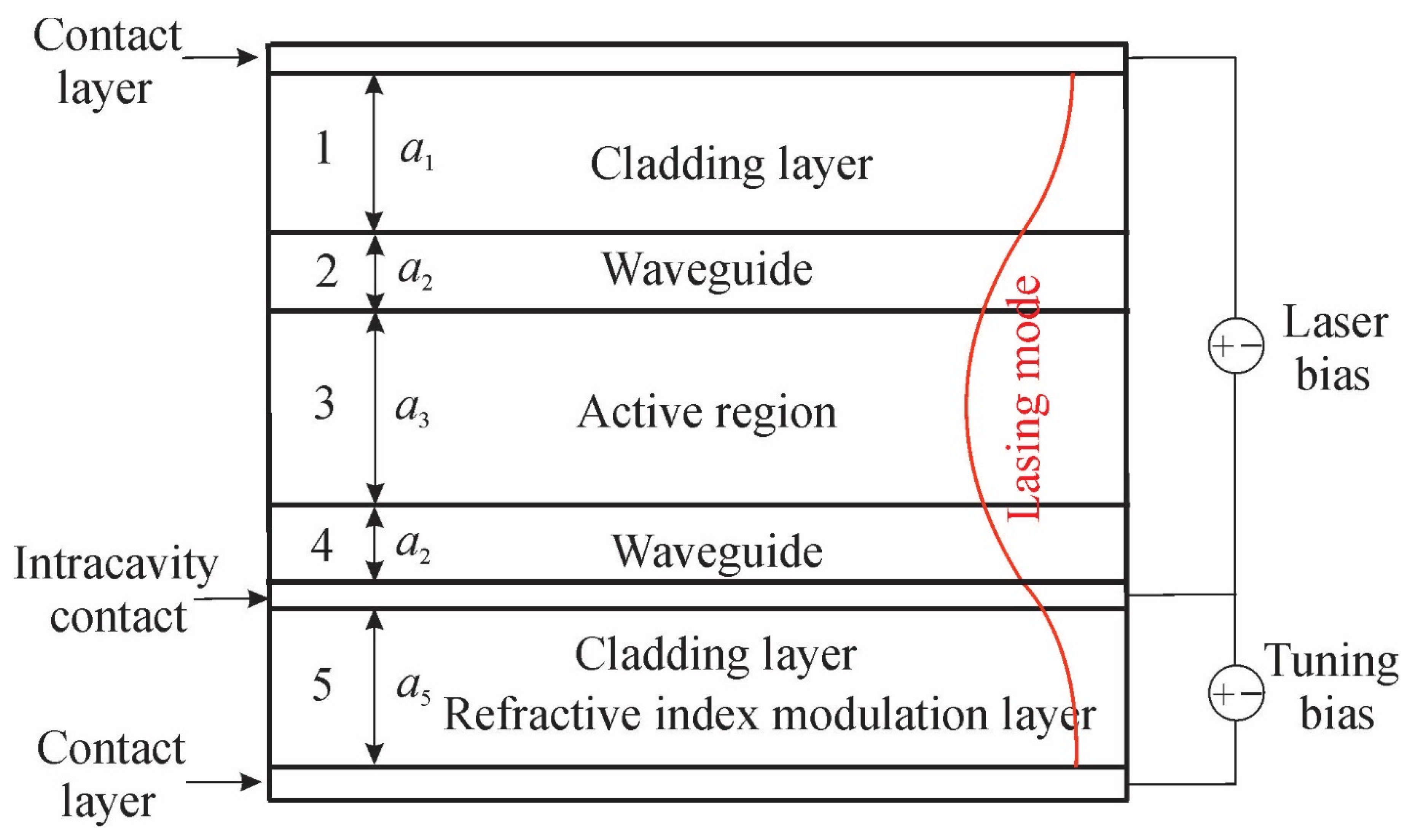
The proposed laser structure is shown in
Figure 1. The active region composed of a Ga
0.47In
0.53As/Al
0.48In
0.52As superlattice is surrounded by two waveguide layers of equal width. The refractive index of the waveguide layer closely matches the average refractive index of the active region. The active region with waveguide layers is embedded between cladding layers composed of Al
0.48In
0.52As, which have a significantly lower refractive index. The contact layer on top of the upper cladding layer, as well as another one between the low wave guide and low cladding layer (referred to as the intracavity contact), are for laser pumping. The low cladding layer is mounted on one more contact layer. This one, together with the intracavity contact, is used for the modulation of free electron concentration within the cladding layer.
The intracavity contact layer is heavily n-doped. Under an electric bias applied between the intracavity contact and the lower contact layer, electrons from the intracavity contact are strongly driven into the lower cladding layer, resulting in an SCLC across the cladding.
The calculation that yields the frequency shift dependence on the applied voltage consists of two parts. The first part computes the light frequency shift resulting from the non-uniform perturbation of the lower cladding layer refractive index. The second part determines the variation in the refractive index in the lower cladding layer as a function of applied bias, creating an SCLC across the layer.
For the cavity mode calculation, it is assumed that the dielectric constant of layers 2, 3, and 4 is the same, and the
and dielectric constants of cladding layers
and
are smaller than
. Without electron injection to cladding layer 5, i.e., at zero bias between the intracavity contact layer and the low contact layer
=
. The widths of the layers,
,
and
, are large compared to the width of the contact layers, and the last one is neglected. If the
z-axis is directed along the wave propagation, and the
x-axis is orthogonal to the layers with origins at the intracavity contact, then the coordinate dependence of the electric field in cavity modes is
In Equations (1a) and (1c), we neglected evanescent waves reflected from outer boundaries of the cladding layers (i.e., proportional to
and
, respectively). Given
, a mode is characterized by two wave vector components,
k in
z direction and
in
x direction. These components are the solution to the equations
where
L is the length of the cavity,
depends on the phases of the mirror reflection coefficients, and
and
are transverse and longitudinal numbers of the mode.
When electric bias is applied between the intracavity contact layer and the low contact layer, electrons are injected in cladding layer 5. The injection changes its dielectric constant, and it becomes
, where
depends on spatial electron distribution in the cladding layer.
x dependence of the dielectric constant leads to a more complicated x-dependence of the electric field in layer 5 than the one seen in Equation (1c). This field is found from the equation
also modifies boundary conditions for
at the interface between layers 4 and 5. (The intracavity contact layer between layers 4 and 5 is very thin and its effect can be neglected.) Dielectric constant variation
is small compared to
and can be considered as a perturbation in both Equation (4) and the boundary conditions. As a result, at
and Equation (3b) is replaced with
where
Wave vector
k is determined by the length of the cavity, and perturbation
η in Equation (6) causes a shift of
, such that
This shift induces perturbation of other wave parameters, given by
and
. As a result, Equation (6) leads to the following dependence of the laser frequency shift
on the perturbation of the refractive index in the low cladding layer
Application of a voltage between the intracavity contact and the bottom contact layer induces a current across the lower cladding layer. However, as long as the cladding layer is undoped, the current is limited by the space charge of electrons that penetrate the cladding layer from the heavily doped intracavity contact. The theory of SCLC was developed by Mott and Gurney [
27] (see also Refs. [
28,
29]). The electron concentration in the cladding layer is
where
is the electron concentration in the intracavity contact layer. Parameter
depends on the current density
j,
( is the static dielectric constant and µ is the electron mobility in the cladding layer).
The
I–
V characteristic of the cladding layer is described by the following equation
Equations (9)–(11) are derived by neglecting the diffusion current. The diffusion current is important at small voltages when the difference in concentration in the doped and undoped regions leads to a potential barrier for electrons at the interface. The width of the barrier is of the order of the Debye screening radius, and its height is of the order of temperature, assuming that the material of both regions is the same. The SCLC takes place at the applied voltage of several tens of volts when the barrier disappears, and diffusion is not important.
The variation in the dielectric constant is connected to free electron concentration according to the relation
where
m is the electron effective mass. Equation (12), along with Equations (9)–(11), defines the refractive index in the low cladding layer as a function of the coordinate and the applied voltage.
We made numerical estimates for the waveguide with the width of the layers , , and refractive indexes , . Then, for wavelength 10 µm (, ), Equation (8) gives, for the relative frequency shift, the estimate with .
3. Results
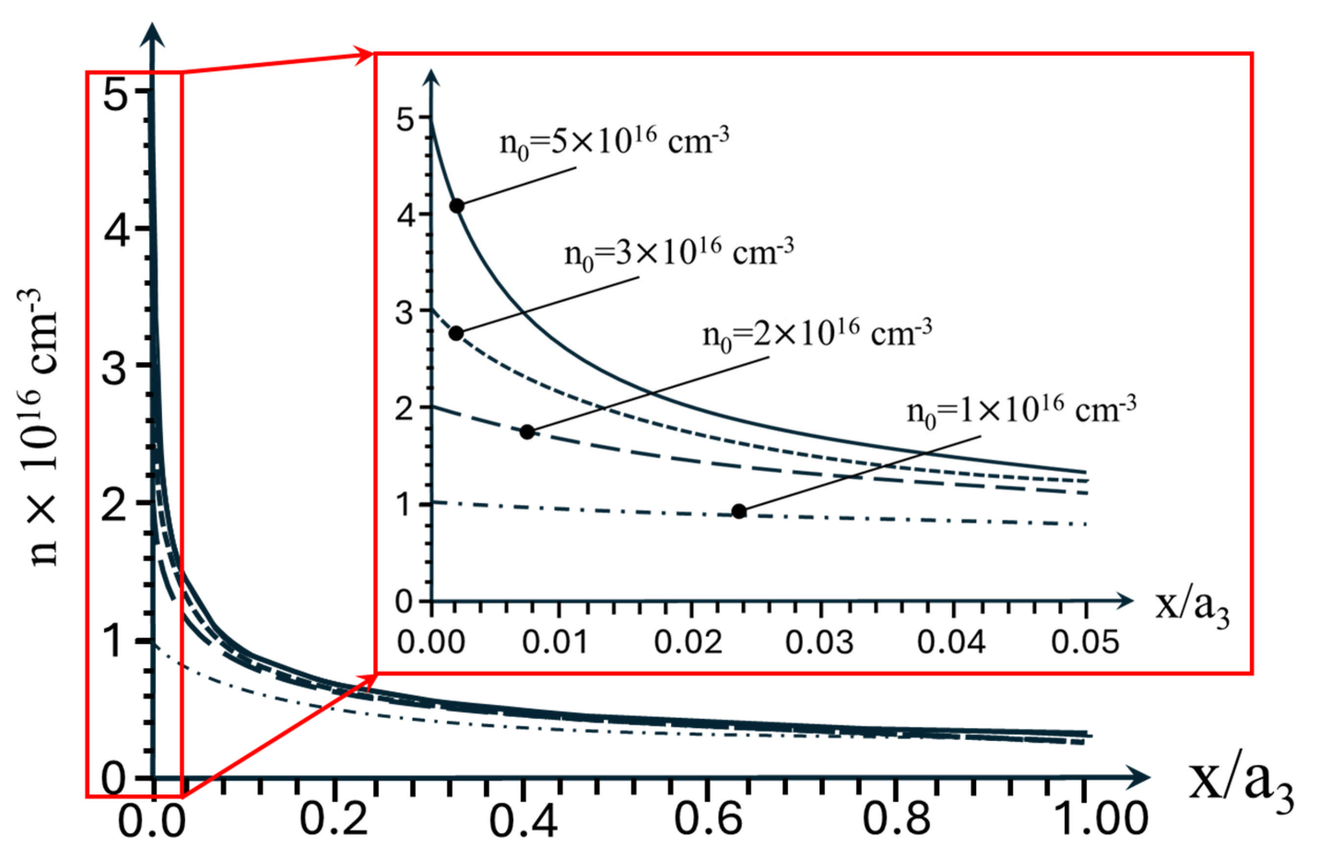
The space charge distribution is shown in
Figure 2. This figure illuminates electron concentration dependence on the distance from the contact in the cladding layer for four different concentrations in the contact at an applied voltage of 20 V. At small distances, the electron concentration near the contact electron concentration in the space charge is close to the contact doping level. The higher the concentration, the faster it falls off, with the distance from the contact in the space charge being close to the concentration in the contact. A higher electron concentration leads to the stronger screening of the contact, which limits the charge extraction and reduces the distance over which the field can pull these electrons. As a result, the higher the concentration, the faster it falls off with the distance. In other words, the higher the concentration, the smaller the distance at which the electric field can pull electrons out from the contact.
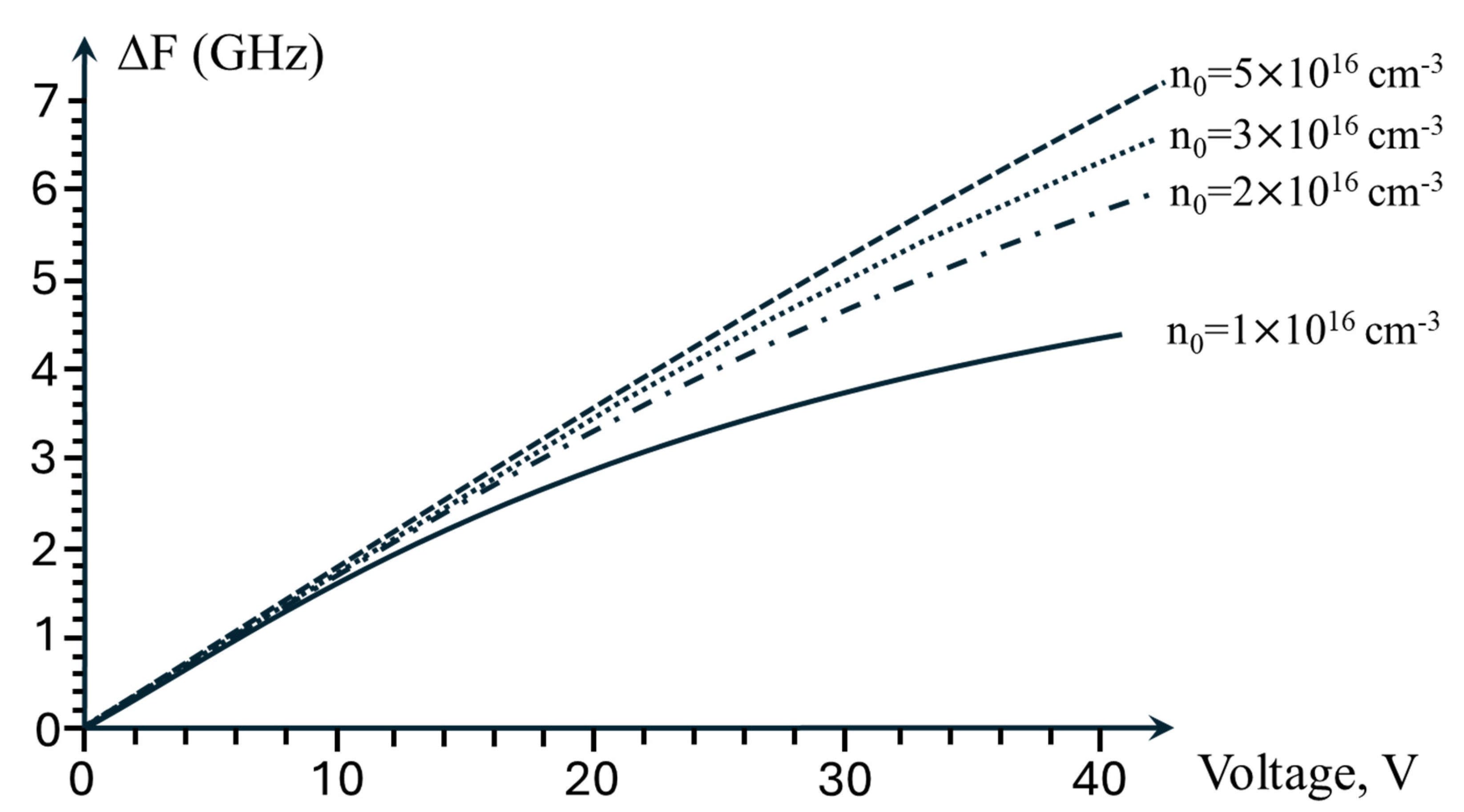
The frequency shift
increases with applied voltage. Voltage dependences of the shift are shown in
Figure 3.
When electrons are extracted from the intracavity contact, the light wave amplitude decreases with distance from the contact. Consequently, the influence of electrons pulled far from the contact is weaker compared to those closer to it. This phenomenon explains the saturation of growth with increasing voltage at low electron concentrations.
Notably, at low voltages, the frequency shift increases linearly with applied voltage. As the electron concentration in the contact increases, the distance over which the voltage can extract electrons decreases, resulting in saturation at higher voltages and an expansion of the linear region. Within the limited accuracy of material constants and structure parameters, we can only give a rough estimate of the nonlinearity of this dependence. For a doping concentration of , the maximal deviation from linearity over the voltage range of 0–20 V is 0.38%, and in the voltage range of 0–40 V, it is 1.2%.
An important consideration is the possible speed of frequency modulation that depends on the time necessary for setting in SCLC by varying the bias voltage. There are two characteristic times relevant to the set in process. One is the Maxwell time, which characterizes the blurring of the electron charge drop,
, where
. The other is the electron drift time across the cladding layer under applied bias,
. Electron mobility of III–V compounds at room temperature is of the order of or larger than
at a doping concentration smaller than
and varies by 2–3 times depending on composition [
30]. Then
is of the order of or smaller than
at
, and
is smaller or of the order of
at
V = 10 V. Both times are so small that the time of setting of the SCLC is likely to be limited by an external circuit.
4. Discussion
In this paper, we propose a simple electrical method for controlling the frequency of semiconductor lasers. Precise frequency tuning is achieved by using the space-charge-limited current (SCLC) technique, which modifies the refractive index of the laser cavity, thus controlling the free carrier concentration in the lower cladding. Since the control of the refractive index is managed by adjusting the electron concentration in a region inside the cavity, but outside the laser’s active region, the modulation of the laser frequency barely affects the device amplitude power. The outlined technique is versatile and can be applied to semiconductor lasers operating at various wavelengths. We calculate the frequency shift (∆f) as a function of the voltage applied to the lower cladding for a quantum cascade laser (QCL) operating near 10 µm wavelength. In our calculations, we neglect the effect of cavity loss on the frequency shift (see Ref. [
8]). Our results indicate that the device’s frequency shift falls within the gigahertz range (see
Figure 3).
It should be noted that carrier injection into the laser cladding generates additional free carrier optical loss, which leads to the modulation of the laser output power. However, this effect is quite small. The additional optical loss is determined by the imaginary part of the change in the effective refractive index of the laser mode. The ratio of the imaginary part of the refractive index to the real part is of the order of , where is the laser frequency; is the electron relaxation time. The ratio between the real and imaginary parts of the frequency shift is the same. In our case, the real part of the frequency shift is , so the The corresponding absorption coefficient is . This is much less than the typical optical loss of a long-wave QCL, which is ~5–8 cm−1. Since the laser output power is proportional to the reciprocal total loss, the expected modulation of the output power due to the additional free-carrier absorption is below 0.1%.
High-resolution frequency-modulated continuous-wave (FMCW) LiDAR relies on a frequency-swept laser [
31]. If the laser frequency sweep is linear, the beat frequency for a stationary target remains time-independent and can be extracted using a Fourier transform. The approach proposed in this paper inherently establishes a linear relationship between the laser frequency shift (∆f) and the voltage (V) applied to the cladding. Data presented in
Figure 3 shows that for a QCL designed according to the presented method, the relative residual nonlinearity of the ∆f dependence can be kept as low as 0.38%. Thus, a three-terminal semiconductor laser with a controllable space-charge-limited current across the lower cladding is easy to fabricate, allowing fast frequency tuning and intrinsically linear laser frequency sweep.


