Abstract
To improve the efficiency and stability of the system, this paper proposes a monolithic integrated optical path design for a cavity optomechanical accelerometer based on a 250 nm top silicon thickness silicon-on-insulator (SOI) wafer instead of readout through U-shape fiber coupling. Finite Element Analysis (FEA) and Finite-Difference Time-Domain (FDTD) methods are employed to systematically investigate the performance of key optical structures, including the resonant modes and bandgap characteristics of photonic crystal (PhC) microcavities, transmission loss of strip waveguides, coupling efficiency of tapered-lensed fiber-to-waveguide end-faces, coupling characteristics between strip waveguides and PhC waveguides, and the coupling mechanism between PhC waveguides and microcavities. Simulation results demonstrate that the designed PhC microcavity achieves a quality factor (Q-factor) of 2.26 × 10⁵ at a 1550 nm wavelength while the optimized strip waveguide exhibits a low loss of merely 0.2 dB over a 5000 μm transmission length. The strip waveguide to PhC waveguide coupling achieves 92% transmittance at the resonant frequency, corresponding to a loss below 0.4 dB. The optimized edge coupling structure exhibits a transmittance of 75.8% (loss < 1.2 dB), with a 30 μm coupling length scheme (60% transmittance, ~2.2 dB loss) ultimately selected based on process feasibility trade-offs. The total optical path system loss (input to output) is 5.4 dB. The paper confirms that the PhC waveguide–microcavity evanescent coupling method can effectively excite the target cavity mode, ensuring optomechanical coupling efficiency for the accelerometer. This research provides theoretical foundations and design guidelines for the fabrication of high-precision monolithic integrated cavity optomechanical accelerometers.
1. Introduction
In recent years, the rapid development of Micro-Opto-Electro-Mechanical System (MOEMSs) technologies has significantly promoted the widespread application of optical microcavity sensors in precision measurement fields. These sensors have become a research hotspot due to their high-sensitivity detection capabilities for physical quantities such as force, displacement, and acceleration, as well as for their excellent immunity to electromagnetic interference [1,2]. Currently, MOEMS accelerometers can be mainly categorized into three types: geometric optical [3,4], wave-optical [5,6,7], and cavity optomechanical [8,9,10]. Among them, cavity optomechanical accelerometers, which utilize optomechanical coupling effects, have attracted increasing attention in recent years owing to their ultra-low noise characteristics and superior on-chip integration potential [11].
Constituting a crucial branch of this field, PhC microcavity optomechanical accelerometers achieve ultra-high-precision measurements by converting acceleration-induced mechanical displacements into variations of optical resonance frequency or light intensity through the coupling between PhC microcavities and mechanical resonators [12]. In the current research, two primary approaches dominate the laser-to-microcavity coupling: U-shaped microfiber direct coupling [13] and integrated silicon waveguide coupling [14]. The former method, while structurally simple, suffers from poor coupling stability that hinders device miniaturization and integrated packaging. The latter approach typically employs either vertical grating couplers or multi-step mode-converting edge couplers [15], yet still faces challenges including low optical integration density and complex fabrication processes, which significantly limit their practical applications.
To address these challenges, this paper proposes an integrated photonic circuit design methodology specifically tailored for cavity optomechanical accelerometers, with particular emphasis on the multiphysics co-optimization of PhC microcavities, silicon strip waveguides, and coupling structures. Our approach comprises four key innovations. First, we employ Plane Wave Expansion (PWE) and FDTD methods to design defect-mode microcavities based on two-dimensional triangular lattices, achieving high-Q resonance at the 1550 nm communication wavelength. Second, tapered transition structures and inverse-taper couplers are systematically optimized to enhance both the mode-field matching between silicon waveguides and PhC waveguides and the fiber-chip edge-coupling efficiency. Third, by applying coupled-mode theory, we realize an evanescent coupling mechanism between the PhC waveguide and microcavity, enabling the efficient excitation of the desired cavity mode. Fourth, based on the FEA and FDTD methods, we quantitatively analyze the loss contributions from each component, ultimately achieving a complete optical circuit model with total insertion loss below 5.4 dB. This paper presents a feasible solution for realizing high-precision, chip-scale cavity optomechanical accelerometers, demonstrating significant application potential in inertial navigation and MOEMS sensing systems.
2. Structural Design of a Strip Waveguide-Integrated Cavity Optomechanical Accelerometer
The proposed integrated silicon strip waveguide accelerometer architecture is illustrated in Figure 1a, comprising five functional modules:

Figure 1.
Schematic of the silicon waveguide-integrated accelerometer structure and working principle. (a) Overall structure of the accelerometer. (b) PhC microcavity structure.
- (1)
- A mechanical sensing module, consisting of a double-ended tuning fork resonator with fixed and movable proof masses forming the vibration system.
- (2)
- An optical sensing module, featuring a PhC microcavity structure formed by two adjacent PhC slabs integrated onto the fixed and movable masses. As shown in Figure 1b, a 100 nm air gap separates the two slabs, with precisely engineered displacements of adjacent air holes (green arrows: 15 nm, blue arrows: 10 nm, and red arrows: 5 nm) creating the optical cavity defect.
- (3)
- An optical transmission module, utilizing silicon strip waveguides as optical channels.
- (4)
- A coupling module, incorporating a three-stage coupling scheme: (i) a lensed fiber-to-waveguide edge coupling at the chip facet, (ii) mode-field matched coupling between strip and PhC waveguides, and (iii) evanescent-wave coupling between the PhC waveguide and microcavity.
The operational principle relies on optomechanical coupling: incident laser light establishes cavity resonance, where radiation pressure drives forced oscillations of the mechanical resonator, thereby encoding vibration information onto the optical signal. The acceleration-modulated optical signal propagates through the waveguide to a photodetector (PD) for optical-to-electrical conversion. Subsequent signal conditioning circuits analyze both the optical signal and its RF components to ultimately determine acceleration with high precision [10]. We employ a Distributed Feedback (DFB) laser with a Gaussian beam as the light source, the stability of which is still a major limiting factor in improving the accelerometer’s performance, particularly in terms of bias instability and measurement accuracy.
The structure was fabricated on an SOI substrate. The employed SOI wafer features the standard tri-layer configuration: a 250-nm-thick top silicon layer, a 3-μm-thick buried oxide (BOX) layer, and a 700-μm-thick silicon handle substrate.
The performance of the PhC microcavity is highly sensitive to micro/nanofabrication tolerances. To enhance the process robustness, parameter optimization was first performed via simulations. The lattice constant a and air-hole radius r were optimized to achieve a sufficiently broad photonic bandgap, aiming to fully encompass the target operational frequency band (187.3–199.8 THz, corresponding to the wavelength range of 1500–1600 nm).
During the fabrication of the PhC microcavity structure using electron-beam lithography (EBL), alignment errors and anisotropic etching effects introduce variations (±10 nm) in the width of the line-defect. To mitigate the impact of these fabrication tolerances, a hierarchical parameter scanning strategy was implemented: for each lattice constant value (a = 480–530 nm), a 6×6 parameter matrix was constructed. Along the vertical axis, the normalized air-hole radius (r/a) was varied from 0.284 to 0.382. Along the horizontal axis, the defect waveguide width was scanned. This approach enables a systematic dual-parameter scan across multiple lattice constants for robust design optimization.
3. Optical Path Simulation of Strip Waveguide-Integrated Cavity Optomechanical Accelerometer
3.1. Optical Mode and Bandgap Simulation of PhC Microcavity
The cavity optomechanical accelerometer developed in this paper employs a PhC microcavity structure. The microcavity is fabricated on a 250 nm thick silicon-on-insulator (SOI) layer fabricated using Electron-Beam Lithography, featuring a triangular lattice of air holes to form the PhC structure. The structural parameters are rigorously optimized with the following dimensions: lattice constant a = 500 nm, air hole radius r = 187.5 nm, and slot width w = 100 nm. The precise control of these geometric parameters ensures that the microcavity resonance wavelength falls within the 1550 nm telecommunication band (1500–1600 nm range) while maintaining a complete photonic bandgap over the operational wavelength range.
The FEA of PhC microcavity resonant frequencies and Q-factors was performed with scattering boundary conditions and physics-controlled mesh refinement. Numerical simulations revealed that the fundamental mode of the microcavity resonates at 1549.15 nm with an optical quality factor (Q) of 2.26 × 10⁵ (Figure 2a), The results showed good agreement with experimental measurements and application requirements [16,17,18]. Additionally, the second-order mode characteristics were thoroughly investigated (Figure 2b). The band structure analysis identified TE-like modes within the photonic bandgap spanning 137.87–218.04 THz (Figure 2c), where a red polyline demarcated the light cone boundary of the photonic crystal (PhC) waveguide. These simulation results provide crucial theoretical foundations for subsequent device performance optimization.
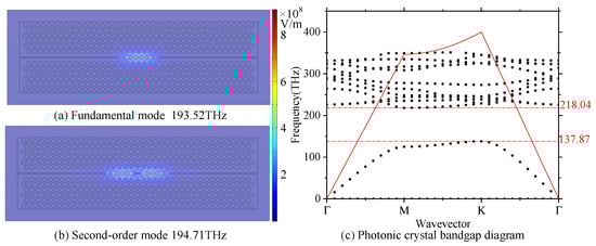
Figure 2.
Optical modes and bandgap characteristics of the PhC microcavity. (a) Fundamental mode. (b) Second-order mode. (c) Band structure along high-symmetry path Γ → M → K → Γ in the first Brillouin zone.
3.2. Silicon Strip Waveguide Transmission Simulation
This paper employs 250 nm thick silicon strip waveguides as the optical transmission medium in the accelerometer chip design. The initial optical characterization of 100 μm long waveguides was conducted via FDTD simulations under the actual refractive index environment (air-clad upper layer and SiO2 substrate). Perfectly matched layer (PML) boundary conditions were applied with a mesh step setting of 0.01 μm and a convergence criterion of 10−5. Figure 3a presents the transmittance characteristics at 1550 nm as a function of waveguide width, demonstrating a monotonic increase in transmission efficiency from 200 nm to 500 nm, with transmittance exceeding 99.9% for widths beyond 470 nm.
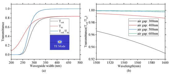
Figure 3.
Simulation results of silicon strip waveguide transmission characteristics. (a) Dependence of transmittance on waveguide width with corresponding mode profiles. (b) Effect of sidewall trench width on optical transmittance.
Modal analysis conducted using FEA revealed that single-mode operation could be maintained within the 260–560 nm width range. Through the comprehensive evaluation of multiple design constraints including single-mode propagation requirements, high transmission efficiency (>99.9%), and structural integrity considerations during the HF-based fabrication of long-range waveguides, an optimal waveguide width of 470 nm was determined. This configuration achieves a TE mode effective refractive index of 2.4381 with 99.92% transmittance, meeting both optical performance specifications and fabrication feasibility.
The investigation of sidewall trench width effects on optical performance (Figure 3b) demonstrated that while a 300 nm trench yields 95% transmittance for 100 μm waveguides at 1550 nm, the cumulative total loss exceeds 10 dB for the full 5000 μm device length, rendering this configuration impractical for application.
Further parameter optimization revealed significant performance improvements with trench widths exceeding 600 nm: short-length (100 μm) transmittance >99.9%, with total propagation loss reduced to 0.2 dB for 5000 μm.
These findings conclusively demonstrate that an increased trench width effectively mitigates long-distance propagation losses, providing critical design guidelines for practical implementation.
3.3. Simulation of Edge Coupling Structure
Edge coupling refers to the transverse optical coupling between tapered-lensed fibers and silicon waveguide facets, for which the symmetric suspended photonic waveguide is the best candidate. However, the intrinsic mechanical modes introduced by the suspended structure may affect the operational performance of the optomechanical accelerometer. Therefore, the asymmetric cladding (air upper layer/SiO2 lower layer) waveguide structure is adopted, which causes modal field distortion and displacement. The direct implementation of the 100 nm edge-width taper [19] yields unacceptable 15 dB coupling loss.
To address this asymmetry, we propose a taper design (Figure 4a) with unique modal characteristics: narrow facets (~0.1 μm) exhibiting SiO2-confined modes (Figure 4b). Through rigorous numerical optimization, we achieved 2–3 μm mode field diameter (MFD) matching with lensed fibers (Figure 4c).
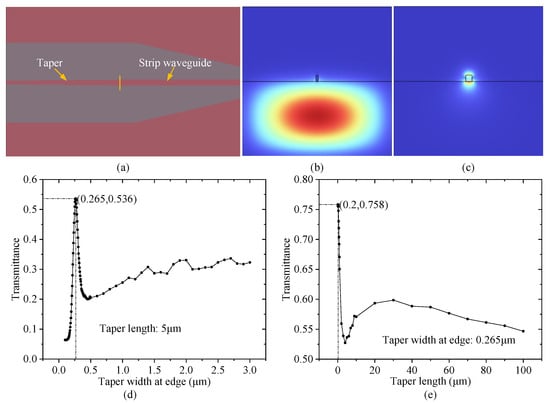
Figure 4.
Edge coupling structure and simulation results. (a) Schematic of the edge coupling structure. (b) Mode field distribution with 0.1 μm waveguide facet width. (c) Mode field distribution with 0.265 μm waveguide facet width. (d) Transmission efficiency versus facet width of the coupling structure. (e) Transmission efficiency versus length of the coupling structure.
Through systematic parameter optimization (Figure 4d,e), we balanced three critical factors: optical performance requirements, fabrication process constraints, and structural reliability considerations. The yielded optimal parameters were as follows: 265 nm facet width and 30 μm length. This length ensures both process robustness (<20 μm tapers suffer polishing damage) and optical performance.
Verified results from 3D FDTD demonstrate 2.2 dB coupling loss at 1550 nm, meeting practical requirements. The design successfully balances high efficiency with manufacturability in asymmetric cladding environments.
3.4. Coupling Simulation of Silicon Strip Waveguides and PhC Waveguides
To achieve efficient mode coupling between the silicon strip waveguide (width = 470 nm) and PhC waveguide (width: 880 nm), this paper designs a tapered coupling structure to address their width mismatch. The waveguide transition structure is optimized using a polynomial taper function with m = 0.2, and a 3D simulation model is established (Figure 5a).
Figure 5.
Coupling simulation between silicon strip waveguide and PhC waveguide. (a) Simulation model. (b) Mode field distribution. (c) Transmission spectrum.
Simulation results demonstrate that the structure exhibits excellent mode conversion characteristics at the operating wavelength of 1550 nm. The electric field distribution (Figure 5b) shows that the optical field can be effectively coupled into the PhC waveguide. Transmission spectrum analysis (Figure 5c) reveals a transmission efficiency of 92% at this wavelength, corresponding to a total insertion loss of only 0.4 dB, which verifies the high coupling efficiency of the designed tapered structure.
3.5. Coupling Simulation of PhC Waveguide and Optical Microcavity
This paper systematically investigates the non-destructive coupling mechanism between PhC waveguides and optical microcavities using the FDTD simulation platform. As shown in Figure 6a, through the selective removal of the third row of air holes above the air slot (while retaining four critical air holes), we successfully establish a waveguide–microcavity coupling system with subwavelength spacing while maintaining the structural integrity of the microcavity (yellow hexagonal region). This design not only preserves the intrinsic geometric characteristics of the microcavity but also achieves efficient optical field coupling.
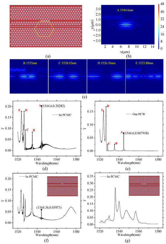
Figure 6.
Coupling simulation showing silicon strip waveguide and PhC waveguide. (a) Simulation model. (b) Fundamental mode. (c) Other resonant modes. (d) Transmission spectrum of PCMC. (e) Transmission spectrum of PCW. (f) Destructive coupling model with third-row modification and corresponding microcavity transmission spectrum. (g) Non-destructive coupling model with second-row modification and corresponding microcavity transmission spectrum.
The simulation results (Figure 6b–e) reveal five characteristic resonance peaks (A–E) in both the microcavity transmission spectrum and the output spectrum from the PhC waveguide end, corresponding to wavelengths of 1544.6 nm, 1535 nm, 1528.02 nm, 1526.56 nm, and 1523.88 nm. Among these, Mode A (Figure 6b) exhibits typical fundamental mode characteristics of the microcavity: the optical field is highly localized within the microcavity, with an electric field intensity enhancement factor exceeding 40. Figure 6c displays four additional resonance modes (labeled B–E), whose field distributions indicate they are undesired microcavity resonance modes. Figure 6d,e show the transmittance curves inside the PCMC and at the output of the right-side PCW, respectively. Notably, the slight discrepancy between the fundamental mode wavelength (1544.6 nm) and the FEA result (1549.15 nm) in Section 3.1 arises from inherent differences between the two methods: FEA excels in mode field analysis whereas FDTD more accurately captures transmission effects. Due to the evanescent coupling mechanism, our analysis focused on the excitation efficiency of the desired modes, and thus, end-to-end transmission (Tout/Tin) was not quantified.
Additionally, to optimize the coupling structure, we compared several coupling schemes (Figure 6f,g): (1) the additional removal of two air holes from the third row compromised the microcavity structure, significantly reducing fundamental mode energy; (2) the removal of the second row air holes maintained microcavity integrity but caused resonance frequency shift, energy reduction, and Q-factor degradation; (3) other approaches (e.g., removing first/fourth row air holes) demonstrated inferior coupling efficiency.
Comprehensive analysis confirms that the structure shown in Figure 6a delivers optimal coupling performance, with its outstanding low-loss and high-directionality characteristics providing crucial technical support for weak-light manipulation in cavity optomechanical systems.
4. Discussion
Manufacturing tolerances have a certain degree of impact on the performance of the optical path. Our team analyzed, in detail, the effects of the lattice constant, air hole radius and tilt angle, and air slot width on the Q-factor and resonant frequency in another article [20]. Hole radius deviation (±Δr) primarily affects the Q-factor and resonant wavelength, showing the most significant sensitivity. Line-edge roughness (LER) strongly influences scattering loss and Q-factor degradation. Lattice constant shift (Δa) moderately impacts the bandgap position and coupling efficiency while etching depth non-uniformity (Δd) exhibits a relatively lower effect on vertical loss and the Q-factor. Based on this parameter sensitivity ranking, we adopted a design targeting low-sensitivity ranges and validated through simulation optimization, confining the air hole radius to be 180 nm ± 10 nm and the lattice constant to be 500 nm ± 10 nm.
For subsequent experimental verification, the system loss and bandgap characteristics will be calibrated using tapered fiber end coupling and tunable laser scanning. Although cavity optomechanical accelerometers exhibit promising sensitivity and dynamic range [10], challenges persist in system integration and practical deployment. These include stability issues in on-chip lasers/photodetectors, the thermal sensitivity of silicon materials, and nonlinear dynamics—evidenced by observed self-induced regenerative oscillations and parametric optomechanical oscillations in silicon integrated cavities [21]. To suppress nonlinear effects on measurement accuracy, the pump power will be maintained in the microwatt regime, with additional thermoelectric cooling (TEC) mitigating thermal drift.
5. Conclusions
This paper has presented an optical design scheme for a monolithically integrated cavity optomechanical accelerometer based on a 250 nm thick top silicon thickness SOI wafer using the FEA and FDTD method to systematically investigate the performance of key optical structures. By optimizing the PhC microcavity, strip waveguide, edge coupling structure, and waveguide–microcavity coupling mechanism, a low-loss and high-efficiency optical system has been achieved. Compared to other cavity optomechanical accelerometers [9,10,14], our design features a higher microcavity Q-factor, improved integration level and coupling stability, and easier fabrication.
The main conclusions are as follows:
- (1)
- PhC Microcavity Design Optimization: The designed microcavity exhibits a quality factor (Q-factor) of 2.26 × 10⁵ at a wavelength of 1550 nm, meeting the requirements for high-sensitivity optomechanical coupling. The PhC bandgap effectively suppresses interference from non-resonant optical modes, ensuring microcavity mode stability.
- (2)
- Low-Loss Waveguide Transmission: The optimized strip waveguide demonstrates a loss of only 0.2 dB over a 5000 μm transmission length, enabling long-distance, low-loss optical signal transmission.
- (3)
- High-Efficiency Coupling Structures:
The coupling between the silicon waveguide and the PhC waveguide achieves a transmission efficiency of 92% (loss < 0.4 dB) at the resonant frequency, indicating excellent mode matching.
The optimized tapered lens fiber-to-waveguide edge coupling yields a transmission efficiency of 75.8% (loss < 1.2 dB). Considering process feasibility, a 30 μm coupling length scheme (transmission efficiency 60%, loss ~2.2 dB) was selected to balance performance and fabrication complexity.
- (4)
- Optical System Performance:
The total loss from the input to the output port is 5.4 dB, confirming the low-loss characteristics of the designed optical path and meeting the detection requirements of high-precision accelerometers.
- (5)
- Waveguide–Microcavity Coupling Mechanism:
The paper has confirmed that the PhC waveguide–microcavity blockade coupling method effectively excites the target microcavity mode, avoids mode competition, and ensures optomechanical coupling efficiency, laying the foundation for high-sensitivity accelerometer detection.
This research provides theoretical foundations and design guidelines for the fabrication of high-precision monolithically integrated cavity optomechanical accelerometers. The proposed optical scheme achieves a favorable balance between process feasibility and performance optimization, offering critical insights for subsequent device fabrication and testing. For practical applications, future work may further explore the impact of process variations on optical performance and experimentally validate the practical performance of the device.
Author Contributions
Conceptualization, C.X. and Y.H., methodology, C.X. and R.Z., software, C.X., validation, Z.L., Y.Z. and C.W., investigation, C.X., writing—original draft preparation, B.F., writing—review and editing, B.F., Y.H., G.W. and P.K., supervision. All authors have read and agreed to the published version of the manuscript.
Funding
This work was supported in part by the National Natural Science Foundation of China (project contract nos. 62371106, U2230206 and 62204264), in part by the National Key R&D Program (project contract no. 2022YFA1405900), in part by the China Postdoctoral Science Foundation (project contract no. 2023M740534), and in part by the Innovation Ability Construction Project for Sichuan Provincial Engineering Research Center of Communication Technology for Intelligent IoT (2303-510109-04-03-318020).
Institutional Review Board Statement
Not applicable.
Informed Consent Statement
Not applicable.
Data Availability Statement
The data will be made available on request.
Conflicts of Interest
The authors declare that the research was conducted in the absence of any commercial or financial relationships that could be construed as potential conflicts of interest.
Abbreviations
| BOX | Buried Oxide |
| DFB | Distributed Feedback |
| EBL | Electron-Beam Lithography |
| FDTD | Finite-Difference Time-Domain |
| FEA | Finite Element Analysis |
| LER | Line-Edge Roughness |
| MOEMS | Micro-Opto-Electro-Mechanical Systems |
| PD | Photodetector |
| PCMC | Photonic Crystal Microcavity |
| PCW | Photonic Crystal Waveguide |
| PhC | Photonic Crystal |
| PWE | Plane Wave Expansion |
| PML | Perfectly Matched Layer |
| SOI | Silicon-On-Insulator |
| TEC | Thermoelectric Cooling |
References
- Aspelmeyer, M.; Aspelmeyer, M.; Kippenberg, T.J.; Marquardt, F. Cavity optomechanics. Rev. Mod. Phys. 2014, 86, 1391–1452. [Google Scholar] [CrossRef]
- Li, M.; Pernice, W.H.P.; Tang, H.X. Broadband all-photonic transduction of nanocantilevers. Nat. Nanotechnol. 2009, 4, 377–382. [Google Scholar] [CrossRef] [PubMed]
- Tang, S.; Liu, H.; Yan, S.; Xu, X.; Wu, W.; Fan, J.; Liu, J.; Hu, C.; Tu, L. A high-sensitivity MEMS gravimeter with a large dynamic range. Microsyst. Nanoeng. 2019, 5, 45. [Google Scholar] [CrossRef] [PubMed]
- Sheikhaleh, A.; Abedi, K.; Jafari, K.; Gholamzadeh, R. Micro-optoelectromechanical systems accelerometer based on intensity modulation using a one-dimensional PhC. Appl. Opt. 2016, 55, 8993–8999. [Google Scholar] [CrossRef] [PubMed]
- Lu, Q.; Bai, J.; Wang, K.; He, S. Design, optimization, and realization of a high-performance MOEMS accelerometer from a double-device-layer SOI wafer. J. Microelectromechan. Syst. 2017, 26, 859–869. [Google Scholar] [CrossRef]
- Nie, Y.; Huang, K.; Yang, J.; Cao, L.; Cheng, L.; Wang, Q.; Tian, H.; Peihua, W.; Heng, L. A proposal to enhance high-frequency optical MEMS accelerometer sensitivity based on a one-dimensional PhC wavelength modulation system. IEEE Sens. J. 2020, 20, 14639–14645. [Google Scholar] [CrossRef]
- Taghavi, M.; Latifi, H.; Parsanasab, G.M.; Abedi, A.; Nikbakht, H.; Poorghadiri, M.H. A dual-axis MOEMS accelerometer. IEEE Sens. J. 2021, 21, 13156–13164. [Google Scholar] [CrossRef]
- Li, Y.L.; Barker, P.F. Characterization and testing of a micro-g whispering gallery mode optomechanical accelerometer. J. Light. Technol. 2018, 36, 3919–3926. [Google Scholar] [CrossRef]
- Krause, A.G.; Winger, M.; Blasius, T.D.; Lin, Q.; Painter, O. A high-resolution microchip optomechanical accelerometer. Nat. Photonics 2012, 6, 768–772. [Google Scholar] [CrossRef]
- Huang, Y.; Flor Flores, J.G.; Li, Y.; Wang, W.; Wang, D.; Goldberg, N.; Zheng, J.; Yu, M.; Lu, M.; Kutzer, M.; et al. A chip-Scale oscillation-Mode optomechanical inertial sensor near the thermodynamical limits. Laser Photonics Rev. 2020, 14, 1800329. [Google Scholar] [CrossRef] [PubMed]
- Safavi-Naeini, A.H.; Gröblacher, S.; Hill, J.T.; Chan, J.; Aspelmeyer, M.; Painter, O. Squeezed light from silicon resonators. Nat. 2013, 500, 185–189. [Google Scholar] [CrossRef]
- Eichenfield, M.; Chan, J.; Camacho, R.M.; Vahala, K.J.; Painter, O. Optomechanical crystals. Nature 2009, 462, 78–82. [Google Scholar] [CrossRef] [PubMed]
- Flor Flores, J.G.; Yerebakan, T.; Wang, W.; Yu, M.; Kwong, D.L.; Matsko, A.; Wong, C.W. Parametrically Driven Inertial Sensing in Chip—Scale Optomechanical Cavities at the Thermodynamical Limits with Extended Dynamic Range. Laser Photonics Rev. 2023, 17, 2200827. [Google Scholar] [CrossRef]
- Liu, H.; She, X.; Shen, H.; Chen, L.; Bi, R.; Chen, K.; Shu, X. Monolithic integrated cavity optomechanical accelerometer based on push-pull photonic crystal zipper cavity. Opt. Eng. 2023, 62, 037107. [Google Scholar] [CrossRef]
- Khilo, A.; Popović, M.A.; Araghchini, M.; Kärtner, F.X. Efficient Planar Fiber-to-Chip Coupler Based on Two-Stage Adiabatic Evolution. Opt. Express 2010, 18, 15790–15806. [Google Scholar] [CrossRef]
- Joannopoulos, J.D.; Johnson, S.G.; Winn, J.N.; Meade, R.D. Photonic Crystals: Molding the Flow of Light, 2nd ed.; Princeton University Press: Princeton, NJ, USA, 2008. [Google Scholar]
- Song, B.-S.; Noda, S.; Asano, T.; Akahane, Y. Ultra-high-Q photonic double-heterostructure nanocavity. Nat. Mater. 2005, 4, 207–210. [Google Scholar] [CrossRef]
- Asano, T.; Noda, S. High-Q photonic nanocavity. In Proceedings of the SPIE 5515, Nanoengineering: Fabrication, Properties, Optics, and Devices, Denver, CO, USA, 8 October 2004. [Google Scholar] [CrossRef]
- Almeida, V.R.; Panepucci, R.R.; Lipson, M. Nanotaper for compact mode conversion. Opt. Lett. 2003, 28, 1302–1304. [Google Scholar] [CrossRef] [PubMed]
- Muhammad, S.; Chen, D.; Xian, C.; Zhou, J.; Lei, Z.; Kuang, P.; Ma, L.; Wen, G.; Fan, B.; Huang, Y. Parameter investigations of waveguide-integrated lithium niobate photonic crystal microcavity. Photonics 2025, 12, 475. [Google Scholar] [CrossRef]
- Wu, J.; Huang, S.-W.; Huang, Y.; Zhou, H.; Yang, J.; Liu, J.-M.; Yu, M.; Lo, G.; Kwong, D.-L.; Duan, S.; et al. Mesoscopic chaos mediated by Drude electron-hole plasma in silicon optomechanical oscillators. Nat. Commun. 2017, 8, 15570. [Google Scholar] [CrossRef] [PubMed]
Disclaimer/Publisher’s Note: The statements, opinions and data contained in all publications are solely those of the individual author(s) and contributor(s) and not of MDPI and/or the editor(s). MDPI and/or the editor(s) disclaim responsibility for any injury to people or property resulting from any ideas, methods, instructions or products referred to in the content. |
© 2025 by the authors. Licensee MDPI, Basel, Switzerland. This article is an open access article distributed under the terms and conditions of the Creative Commons Attribution (CC BY) license (https://creativecommons.org/licenses/by/4.0/).