Abstract
This work presents a novel gas sensor based on a slotted polymer-phaseshift Bragg grating (SP-PSBG) waveguide filled with polyhexamethylene biguanide (PHMB) as the sensing medium. The transmission resonance, characterized by a narrow peak with a full width at half maximum (FWHM) of 1.6 nm within the Bragg grating bandgap, is highly responsive to refractive index changes in PHMB caused by variations in concentration. Numerical simulations demonstrate a sensitivity of 14.4 pm/ppm, outperforming conventional gas sensors based on functional material coatings. This enhanced performance comes from the direct interaction between the PHMB-filled resonant structure and the cladding that contains molecules, eliminating the need for polymer-coated cladding layers. The optimization approach employed in this design focuses on maximizing the optical confinement factor within the PHMB-filled slot, leading to an effective overlap between the guided optical mode and the sensing material.
1. Introduction
Gas sensors are essential devices for detecting toxic and hazardous gases in various environments, including industrial facilities and residential areas [1]. Traditionally, gas detection has relied on techniques such as gas chromatography [2,3]; however, these methods often require bulky equipment and long processing times and may be affected by environmental factors such as air quality and particulate matter [4]. In recent years, there has been a growing interest in compact, sensitive, and rapid-response alternatives. Optical gas sensors, particularly those leveraging photonic technologies, offer several advantages including high sensitivity, fast detection, and easy integration into portable systems [5,6,7,8].
Photonic gas sensors utilize light–matter interaction to determine gas concentrations in the air through different mechanisms, including absorption-based detection and refractive index (RI) sensing. Absorption-based sensors depend on the characteristic absorption spectra of the target gas, where specific wavelengths are absorbed depending on the gas concentration. Light intensity is measurably attenuated because of this absorption, and this attenuation can be correlated to gas concentration [9]. In contrast, RI-based sensors operate by detecting shifts in the resonance wavelength due to changes in the optical properties of the surrounding medium. This happens when the local RI is altered by changes in gas content, which results in detectable shifts in optical resonances [10].
Silicon photonics is a highly promising platform for developing highly sensitive gas sensors due to its compatibility with well-established complementary metal-oxide–semiconductor (CMOS) fabrication processes [11]. This enables the production of compact, scalable, and cost-effective photonic devices suitable for real-time sensing applications. The silicon-on-insulator (SOI) platform, widely used in photonic integrated circuits, offers a high RI contrast, allowing strong optical confinement and low propagation losses [12], which are essential for high-sensitivity sensing.
RI sensors mainly depend on resonator structures, such as micro-ring resonators [13], Bragg gratings [14], guided-mode resonance (GMR) [15], surface plasmon resonance (SPR) [16], and Mach–Zehnder interferometers [17], to track resonance shifts caused by changes in the surrounding RI due to changes in analyte concentration. Unlike solutions and biosensors [18,19], gas detection demands highly sensitive devices capable of detecting minimal RI variations [20], posing a significant challenge in the design of RI-based SOI gas sensors. The sensing performance of integrated photonic platforms is fundamentally determined by the strength of the interaction between the guided optical field and the surrounding analyte. One effective strategy to enhance light–analyte interaction in integrated photonic sensors is the use of strip-slot waveguides, which confine a substantial portion of the optical mode within low-index regions. This configuration can greatly enhance RI sensing performance when combined with resonant structures like micro-ring resonators or Bragg gratings [21,22]. To boost the sensitivity of gas detection, another promising approach used to enhance the sensitivity of RI sensors is the integration of polymer-based materials. Polymer coatings can strongly interact with the target gas, leading to changes in their RI as a function of gas concentration. This effect can be precisely enhanced to track wavelength sensitivity using resonant photonic structures [23,24]. Among such materials, polyhexamethylene biguanide (PHMB) has been extensively studied due to its strong and reversible changes in RI induced by [25]. When deposited on photonic structures, PHMB enhances light–matter interactions due to changes in its refractive index in response to gas concentration, leading to improved detection limits and higher sensitivity. Several PHMB-based sensor technologies have been developed, each offering distinct advantages. Plasmonic-based PHMB sensors, for example, provide high sensitivity due to strong field confinement [26,27,28], while SOI-based PHMB sensors offer easier integration with silicon photonics and improved thermal stability. These characteristics make the integration of PHMB with SOI devices a versatile and effective approach for gas sensing applications [29].
A recent study developed a silicon photonic dual-gas sensor for simultaneous and detection using a micro-ring resonator array as seen in [30]. The sensor utilized a 620 nm PHMB polymer layer for sensing and a palladium (Pd) layer for detection. The PHMB-coated micro-ring achieved a sensitivity of pm/ppm, with a detection limit of 370 ppm, while demonstrating negligible cross-sensitivity to . Conversely, the Pd-functionalized micro-ring exhibited a sensitivity of pm/ppm for but also responded to with a cross-sensitivity of pm/ppm. In another study [31], a 240 nm PHMB polymer layer is used in a silicon photonic sensor based on a micro-ring resonator to detect in the atmosphere. The sensor can function at room temperature without relying on humidity, thanks to the PHMB coating, which makes it possible to detect changes in RI in response to concentration. The device achieves a high sensitivity of RIU/ppm with a detection limit of 20 ppm, offering a compact and low-cost solution for accurate greenhouse gas monitoring. According to these studies, polymer coatings can enhance light–matter interactions and improve gas-sensing performance, but an overly thick layer of polymer can hurt sensitivity. This occurs because increased thickness reduces the overlap between the optical mode and the resonant structure, thereby limiting the effective light interaction. To overcome these issues, a highly sensitive sensor based on a SWG slot waveguide was also demonstrated in [32]. Light–matter interaction was greatly improved by the inclusion of PHMB as a functional material inside the slot. With a sensitivity of 12.9 pm/ppm, this design outperformed earlier sensors in which the functional material was included in the cladding.
Our study improves the optical characteristics of gas sensors by utilizing the benefits of polymer-based materials and slot waveguides. To increase the sensitivity of detection, we present an RI-slotted polymer phase-shift Bragg grating sensor (SP-PSBG) that is filled with PHMB as the functional material. By integrating a 220 nm PHMB layer within the slot, our design eliminates the need for a thicker coating while significantly enhancing light–matter interaction. This compact 38.2 µm on-chip configuration ensures ease of fabrication and precise control over the effective index and confinement factor, benefiting from the novel design of the slot Bragg grating. The phase shift introduces a resonance within the bandgap of the Bragg grating, enabling more effective tracking of the resonance wavelength and enhancing key optical properties. Our sensor achieves a full width at half maximum (FWHM) of 1.6 nm, a sensitivity of 14.4 pm/ppm, and a figure of merit (FOM) of 9 × , with high transmission and low propagation loss, outperforming previous SOI-based PHMB sensors.
This paper is structured as follows: Section 2 presents the proposed design of the slotted polymer-phase shift Bragg grating (SP-PSBG) and the theoretical model. Section 3 discusses the optimization approach, focusing on the confinement factor of the mode within the structure. Section 4 evaluates the performance of the proposed sensor. Finally, the conclusions are presented.
2. Design of the SP-PSBG Structure
2.1. Structure Design
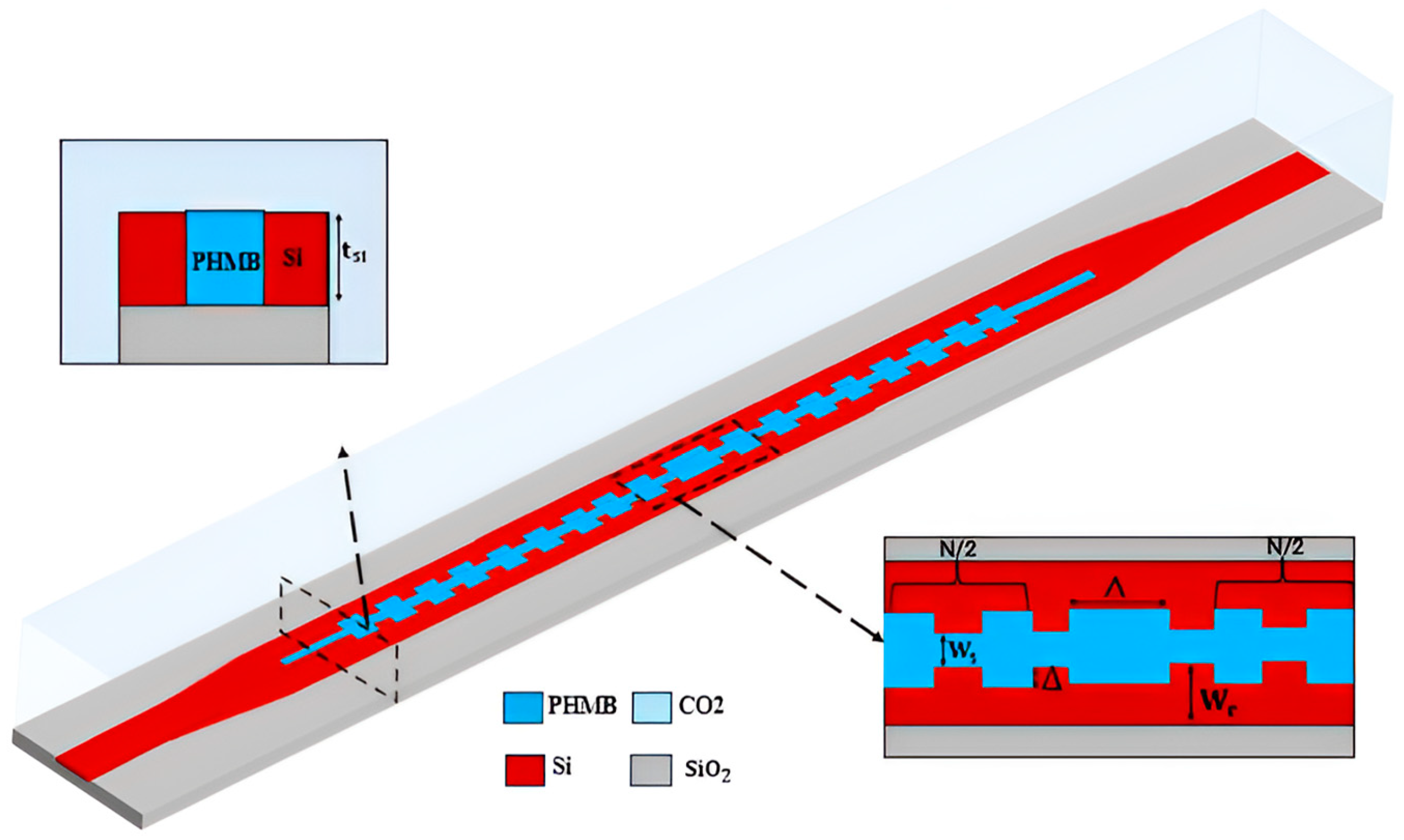
As shown in Figure 1, the proposed SP-PSBG is designed on a SOI platform with a 2 µm silicon dioxide () substrate. The structure consists of two silicon rails separated by a low-index slot region. A PHMB-filled slot is introduced between the two rails, with a thickness equal to that of the silicon layer, 220 nm. This configuration facilitates the penetration of molecules deeper into the functional material, hence improving light–gas interaction and sensing efficiency. The SP-PSBG’s geometric parameters include a slot width () of 100 nm and a silicon rail width () of 230 nm. The Bragg gratings are implemented by introducing periodic sidewall corrugations inside the slot waveguide, with a corrugation depth () of 12 nm. A central defect region is introduced in the center of the grating, creating a phase shift that enhances the resonant properties of the device. The length of the phase shift is intended to be equivalent to one grating period (∧) and is carefully engineered to achieve a Bragg wavelength near 1550 nm. The grating period is optimized based on the effective refractive index calculated at this wavelength. On each side of the phase shift, there are N/2 grating segments, where N is the total number of grating periods arranged symmetrically around the defect. The device comprises 80 grating periods, resulting in a total length of 38.2 µm, making it well-suited for miniaturized sensing applications.

Figure 1.
Structure diagram of proposed phase shift Bragg grating slot waveguide.
A transverse electric (TE) mode source is injected through a strip-to-slot mode converter, which utilizes multimode interference (MMI) to efficiently transform the strip mode into a slot mode. Using power splitting, the converter smoothly and gradually couples the mode into the slot, ensuring a seamless transition. This design achieves a high propagation efficiency of approximately 98% while maintaining a compact footprint [33].
2.2. Theoretical Model
Bragg gratings exploit periodic RI modulations to reflect light at a specific wavelength, known as the Bragg wavelength . The fundamental condition governing Bragg gratings is given by [34]:
Under this condition, the reflection of light from successive grating planes interferes constructively, resulting in the formation of a photonic bandgap that prevents light propagation over a specific spectral range. To create a narrowband resonance within the photonic bandgap, a segment with a length equal to a single grating period is introduced, enabling a /4 phase shift at the target wavelength. The effective optical path length across one period is governed by the following relation:
where and represent the effective indices of the two alternating sections within the grating structure, while and denote the lengths of the wide and narrow sections, respectively. The duty cycle is chosen to be 50%, meaning that the grating lengths are equal ( = = /2). This balanced distribution ensures optimal coupling efficiency and phase matching.
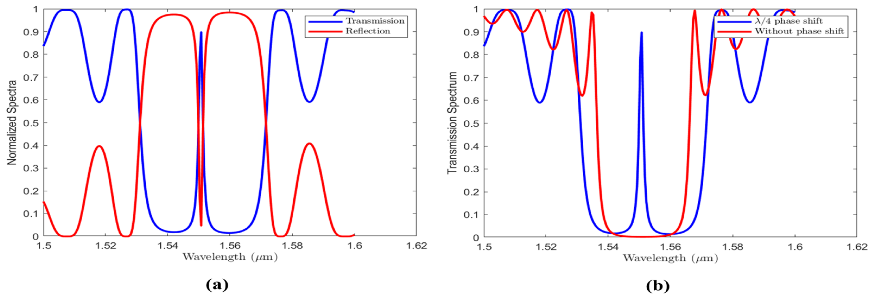
Figure 2a presents the simulated transmission and reflection spectra of the SP-PSBG; the structure efficiently reflects wavelengths within the photonic bandgap, while allowing strong transmission at the defect mode. Figure 2b illustrates the spectral response of the SP-PSBG with and without a defect. In contrast to a traditional Bragg grating, the addition of a /4 phase shift causes a resonance within the photonic bandgap, producing a strong transmission peak and greatly expanding the bandwidth. SP-PSBG modifies the spectral response by introducing an additional resonance within the photonic bandgap, leading to a broadened transmission window. Mathematically, the bandwidth of a PSBG is given by the following equation:
where ng is the group index and is the coupling coefficient representing the strength of mode coupling due to the refractive index modulation within the grating region. Defined as , it is directly related to the index contrast and has units of cm−1. This additional term arises from the resonance condition imposed by the phase-shifted cavity, analogous to a Fabry–Pérot resonance. It reflects the quantization of the defect mode supported within the full grating length L and contributes to the overall bandwidth enhancement beyond the traditional limited Bragg grating [35].
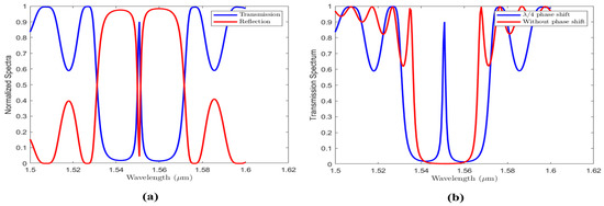
Figure 2.
Normalized spectra: (a) transmission and reflection spectra of SP-PSBG; (b) transmission spectrum of SP-PSBG (/4 phase shift) and BG (without phase shift).
The confinement factor of the mode within the slot determines the fraction of optical power localized in the low-index region. It is expressed as follows:
where is the confinement factor and represents the electric field intensity. A higher confinement factor indicates stronger localization of the mode within the slot, which enhances light–matter interactions.
3. Structural Optimization Based on Maximizing the Confinement Factor
The SP-PSBG was designed and analyzed using the Lumerical finite-difference time domain (FDTD) simulation tool. Perfectly matched layer (PML) boundary conditions with 12 layers were applied in all directions to effectively absorb outgoing waves and minimize reflections at the simulation boundaries. An override mesh with a step size of 50 nm was implemented in the y-direction to accurately capture the small variations in the grating depth. An integer number of periods was used for the mesh size in the x-direction, which is the propagation direction, and a mesh size of 200 nm was sufficient in the z-direction. A TE-mode wave source was employed, with a wavelength range from 1500 to 1600 nm. Lumerical’s integrated silicon and Silica material models were used in the simulations. Furthermore, without gas, the RI of PHMB is 1.55 at a wavelength of 1550 nm. Figure 3 illustrates the simulated electric field distribution within the designed SP-PSB structure. In Figure 3a, the cross-sectional view in the yz-plane illustrates the electric field intensity distribution for the TE-polarized mode. The optical field is strongly confined within the low-index slot region, demonstrating strong lateral confinement. Figure 3b presents the corresponding field distribution for the TM-polarized mode, which exhibits a broader field spread and vertical component. This behavior indicates weaker confinement within the slot and highlights the polarization sensitivity of the structure.
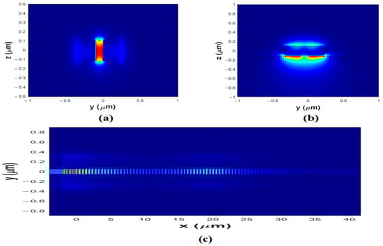
Figure 3.
The electric field distribution in the SP-PSBG structure. (a) The electric field intensity of the TE mode in the yz-plane. (b) The electric field distribution of the TM mode in the yz-plane. (c) The lateral electric field distribution in the xy-plane.
Figure 3c illustrates the distribution of the lateral electric field along the direction of propagation. The input mode, entering from the left, is partially reflected by the periodic grating. The gratings facilitate constructive and destructive interference through Bragg reflection, which progressively reduces the forward-propagating field and produces strong reflective feedback. In the center of the waveguide, a portion of the input light resonates within this cavity, resulting in a narrow transmission peak at the corresponding resonant wavelength. To optimize the dimensions of the SP-PSBG, the approach focuses on maximizing the confinement of the TE mode within the polymer slot. This enhancement of light–matter interaction ultimately improves the performance of the device.
3.1. The Effect of Rail Width
The rail width is an important parameter in enhancing the sensor’s sensitivity by controlling how strongly the optical mode is confined within the low-index slot. A higher Γ leads to stronger light–matter interaction, which is important for enhancing the sensing performance. To analyze this effect, we employed the Finite-Difference Eigenmode (FDE) solver in Lumerical to compute the RI of the grating planes and the Γ of the TE mode for various values of , while keeping other design parameters fixed. Specifically, was set to 100 nm, to 12 nm, ∧ to 471 nm, and N to 80. Figure 4 illustrates the variation of the Γ and the with . As the increases, the Γ decreases, indicating weaker confinement in the low-index PHMB slot. At the same time, the increases due to greater mode overlap with the high-index silicon. Consequently, designs that incorporate narrower values are more likely to achieve higher sensitivity. Based on our simulations, selecting a of approximately 230 nm will maximize the Γ within the slot.
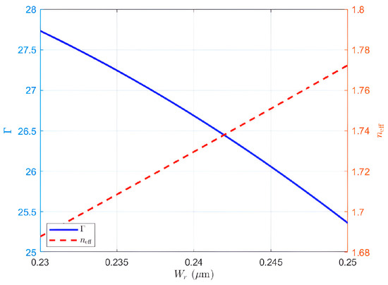
Figure 4.
Variation of confinement factor and effective RI across different rail widths.
3.2. The Effect of Slot Width
While choosing a of 230 nm can maximize sensitivity, we need to study the effect of under the same parameters. Figure 5a shows how the variation in affects both Γ and . The downward trend of the Γ indicates that as the increases, the optical mode becomes less confined within the low-index region, suggesting that a narrower is preferable for enhanced sensitivity. However, when the decreases, the effective RI rises, increasing the propagation loss. Figure 5b presents the transmission spectra for different values, showing that reducing the enhances the Γ but simultaneously increases propagation loss due to the rise in the effective RI. To solve this trade-off, we select a of 100 nm, achieving a narrow FWHM of 1 nm and a transmission peak of 0.9.
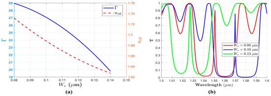
Figure 5.
Effect of on Γ, , and transmission characteristics. (a) Variation of Γ and as function of . (b) Transmission spectra for different values of .
3.3. The Effect of Number of Grating
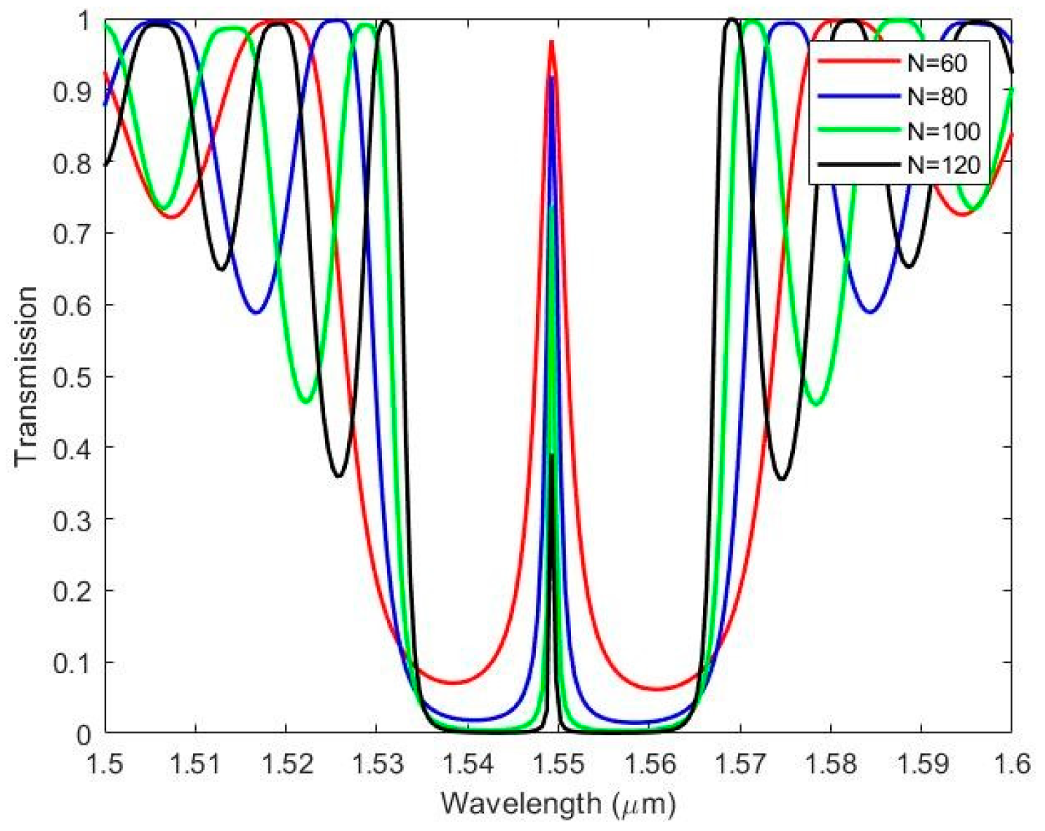
The transmission spectra for different numbers of gratings are presented in Figure 6, while maintaining a of 100 nm and keeping all other parameters constant. As the number of gratings increases, the coupling coefficient improves due to stronger interaction between the waveguide mode and the grating structure. This leads to a sharper and more defined resonance, resulting in an enhancement in the FWHM. However, increasing the number of gratings also introduces additional scattering and absorption, contributing to greater propagation loss. Therefore, a trade-off must be considered between achieving higher confinement and maintaining low loss. Based on these observations, 80 gratings were chosen as the optimal configuration, providing a suitable balance between enhanced optical confinement and minimal propagation loss.
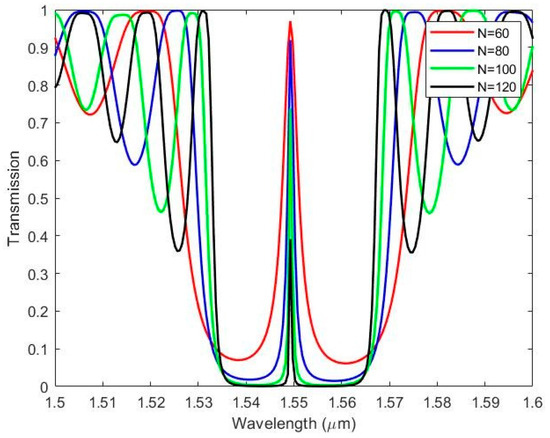
Figure 6.
Transmission spectra for different number of gratings.
3.4. The Effect of Gratings Depth
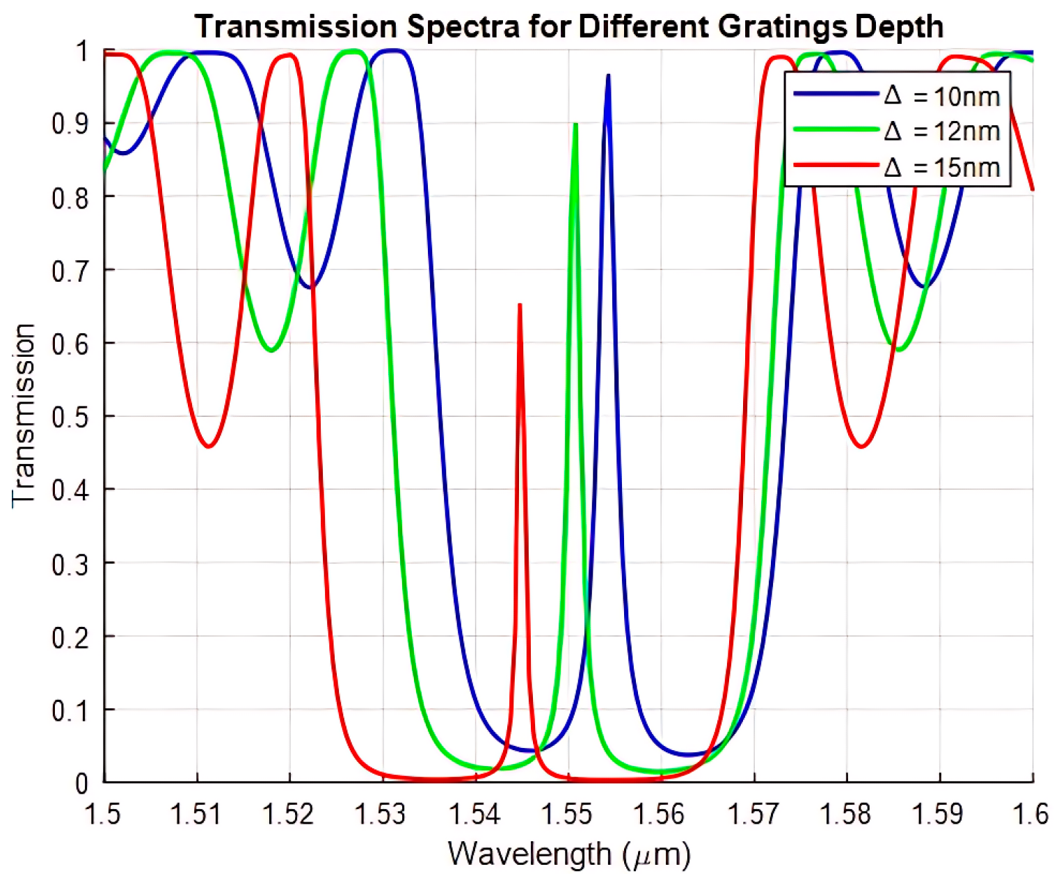
The effect of increasing the grating depth while maintaining a fixed number of grating periods (80) is investigated in Figure 7. Increasing the depth leads to sharper peak transmission as the mode will be more confined in the PHMB slot but also results in significant propagation loss due to the increase in . On the other hand, a small depth provides a high peak with a broad FWHM. Choosing a of 12 nm can resolve this trade-off, providing a narrow peak with an FWHM of 1.6 nm and a high peak transmission of 0.9. With this configuration, propagation losses are kept to a minimum, while the sensor maintains a sharp resonance. Furthermore, moderate grating depths increase fabrication tolerance, strengthening the structure against alignment errors and etching variations.
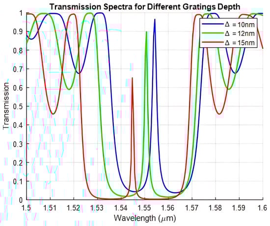
Figure 7.
Transmission spectra for different grating depths.
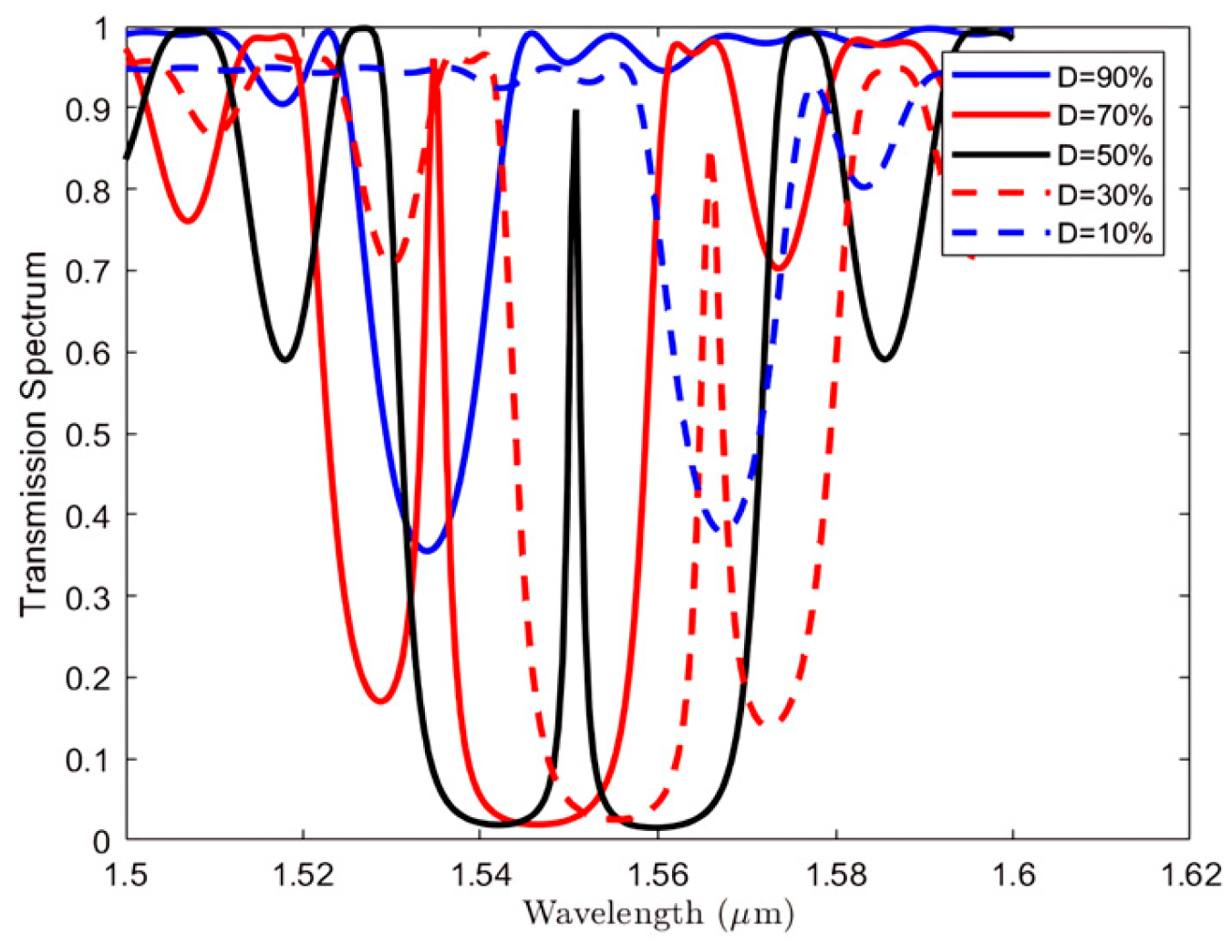
3.5. The Effect of Duty Cycle
The transmission spectrum of the SP-PSBG exhibits a strong dependence on the duty cycle (D). As shown in Figure 8, transmission responses around D = 50% are similar, primarily differing in their spectral position. A duty cycle of 50% provides the most effective confinement of the resonance peak within the band gap, resulting in an optimal transmission response.
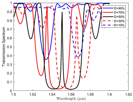
Figure 8.
Transmission spectra for different grating duty cycles.
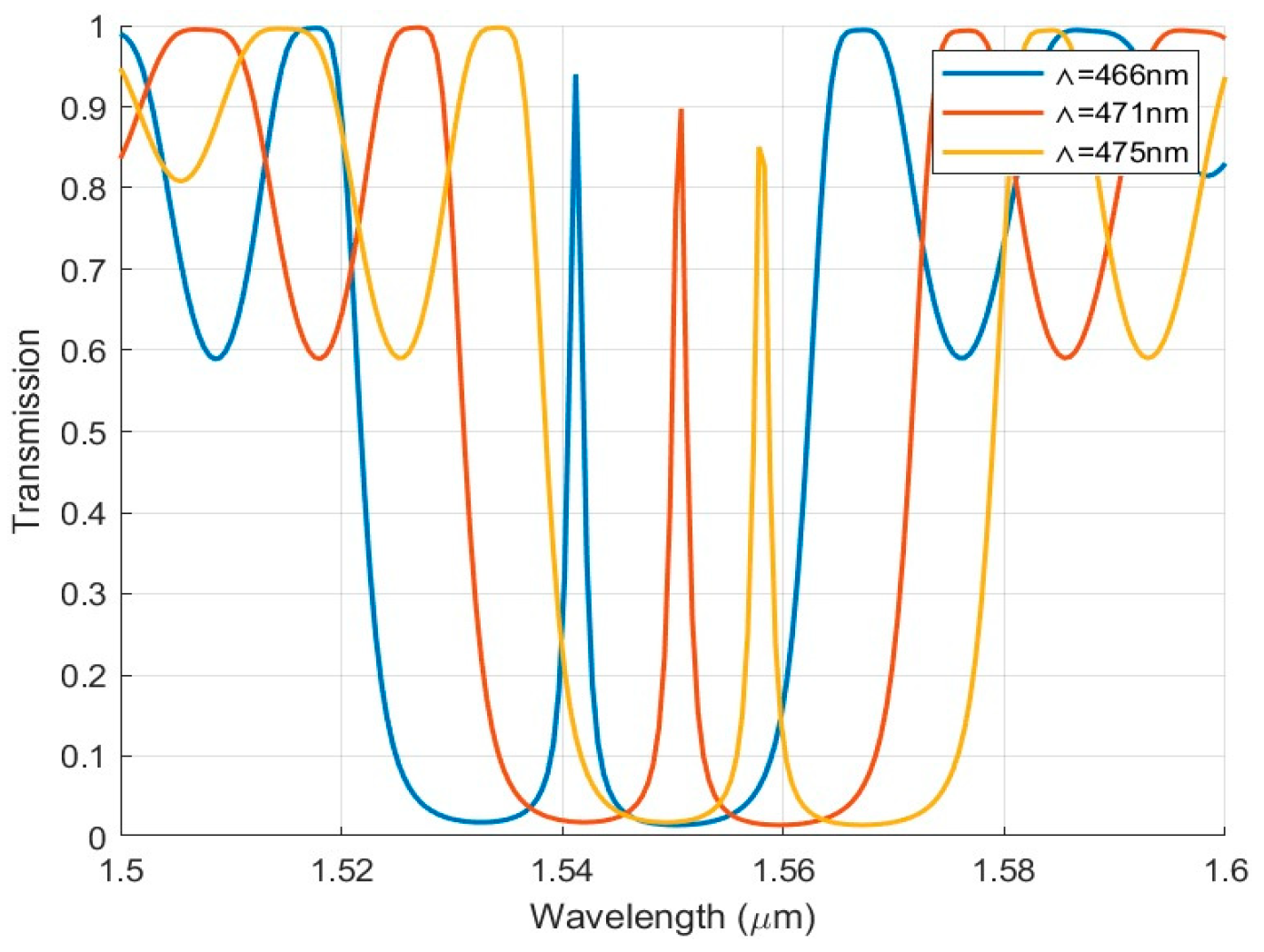
3.6. The Effect of Grating Period
The transmission spectra for various values of , with all other design parameters kept constant, are shown in Figure 9. As observed, increasing the grating period causes the resonance dips to shift toward longer wavelengths (redshift), while a smaller period results in a blueshift. Our goal is to achieve a resonance wavelength of 1.55 µm in the absence of gas concentration, which can be obtained by selecting a ∧ of 471 nm.
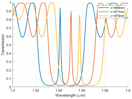
Figure 9.
Transmission spectra for different grating periods.
4. Performance Evaluation of the SP-PSBG for Detection
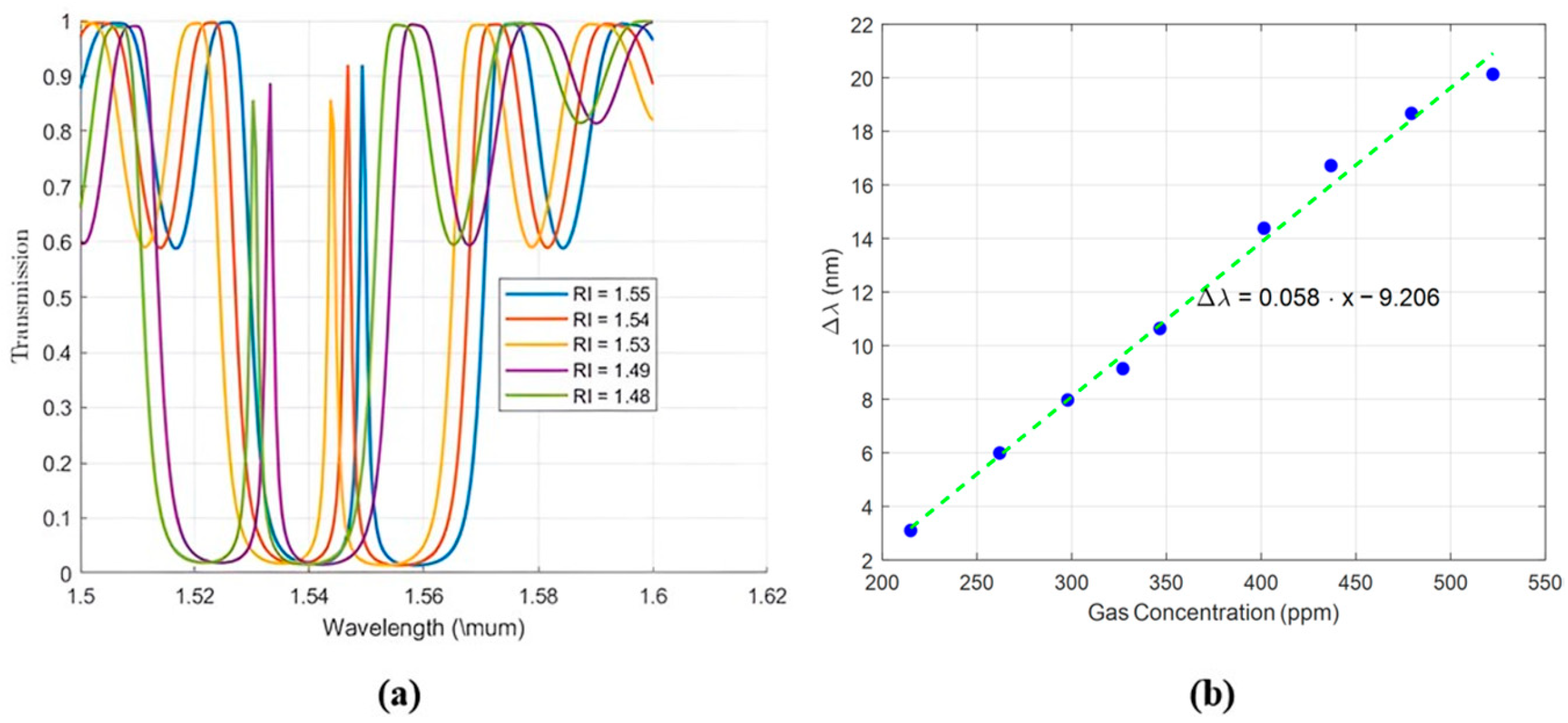
In this section, the RI sensing performance of SP-PSBG will be further examined using the optimal device parameters obtained above. The proposed sensor operates based on the concentration-dependent variation of the RI of PHMB, which is influenced by the presence of gas. The transmission spectrum shifts toward shorter wavelengths (blueshift) as the concentration increases due to a decrease in the RI of the PHMB material. In the absence of , the RI of PHMB is approximately 1.55. A small drop of 0.01 in the RI causes the resonance wavelength to shift to 1.547 µm, as illustrated in Figure 10a. As the concentration rises to 215, 262, and 328 ppm, the RI of PHMB decreases further to 1.54, 1.53, and 1.52, respectively. This trend continues up to a concentration of 524 ppm, where the RI reaches values as low as 1.48. The reduction in RI alters the effective RI of the device, significantly enhancing its sensitivity to gas concentration changes.

Figure 10.
SP-PSBG performance evaluation. (a) Response of proposed gas sensor under different concentrations. (b) Relationship between shift in and gas concentration.
The sensitivity of the sensor is determined by monitoring the shift in the resonant wavelength for different gas concentrations. Optical sensors with high sensitivity are essential for detecting trace levels of gases. The sensitivity is calculated using the following equation:
where represents the wavelength shift in ppm and . denotes the change in gas centration in ppm. Using this relation, a refractive index changes of 215 ppm (e.g., from 0 ppm to 215 ppm) resulted in a wavelength shift of approximately 3.1 nm, which is equivalent to 3100 pm. This corresponds to a sensitivity of 3100 pm/215 ppm ≈ 14.4 pm/ppm. This result demonstrates that the sensor is highly responsive to variations in concentration, making it well-suited for precise gas detection applications. To further evaluate the sensor’s performance, we calculate the , which quantifies the trade-off between sensitivity and spectral resolution. The is defined as follows:
A higher indicates better sensing performance, as it signifies strong sensitivity with minimal spectral broadening. For our device, we obtained an of 9 × , highlighting its capability for high-precision gas sensing. Figure 10b illustrates that the wavelength shift exhibits a linear trend within the concentration range of 215 ppm to 500 ppm, confirmed by applying best line fitting. Achieving linear sensitivity is a crucial characteristic of the sensor, as it ensures consistent and predictable performance across different gas concentrations. Other studies on PHMB polymer sensors have also highlighted the importance of linearity in sensor response, further supporting its relevance in ensuring accurate detection across varying concentrations [30,31].
Finally, we compare our device with other optical designs based on PHMB polymer material. As shown in Table 1, our SP-PSBG-based design outperforms previous silicon photonic works by improving both sensitivity and , demonstrating its superior performance in gas sensing applications. We have also included recent plasmonic-based sensors that utilize PHMB in their functional layers to provide a broader context. Although some plasmonic structures offer high sensitivity (>100 pm/ppm), their use of metallic elements can increase optical losses and hinder integration with standard photonic circuits. Our silicon-based design effectively balances sensitivity, spectral resolution, and the practicality of fabrication. To further enhance device sensitivity, sub-100 nm slot waveguides can be employed to increase the evanescent field overlap with the analyte. Additionally, exploring alternative functional materials with higher affinity and selectivity for may further improve detection performance.

Table 1.
Comparison of this study with previous studies.
5. Future Work
The proposed waveguide sensor is designed using standard SOI technology, making it suitable for fabrication using conventional CMOS-compatible processes. Specifically, the design is compatible with the IMEC passive silicon photonics platform accessed via the SiEPIC foundry service, which utilizes 200 mm SOI wafers with a 220 nm silicon device layer over a 2 µm buried oxide. The fabrication process is based on 193 nm deep ultraviolet (DUV) lithography and dry etching, enabling precise definition of sub-100 nm features such as narrow slot waveguides and finely patterned Bragg grating [37,38]. This technology ensures high uniformity and scalability, which are essential for reliable large-scale production. To validate the real-world performance of the sensor, we have submitted the design for fabrication as part of our future work.
The current design operates in the near-infrared region, using the low absorption and high refractive index contrast of silicon at telecom wavelengths. However, the design concept is not limited to this spectral range. With appropriate modifications, particularly replacing silicon with a low-loss material such as silicon nitride , the structure can be adapted for operation in the visible range. shows low optical absorption in the visible spectrum and is compatible with CMOS fabrication processes. The waveguide dimensions would have to be scaled appropriately to guarantee effective mode confinement at shorter wavelengths. Furthermore, by tailoring the functional material coatings, the platform can be adapted for various sensing applications, enabling versatility in both wavelength tuning and target analyte detection.
6. Conclusions
In this study, we introduced a novel gas sensor based on a SP-PSBG waveguide filled with PHMB as the sensing medium. Our numerical simulations demonstrate a high sensitivity of 14.4 pm/ppm and a sharp FWHM of 1.6 nm, outperforming conventional polymer-coated gas sensors. The innovation of our design lies in the direct interaction between the PHMB-filled resonance structure and the surrounding particles, eliminating the need for a coating layer of PHMB and effectively improving light–analyte interaction. This sensor is highly suitable for real-time and low-concentration gas sensing applications.
Author Contributions
Conceptualization and proposing the idea, M.A.S.; data curation, P.H.; formal analysis, M.K. (Merna Khafagy); investigation, P.H.; methodology, M.K. (Merna Khafagy) and M.K. (Maira Khafagy); resources, M.K. (Merna Khafagy) and P.H.; software, M.K. (Merna Khafagy) and M.K. (Maira Khafagy); supervision, M.A.S.; validation, M.K. (Merna Khafagy); writing—original draft, M.K. (Maira Khafagy); writing—review and editing, M.A.S. All authors have read and agreed to the published version of the manuscript.
Funding
This research received no external funding.
Institutional Review Board Statement
Not applicable.
Informed Consent Statement
Not applicable.
Data Availability Statement
The original contributions presented in this study are included in the article. Further inquiries can be directed to the corresponding author(s).
Acknowledgments
The authors would like to acknowledge partial support from the AFRETEC research fund.
Conflicts of Interest
The authors declare no conflict of interest.
References
- Qu, H.; Duan, X. Recent advances in micro detectors for micro gas chromatography. Sci. China Mater. 2019, 62, 611–623. [Google Scholar] [CrossRef]
- Rindelaub, J.; Wiley, J.; Cooper, B.; Shepson, P. Chemical characterization of -pinene secondary organic aerosol constituents using gas chromatography, liquid chromatography, and paper spray-based mass spectrometry techniques: Characterization of -pinene SOA constituents. Rapid Commun. Mass Spectrom. 2016, 30, 1627–1638. [Google Scholar] [CrossRef]
- Shaaban, H.; Mostafa, A.; Górecki, T. Green Gas and Liquid Capillary Chromatography. In The Application of Green Solvents in Separation Processes; Elsevier: Amsterdam, The Netherlands, 2017. [Google Scholar]
- McNair, H.; Miller, J.; Snow, N. Basic Gas Chromatography; Wiley: Hoboken, NJ, USA, 2019. [Google Scholar]
- Bogue, R. Detecting gases with light: A review of optical gas sensor technologies. Sens. Rev. 2015, 35, 133–140. [Google Scholar] [CrossRef]
- Butt, M.A.; Piramidowicz, R. Integrated photonic sensors for the detection of toxic gasses—A review. Chemosensors 2024, 12, 143. [Google Scholar] [CrossRef]
- Jahromi, H.D.; Kazemi, M.; Sheikhi, M.H. Room temperature and highly sensitive acetone sensor based on lead sulfide nanosheets. Mater. Sci. Eng. B 2021, 267, 115082. [Google Scholar] [CrossRef]
- Mosahebfard, A.; Jahromi, H.D.; Sheikhi, M.H. Highly Sensitive, Room Temperature Methane Gas Sensor Based on Lead Sulfide Colloidal Nanocrystals. IEEE Sens. J. 2016, 16, 4174–4179. [Google Scholar] [CrossRef]
- Zheng, S.; Ghandehari, M.; Ou, J. Photonic crystal fiber long-period grating absorption gas sensor based on a tunable erbium-doped fiber ring laser. Sens. Actuators B Chem. 2016, 223, 324–332. [Google Scholar] [CrossRef]
- Antonacci, G.; Goyvaerts, J.; Zhao, H.; Baumgartner, B.; Lendl, B.; Baets, R. Ultra-sensitive refractive index gas sensor with functionalized silicon nitride photonic circuits. APL Photonics 2020, 5, 081301. [Google Scholar] [CrossRef]
- Bakshi, B.; Varshney, R.K.; Pal, B.P. Silicon photonics-based gas sensors and components for the Mid-IR: Design and Modelling. In Proceedings of the ICOL-2019, International Conference on Optics and Electro-Optics, Dehradun, India, 19–22 October 2019; Springer: Berlin/Heidelberg, Germany, 2021; pp. 7–10. [Google Scholar]
- Chrostowski, L.; Hochberg, M. Silicon Photonics Design: From Devices to Systems; Cambridge University Press: Cambridge, UK, 2015. [Google Scholar]
- Tsigaridas, G.N. A study on refractive index sensors based on optical micro-ring resonators. Photonic Sens. 2017, 7, 217–225. [Google Scholar] [CrossRef]
- Gerguis, J.O.; Qi, M. Linear and passive silicon-on-insulator refractive index sensor utilizing Bragg grating-assisted Michelson interferometer. Opt. Express 2025, 33, 9102–9116. [Google Scholar] [CrossRef]
- Lotfiani, A.; Jahromi, H.D. Guided-Mode Resonance Enhanced Ge-on-Si Self-Powered Surface Illuminated Photodetector for Ultrahigh-Speed Optical Communication Systems. IEEE Sens. J. 2024, 24, 40669–40677. [Google Scholar] [CrossRef]
- Izadpour, A.R.; Jahromi, H.D.; Sheikhi, M.H. Plasmonic Enhancement of Colloidal Quantum Dot Infrared Photodetector Photosensitivity. IEEE J. Quantum Electron. 2018, 54, 7200207. [Google Scholar] [CrossRef]
- Wu, Y.; Zhou, Y.; Pan, J.; Huang, T.; Jin, S. Design of highly sensitive refractive index sensor based on silicon photonic Mach–Zehnder interferometer. Opt. Commun. 2023, 534, 129288. [Google Scholar] [CrossRef]
- Zhao, C.; Chen, P.; Zhang, L. Numerical analysis of effective refractive index sensor based on slot micro-ring and Bragg grating. Int. J. Mod. Phys. B 2019, 33, 1950292. [Google Scholar] [CrossRef]
- Fernández Gavela, A.; Grajales García, D.; Ramirez, J.C.; Lechuga, L.M. Last advances in silicon-based optical biosensors. Sensors 2016, 16, 285. [Google Scholar] [CrossRef]
- Salama, N.A.; Alexeree, S.M.; Obayya, S.S.; Swillam, M.A. Silicon-based double fano resonances photonic integrated gas sensor. Sci. Rep. 2024, 14, 24811. [Google Scholar] [CrossRef]
- Liu, C.; Wang, J.; Wu, X.; Sun, X.; Qiao, Z.; Xin, Y.; Zhang, J. Design and optimization of asymmetric grating assisted slot Microring. Photonics 2022, 9, 988. [Google Scholar] [CrossRef]
- Liu, C.; Sang, C.; Wu, X.; Cai, J.; Wang, J. Grating double-slot micro-ring resonator for sensing. Opt. Commun. 2021, 499, 127280. [Google Scholar] [CrossRef]
- Koushik, K.P.; Malathi, S. Optical micro-ring resonator for detection of carbon dioxide gas. In Emerging Trends in Photonics, Signal Processing and Communication Engineering: Proceedings of ICPSPCT 2018, Bangalore, India, 18–20 July 2018; Springer: Berlin/Heidelberg, Germany, 2020; pp. 157–161. [Google Scholar]
- Dehdashti Jahromi, H. Performance analysis of transmissive modified cladding optical fibre sensors. IET Optoelectron. 2022, 16, 63–71. [Google Scholar] [CrossRef]
- Khonina, S.; Kazanskiy, N.; Butt, M.A.; Kaz’mierczak, A.; Piramidowicz, R. Plasmonic sensor based on metal-insulator-metal waveguide square ring cavity filled with functional material for the detection of CO2 gas. Opt. Express 2021, 29, 16584–16594. [Google Scholar] [CrossRef]
- Butt, M.; Kazanskiy, N.; Khonina, S. On-chip symmetrically and asymmetrically transformed plasmonic Bragg grating formation loaded with a functional polymer for filtering and CO2 gas sensing applications. Measurement 2022, 201, 111694. [Google Scholar] [CrossRef]
- Zeng, L.; Li, B.; Wen, R.; Zhang, X. Plasmonic Sensor Based on Multi Fano Resonance in Inverse T Shape Structure for Detection of CO2 Concentration. IEEE Photonics J. 2023, 15, 1–5. [Google Scholar] [CrossRef]
- Long, W.; Zhou, R.; Du, Z.; Ling, Q.; Zhang, Y.; Zhao, D.; Shao, J.; Luo, S.; Chen, D. A Dual-Band Carbon Dioxide Sensor Based on Metal–TiO2–Metal Metasurface Covered by Functional Material. Photonics 2022, 9, 855. [Google Scholar] [CrossRef]
- Reed, G.T.; Mashanovich, G.; Gardes, F.Y.; Thomson, D. Silicon optical modulators. Nat. Photonics 2010, 4, 518–526. [Google Scholar] [CrossRef]
- Mi, G.; Horvath, C.; Van, V. Silicon photonic dual-gas sensor for H2 and CO2 detection. Opt. Express 2017, 25, 16250–16259. [Google Scholar] [CrossRef]
- Mi, G.; Horvath, C.; Aktary, M.; Van, V. Silicon microring refractometric sensor for atmospheric CO2 gas monitoring. Opt. Express 2016, 24, 1773–1780. [Google Scholar] [CrossRef]
- Badri, S.H. Transmission resonances in silicon subwavelength grating slot waveguide with functional host material for sensing applications. Opt. Laser Technol. 2021, 136, 106776. [Google Scholar] [CrossRef]
- Deng, Q.; Yan, Q.; Liu, L.; Li, X.; Michel, J.; Zhou, Z. Robust polarization-insensitive strip-slot waveguide mode converter based on symmetric multimode interference. Opt. Express 2016, 24, 7347–7355. [Google Scholar] [CrossRef]
- Kulkarni, M.R.; Manoj Kumar, B.; Malghan, M.M.; Mohamedarif, G.; Honnungar, R.V. Planar Waveguide Bragg Grating Pressure Sensor—Design and Applications. In Emerging Trends in Photonics, Signal Processing and Communication Engineering: Proceedings of ICPSPCT 2018, Bangalore, India, 18–20 July 2018; Springer: Berlin/Heidelberg, Germany, 2020; pp. 53–62. [Google Scholar]
- Husko, C.; Ducharme, A.; Fahrenkopf, N.M.; Guest, J.R. Phase-shifted Bragg gratings in a foundry silicon nitride platform. OSA Contin. 2021, 4, 933–939. [Google Scholar] [CrossRef]
- Li, H.; Sun, B.; Yuan, Y.; Yang, J. Guanidine derivative polymer coated microbubble resonator for high sensitivity detection of CO2 gas concentration. Opt. Express 2019, 27, 1991–2000. [Google Scholar] [CrossRef]
- Wang, X.; Grist, S.; Flueckiger, J.; Jaeger, N.A.; Chrostowski, L. Silicon photonic slot waveguide Bragg gratings and resonators. Opt. Express 2013, 21, 19029–19039. [Google Scholar] [CrossRef] [PubMed]
- Wang, X.; Shi, W.; Vafaei, R.; Jaeger, N.A.; Chrostowski, L. Silicon-on-insulator Bragg gratings fabricated by deep UV lithography. In Proceedings of the Asia Communications and Photonics Conference and Exhibition, Shanghai, China, 8–12 December 2010; pp. 501–502. [Google Scholar]


Disclaimer/Publisher’s Note: The statements, opinions and data contained in all publications are solely those of the individual author(s) and contributor(s) and not of MDPI and/or the editor(s). MDPI and/or the editor(s) disclaim responsibility for any injury to people or property resulting from any ideas, methods, instructions or products referred to in the content. |
© 2025 by the authors. Licensee MDPI, Basel, Switzerland. This article is an open access article distributed under the terms and conditions of the Creative Commons Attribution (CC BY) license (https://creativecommons.org/licenses/by/4.0/).