Communication

A 1 × 4 Silica-Based GMZI Thermo-Optic Switch with a Wide Bandwidth and Low Crosstalk

Professional Basic Teaching Department, Changchun Polytechnic University, Changchun 130033, China
Photonics 2025, 12(7), 721; https://doi.org/10.3390/photonics12070721
Submission received: 29 April 2025 / Revised: 18 June 2025 / Accepted: 15 July 2025 / Published: 16 July 2025
(This article belongs to the Special Issue Advances in Integrated Photonics)

Abstract

The growing demand for communication capacity has driven advancements in optical switches. However, measurement procedures for large-scale switching arrays become more complex as the number of units increases. Multi-port optical switches can reduce the measurement complexity. In this work, we demonstrate a 1 × 4 thermo-optic switch fabricated on a silica platform, based on a Generalized Mach–Zehnder Interferometer (GMZI) structure with a wide bandwidth and low crosstalk. The device enables flexible switching among four output channels, achieving a crosstalk below −15 dB over the 1500–1580 nm wavelength range and an insertion loss of −6.51 dB at 1550 nm.

1. Introduction

Driven by emerging technologies such as 5G networks, cloud computing, artificial intelligence (AI), and the Internet of Things (IoT), global data traffic is growing exponentially, posing new challenges to bandwidth, speed, and transmission distance in communication systems [1,2,3]. Due to the shortcomings of traditional electrical communication in these aspects, optical communication is increasingly replacing electrical communication and becoming the backbone network in communication systems [4]. Optical switches, as an important component in optical communication networks, can realize the dynamic routing of optical signals, signal monitoring, and network reconfiguration [5]. Compared to micro-electromechanical system (MEMS) switches [6], waveguide optical switches have faster response speeds and more compact structural dimensions, making them more suitable for large-scale integration, and they have also been verified on many material platforms. The silicon nitride platform exhibits extremely low propagation loss and high-power tolerance, but its excellent thermal stability results in relatively high modulation power for thermo-optic devices [7]. The lithium niobate platform possesses strong nonlinear effects and stable optical performance, yet its higher optical loss remains an issue to be addressed [8]. The polymer platform features a high thermo-optic coefficient and simple fabrication processes, making it suitable for thermo-optic switches [9]; however, the low material stability of polymers limits their long-term operation. The silicon photonics (SiPh) platform is compatible with existing complementary metal–oxide–semiconductor (CMOS) processes, enabling the efficient development of optical devices, while its high refractive index contrast allows for reduced device dimensions [10]. However, the smaller waveguide size decreases the fabrication tolerance, and the propagation loss becomes highly sensitive to waveguide sidewall roughness. Silica Planar Lightwave Circuits (PLCs) are also CMOS-compatible and have achieved commercialization due to their mature fabrication technology and superior stability. With high fabrication tolerance, low propagation loss, and well-established edge coupling techniques, they serve as an excellent photonic platform [11].
In recent years, various large-scale switch arrays have been proposed, with the largest scale reaching 128 ports [12]. Whether based on MZI [13,14], asymmetric Mach–Zehnder interferometer (AMZI) [15], or microring resonator (MRR) [16] structures, the fundamental building blocks of these arrays are 1 × 2 or 2 × 2 switches. Inevitable fabrication errors necessitate the calibration of each unit’s operating voltage, while the large number of switching elements further increases chip size, power consumption, and measurement complexity. Multi-port switch units offer a potential solution to this challenge. In this paper, we present a 1 × 4 thermo-optic (TO) switch based on a GMZI structure on a silica platform, featuring a broad operating bandwidth and low crosstalk. Across an 80 nm bandwidth, the crosstalk remains below −15 dB, with an insertion loss of less than −6.51 dB.

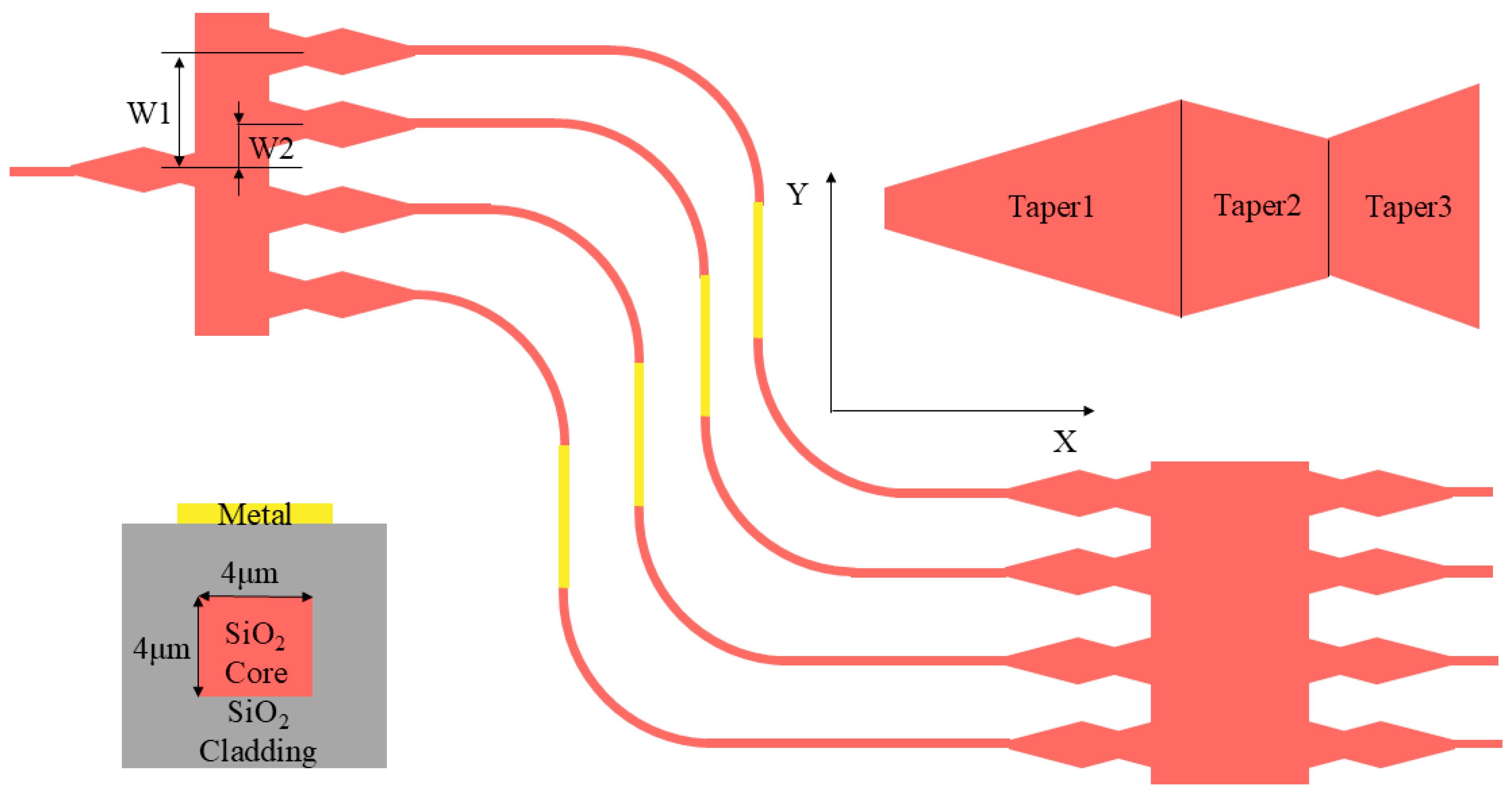
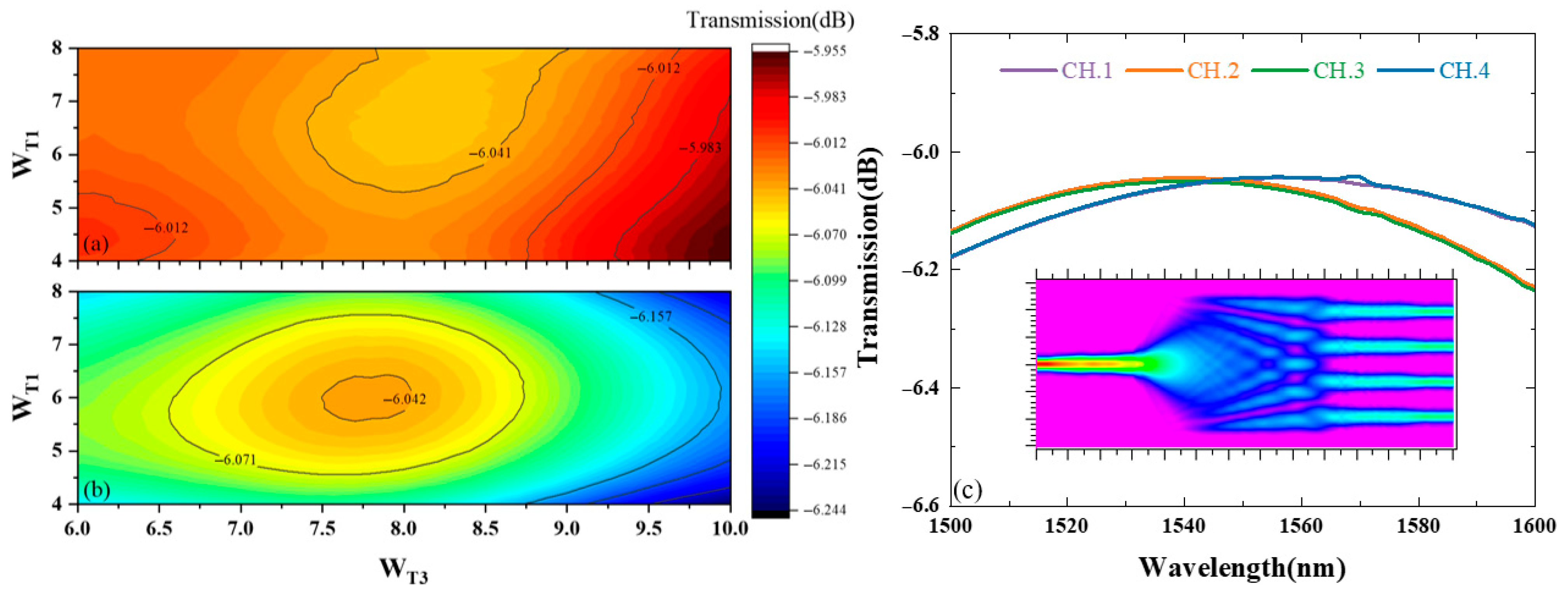
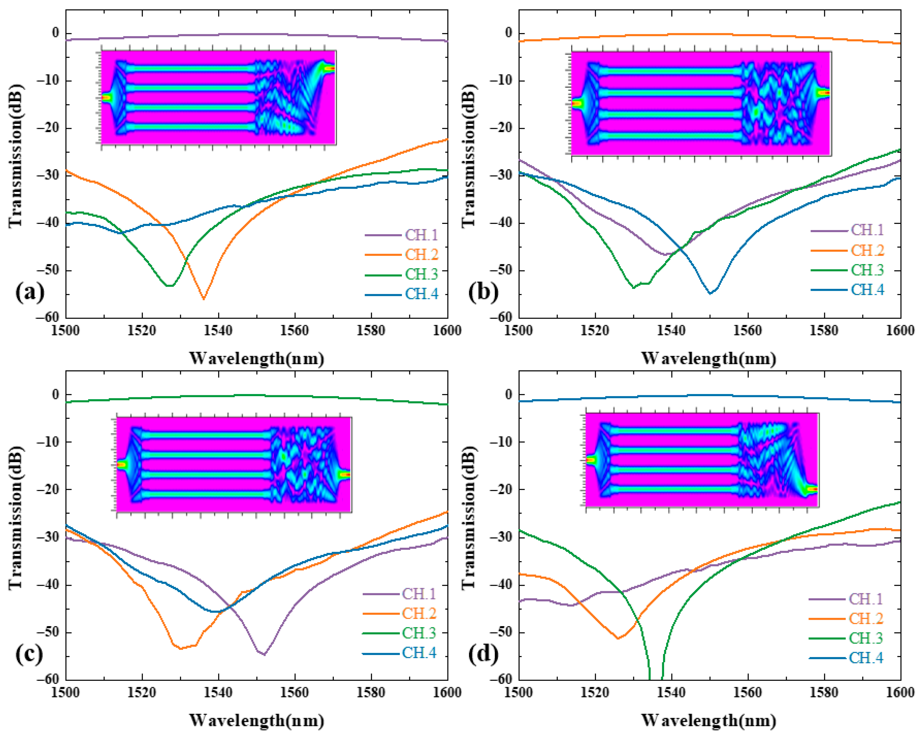
2. Design and Simulation

The cross-section of the designed waveguide is shown in the lower left corner of Figure 1, consisting of a silica cladding (refractive index = 1.4448@1550 nm) and a silica core layer (refractive index = 1.4737@1550 nm), with metal electrodes positioned above. To achieve single-mode propagation in the waveguide with a refractive index contrast of 1.94%, the core dimensions were set to 4 μm × 4 μm. This device functions as a TO switch, where Joule heating from the metal electrodes induces a refractive index change in the material. The change in the material’s refractive index will alter the waveguide’s effective refractive index, thereby affecting the interference in the MMI and consequently influencing the path switching of the switch. In conventional N × N non-cascading switch designs, additional waveguide length is introduced to increase the spacing between TO phase shifters, thereby reducing the thermal crosstalk. However, this approach inevitably introduces excess phase variations, resulting in both narrowed operational bandwidth and increased crosstalk levels [7]. Our proposed GMZI structure employs two circular arcs with identical curvature directions to connect the phase shifters. This design ensures equal arm lengths while simultaneously reducing thermal crosstalk between waveguides without introducing additional phase variations, thereby broadening the device’s operational bandwidth. As illustrated in Figure 1, the GMZI structure consists of a 1 × 4 multimode interferometer (MMI) coupler, a 4 × 4 MMI coupler, and four phase-shifter arms of equal length, forming a 1 × 4 GMZI configuration. To achieve minimal crosstalk and the lowest insertion loss, the input/output ports of each MMI incorporate three identical-length tapers with varying widths.
The simulation uses BeamPROP module in RSoft, and the simulation results of the tapers are shown in Figure 2a,b. Due to the symmetry of the MMI, the output state of CH.3 is identical to that of CH.2 and the output state of CH.4 is identical to that of CH.1; therefore, only CH.1 and CH.2 were simulated (CH.: channel). The primary objective of an MMI simulation is to minimize loss, followed by ensuring minimal loss variation across channels. For dimensional reference, the X-axis corresponds to the length direction and the Y-axis corresponds to the width direction, with all parameters summarized in Table 1. The simulation results of MMI are shown in Figure 2c, which illustrates a simulated light distribution diagram. The MMI structure exhibits an excess loss of 0.038 dB at 1550 nm.
The simulation of the 1 × 4 switch is shown in Figure 3, with the illustration depicting the propagation of the light field. Limited by computer memory and the calculation time of 3D-BPM, we used an equivalent simulation with a modulation arm without curvature. The worst crosstalk across the 1500–1600 nm range is less than −20.72 dB, and the device has a loss of −0.12 dB at 1550 nm.

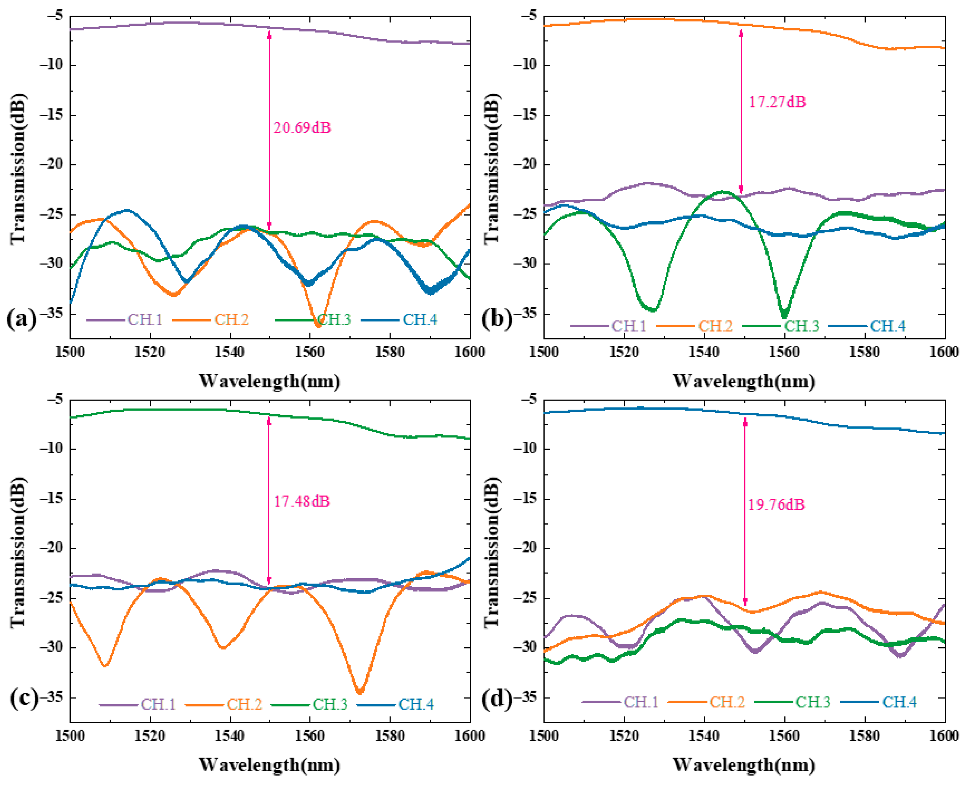
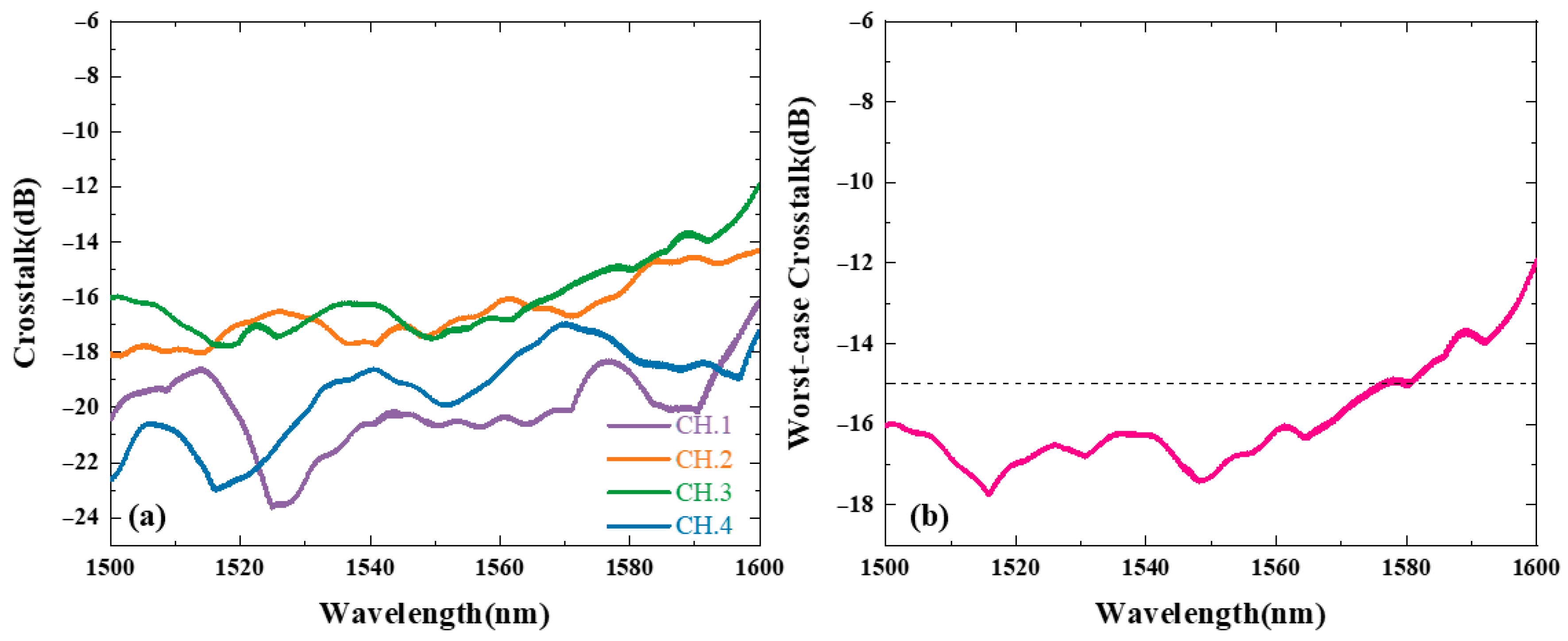
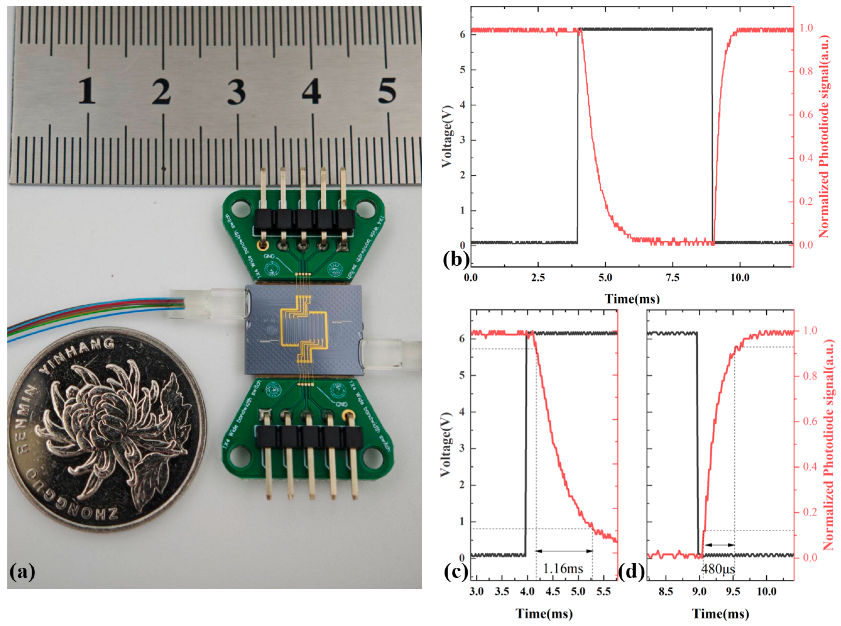
3. Fabrication and Characterizing

The proposed TO switch was fabricated on the silica technology platform (Shijia Ltd., Hebi, China). The fabrication began with the thermal oxidation of a silicon substrate to form a 20 μm thick silica lower-cladding layer. A 4 μm thick germanium-doped silica core layer was then deposited via Plasma-Enhanced Chemical Vapor Deposition (PECVD), with its refractive index tuned through Ge doping concentration. Waveguide patterning was achieved through ultraviolet (UV) lithography and inductively coupled plasma (ICP) etching. A 15 μm thick silica upper cladding layer was subsequently deposited using PECVD, followed by magnetron sputtering of metal electrodes. After dicing, the chip facets were polished at an 8° angle to minimize back-reflection. Finally, a fiber array (FA) coupling assembly and gold wire bonding were implemented for optical and electrical interconnects, respectively.
We built a measurement system to evaluate the fully packaged chip. A tunable laser (TSL−550, Santec., Komaki, Japan) emitted light into a polarization controller, which then passed through the device and entered an optical power meter (MPM−210, Santec., Komaki, Japan). A computer-controlled drive was used to apply a corresponding voltage to the electrodes of the device. The measured spectrum is shown in Figure 4. The insertion loss and power consumption at 1550 nm are listed in Table 2. The measured results show that the device’s output state can be freely switched among the four output ports. The maximum insertion loss (IL) after switching was −6.51 dB, and the crosstalk (XT) values for the four channels were −20.69 dB, −17.27 dB, −17.48 dB, and −19.76 dB, respectively.
Since no additional optical path difference was introduced, resonant effects were suppressed, resulting in an increased operating bandwidth for the device [17]. To demonstrate the device’s bandwidth performance, the crosstalk and worst-case crosstalk spectra are summarized in Figure 5. From Figure 5a, it can be observed that the crosstalk of CH.1 and 4 is better than that of CH.2 and 3. The primary reason is that the symmetry of the 1 × 4 MMI causes similar output characteristics in symmetric channels. Additionally, the simulation data of the 1 × 4 MMI confirm that due to its power-splitting characteristics, CH.2 and 3 exhibit higher insertion loss than CH.1 and 4. The measured results show that the device’s crosstalk becomes worse at wavelengths closer to 1600 nm, which aligns with the simulation results. Nevertheless, as shown in Figure 5b, across the 1500–1580 nm range, the crosstalk remains below −15 dB, covering the entire C-band, and across the 1500–1600 nm range, the crosstalk remains below −12 dB. Due to limitations in the laser’s operational range, the full spectrum could not be completely characterized. We anticipate that the device would also exhibit excellent performance in the S-band.
The device has dimensions of 15.76 mm × 0.86 mm, and a picture of the chip is shown in Figure 6a. Finally, the device’s response speed was measured. A square-wave electrical signal at 100 Hz was applied to the metal heater using an arbitrary waveform generator (SDG6052X, Siglent, Shenzhen, China), and the output signal was transmitted to an oscilloscope (DS4024, RIGOL, Suzhou, China). The rise and fall times of CH.1 in the output 3 state were measured, with the results shown in Figure 6b. The rise time (10–90%) and fall time (90–10%) of the optical signal in the switch were 480 μs and 1.16 ms, respectively, as shown in Figure 6c,d.

4. Discussion

Table 3 lists the research and corresponding data on TO switches in recent years. Ref. [18] designed a 3 × 3 optical switch on a Silicon On Insulator (SOI) platform, where double-spiral modulation arms reduced the phase shifter size while improving the modulation efficiency. However, resonant effects led to bandwidth reduction and deteriorated the crosstalk performance. Ref. [7] proposed a GMZI design implemented on a silicon nitride platform. Benefiting from silicon nitride’s low propagation loss (0.1 dB/cm), the device achieved low insertion loss. Nevertheless, additional optical path differences resulted in large crosstalk. Due to the high refractive index contrast of silicon nitride and SOI devices, their footprint remains small. In contrast, polymer and silica PLCs exhibit smaller refractive index differences, resulting in relatively larger footprints but greater fabrication tolerances. Ref. [17] implemented a logic switch with equal-length modulation arms on a polymer platform. The high TO coefficient of the polymer enabled low power consumption (85.92mW). Through unique structural design, the device achieved crosstalk below −10 dB across all logic states. However, mode mismatch resulted in high coupling losses, leading to an insertion loss of −23.7 dB. Refs. [19,20] demonstrated optical switches fabricated on a silica PLC. Ref. [19] employed a conventional cascaded architecture, while Ref. [20] adopted a GMZI design. Both devices benefited from mature fabrication processes, achieving low insertion losses. The incorporation of air-isolation trenches further reduced power consumption. However, Ref. [19] required complex unit-by-unit calibration during testing, significantly complicating the characterization process. Meanwhile, Ref. [20] exhibited a limited bandwidth of only 2 nm due to the modulation arms.
The silica-based PLC platform, while being a mature commercial solution, suffers from high power consumption due to silica’s low TO coefficient (2.5 × 10⁻⁵/K). Although air isolation trenches and suspended waveguides between modulation arms can reduce power consumption, these structures may increase the device’s response time [21]. During practical measuring, thermoelectric coolers (TECs) are required for device characterization, presenting challenges for completing the packaging process. In this work, the power consumption reached the watt level in the CH.1 output state, which is relatively high for silica TO devices. The measured rise time was on the millisecond scale, primarily attributed to silica’s low thermal conductivity (1.4 W/m·K). Optimizing the upper-cladding thickness could potentially reduce both the switching response time and power consumption. It should be noted that the device’s elevated IL originates primarily from high edge-coupling loss (reference waveguide IL: −5.46 dB). Like all switching devices, this design requires state calibration. However, multi-port switch calibration proves particularly challenging. Implementing an optical feedback system coupled with specialized computer algorithms could enable efficient and precise state control.

5. Conclusions

In summary, in this study, a novel 1 × 4 thermo-optic switch was proposed and fabricated on a silica platform. The device consists of a GMZI structure composed of a dual MMI, with equal-length modulating arms broadening the device’s bandwidth. The advanced process ensures the device’s stable operating state, with an insertion loss of −6.51 dB, crosstalk of −17.27 dB, and power consumption of 1014.41 mW. The crosstalk is less than −15 dB across the 1500–1580 nm range. Limited by the laser’s operating range, the device’s complete performance was not characterized. We speculate that the device will also have excellent parameters in the S-band. As a bandwidth-enhanced GMZI for optical switches, this design demonstrates potential for all-platform implementation.

Funding

This research received no external funding.

Institutional Review Board Statement

Not applicable.

Informed Consent Statement

Not applicable.

Data Availability Statement

The original contributions presented in the study are included in the article; further inquiries can be directed to the corresponding author.

Acknowledgments

Thanks to G. Zeng and X. Wang of Jilin University for their support in the device’s design, and thanks to researcher Y. Wu of the Institute of Semiconductors of the Chinese Academy of Sciences and Shijia Company for their assistance in the device’s fabrication.

Conflicts of Interest

The author declares no conflicts of interest.

References

  1. Masrom, M.; Krisnan, L.; Yahya, Y.; Kaundan, M.K. Patient Attitude on the Application of Artificial Intelligence in Diabetes Care. In Proceedings of the 2024 5th International Conference on Artificial Intelligence and Data Sciences (AiDAS), Bangkok, Thailand, 3–4 September 2024; pp. 441–445. [Google Scholar]
  2. Yoo, S.B. Prospects and challenges of photonic switching in data centers and computing systems. J. Light. Technol. 2021, 40, 2214–2243. [Google Scholar] [CrossRef]
  3. Zeng, Z.; Du, Y.; Qian, Y.; Liu, M.; Chen, C. Index modulation multiple access-aided multi-user VLC for Internet of Medical Things. Opt. Express 2024, 32, 44478. [Google Scholar] [CrossRef]
  4. Sasikala, V.; Chitra, K. All optical switching and associated technologies: A review. J. Opt. 2018, 47, 307–317. [Google Scholar] [CrossRef]
  5. Xu, X.; Zhang, D.; Zhang, P.; Tang, B.; Yin, Y. Multilayer Reconfigurable 3D Photonics Integrated Circuits Based on Deposition Method. Laser Photonics Rev. 2025, 19, 2400827. [Google Scholar] [CrossRef]
  6. Tsai, C.; Tsai, J. MEMS optical switches and interconnects. Displays 2015, 37, 33–40. [Google Scholar] [CrossRef]
  7. Kovaios, S.; Tsakyridis, A.; Giamougiannis, G.; Fotiadis, K.; Sacchetto, D.; Zervas, M.; Moralis-Pegios, M.; Pleros, N. Generalized Mach Zehnder Interferometers Integrated on Si3N4 Waveguide Platform. IEEE J. Sel. Top. Quantum Electron. 2023, 29, 1–9. [Google Scholar] [CrossRef]
  8. Xie, Z.; Bo, F.; Lin, J.; Hu, H.; Cai, X.; Tian, X.-H.; Fang, Z.; Chen, J.; Wang, M.; Chen, F.; et al. Recent development in integrated Lithium niobate photonics. Adv. Phys. X 2024, 9, 2322739. [Google Scholar] [CrossRef]
  9. Zhang, S.; Yin, Y.; Wang, Z.; Li, Y.; Zhang, Y.; Yao, M.; Zhang, D.; Li, Y. Low-Power-Consumption and Broadband 16-Channel Variable Optical Attenuator Array Based on Polymer/Silica Hybrid Waveguide. Photonics 2024, 11, 547. [Google Scholar] [CrossRef]
  10. Ding, Y.; Zhang, D.; Zhang, P.; Tang, B.; Wang, F.; Wang, X.; Yokoyama, S.; Yin, Y. Dual-mode 2 × 2 electro-optic switch on a SOI platform. Opt. Lett. 2024, 49, 6125. [Google Scholar] [CrossRef] [PubMed]
  11. Zhang, Y.; Yin, Y.; Ding, Y.; Zhang, S.; Sun, X.; Zhang, D.; Li, Y. On-Chip E00–E20 Mode Converter Based on Multi-Mode Interferometer. Micromachines 2023, 14, 1073. [Google Scholar] [CrossRef] [PubMed]
  12. Seok, T.J.; Kwon, K.; Henriksson, J.; Luo, J.; Wu, M.C. Wafer-scale silicon photonic switches beyond die size limit. Optica 2019, 6, 490. [Google Scholar] [CrossRef]
  13. Lee, B.G.; Rylyakov, A.V.; Green, W.M.J.; Assefa, S.; Baks, C.W.; Rimolo-Donadio, R.; Kuchta, D.M.; Khater, M.H.; Barwicz, T.; Reinholm, C.; et al. Monolithic Silicon Integration of Scaled Photonic Switch Fabrics, CMOS Logic, and Device Driver Circuits. J. Light. Technol. 2014, 32, 743–751. [Google Scholar] [CrossRef]
  14. Dupuis, N.; Lee, B.G.; Rylyakov, A.V.; Kuchta, D.M.; Baks, C.W.; Orcutt, J.S.; Gill, D.M.; Green, W.M.J.; Schow, C.L. Modeling and Characterization of a Nonblocking 4 × 4 Mach–Zehnder Silicon Photonic Switch Fabric. J. Light. Technol. 2015, 33, 4329–4337. [Google Scholar] [CrossRef]
  15. Pan, S.; Yao, J. UWB-Over-Fiber Communications: Modulation and Transmission. J. Light. Technol. 2010, 28, 2445–2455. [Google Scholar] [CrossRef]
  16. Wei, J.; He, Y.; Yang, Y.; Ding, J.; Lu, L.; Zhu, L. Lightweight optical neural network based on micro-ring resonator. Opt. Express 2025, 33, 10674. [Google Scholar] [CrossRef]
  17. Zeng, G.; Zhang, D.; Wang, F.; Wang, X.; Yin, Y. 1 × N All-Logic Optical Switch Based on Polymer Platform Using Multimode Interferometer. Adv. Photonics Res. 2024, 6, 2400118. [Google Scholar] [CrossRef]
  18. Wang, J.; Niu, H.; Cheng, W.; Shi, S.; Chen, Y.; Guo, C.; Zhu, W.; Hu, G.; Cui, Y.; Yun, B. Compact and power-efficient 3 × 3 silicon photonic interferometer thermo-optic switch. Opt. Express 2025, 33, 12475. [Google Scholar] [CrossRef]
  19. Wang, M.; Yue, J.; Yao, Z.; Liu, T.; Sun, X.; Wu, Y.; Zhang, D. Low-power and wide-band 1 × 8 silica waveguide optical switch. Opt. Laser Technol. 2024, 171, 110380. [Google Scholar] [CrossRef]
  20. Yue, J.; Wang, M.; Zou, J.; Liu, T.; Fang, J.; Sun, X.; Wu, Y.; Zhang, D. Low-loss silica waveguide 1 × 8 thermo-optic switch based on large-scale multimode interference couplers. Opt. Commun. 2024, 573, 131014. [Google Scholar] [CrossRef]
  21. Gao, F.; Xie, W.; Tan, J.Y.S.; Leong, C.; Li, C.; Luo, X.; Lo, G.-Q. Comprehensive Investigation of Thermo-Optic Phase Shifters on a Multi-Layered SiN-on-SOI Platform. J. Light. Technol. 2023, 41, 3108–3114. [Google Scholar] [CrossRef]
Figure 1. Schematic diagram of the GMZI; insert: the cross-section of the waveguide.
Photonics 12 00721 g001
Figure 2. The simulated transmission of (a) CH.1 and (b) CH.2 versus WT1 and WT3; (c) the simulated spectra of the MMI insert with simulated light distribution at 1550 nm.
Photonics 12 00721 g002
Figure 3. Diagram of 1 × 4 switch simulation: (a) CH.1; (b) CH.2; (c) CH.3; (d) CH.4. insert: simulated light distribution.
Photonics 12 00721 g003
Figure 4. The measured spectra of the 1 × 4 switch: (a) CH.1; (b) CH.2; (c) CH.3; (d) CH.4.
Photonics 12 00721 g004
Figure 5. (a) Crosstalk of the 1 × 4 switch. (b) Worst-case crosstalk spectra.
Photonics 12 00721 g005
Figure 6. (a) Diagram of the chip; (b) dynamic response of the switch when a square-wave pulse of 100 Hz is applied to the electrodes; (c) dynamic response of the switch’s fall time; (d) dynamic response of the switch’s rise time.
Photonics 12 00721 g006
Table 1. Summary of parameters.
DimensionW1 × 4 mmiL1 × 4 mmiW4 × 4 mmiL4 × 4 mmiWT1WT2WT3LTW1W2
Value (μm)506355025466.36.28906.4519.39
W: width; L: length; WT: width of taper; LT: length of taper.
Table 2. Measured results of 1 × 4 switch at 1550 nm.
Output StatusPower Consumption
(mW)
IL of CH.1 (dB)IL of CH.2 (dB)IL of CH.3 (dB)IL of CH.4 (dB)
Output10, 317.99, 689.69, 6.73−6.15−26.89−26.85−27.99
Output2471.22, 42.05, 0, 42.05−23.14−5.87−24.16−26.17
Output30, 0, 417.22, 0−24.06−24.11−6.51−23.99
Output40, 623.25, 168.19, 0−29.48−26.18−27.85−6.42
Table 3. Reported data on thermal optical switches.
Ref.PortPlatformIL (dB)XT (dB)Power (mW)Footprint (mm2)Speed (ms)Bandwidth (nm)
[18]3 × 3SOI−3.3−134.60.4/30
[7]4 × 4SI3N4<−3<−83702 × 1.35<10/
[17]1 × 4Polymer−23.7−1085.928.7 × 5.210.38/0.3635
[19]1 × 8Silica−3.4<−15.7315.8 a25.85 × 1.750.94/1.04120
[20]1 × 8Silica−3.69−16.291830 a18.67 × 1.751.0/1.242
This work1 × 4Silica−6.51−17.271014.4115.76 × 0.860.48/1.16100
IL: insertion loss; XT: crosstalk; a average power consumption.
Disclaimer/Publisher’s Note: The statements, opinions and data contained in all publications are solely those of the individual author(s) and contributor(s) and not of MDPI and/or the editor(s). MDPI and/or the editor(s) disclaim responsibility for any injury to people or property resulting from any ideas, methods, instructions or products referred to in the content.

