Review

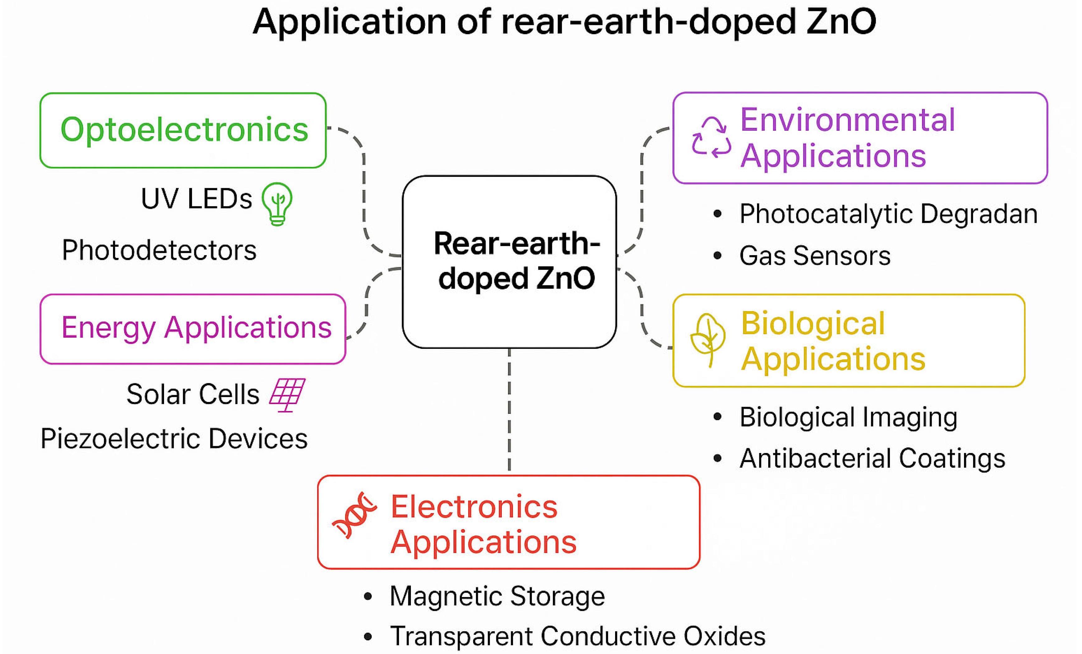
Enhancing Optoelectronic Performance Through Rare-Earth-Doped ZnO: Insights and Applications

1
Department of Physics, University Institute of Sciences, Chandigarh University, Mohali 140413, India
2
Mechatronics Engineering Department, School of Engineering, Manipal University Jaipur, Jaipur 303007, India
3
Regional Institute of Education, National Council of Educational Research and Training (NCERT), Ajmer 305004, India
4
Research and Innovation Cell, Rayat Bahra University, Mohali 140301, India
5
Department of Electrical and Electronics and Communication Engineering, DIT University, Dehradun 248009, India
*
Authors to whom correspondence should be addressed.
Photonics 2025, 12(5), 454; https://doi.org/10.3390/photonics12050454
Submission received: 4 March 2025 / Revised: 27 April 2025 / Accepted: 29 April 2025 / Published: 8 May 2025

Abstract

:
Rare-earth (RE) doping has been found to be a potent method to improve the structural, optical, electronic, and magnetic properties of ZnO, positioning it as a versatile material for future optoelectronic devices. This review herein thoroughly discusses the latest developments in RE-doped ZnO based on the role of the dopant type, concentration, synthesis method, and consequences of property modifications. The 4f electronic states of rare-earth elements create strong visible emissions, control charge carriers, and design defects. These structural changes lead to tunable bandgap energies and increased light absorption. Also, RE doping considerably enhances ZnO’s performance in electronic devices, like UV photodetectors, LEDs, TCOs, and gas sensors. Though, challenges like solubility constraints and lattice distortions at higher doping concentrations are still key challenges. Co-doping methodologies and new synthesis techniques to further optimize the incorporation of RE into ZnO matrices are also reviewed in this article. By showing a systematic comparison of different RE-doped ZnO systems, this paper sheds light on their future optoelectronic applications. The results are useful for the design of advanced ZnO-based materials with customized functionalities, which will lead to enhanced device efficiency and new photonic applications.

1. Introduction

Optoelectronic devices propel technical advancement in the present world, offering applications in energy harvesting, sensing, and communication. Among all semiconductor materials ZnO, TiO2, and SnO have been widely researched for various device applications due to their unique features. Of these materials, ZnO has proved to be a potential candidate with great optical, electrical, and magnetic properties [1,2]. Under ambient conditions, ZnO is characterized by a broad direct bandgap of 3.37 eV with a high transparency across the visible region [3]. Also, ZnO allows an efficient UV light transmission while offering excellent detection capabilities, making it an ideal material for optoelectronic device fabrication [4]. Its high exciton binding energy of 60 meV allows for an efficient light emission at room temperature, further improving its suitability for photonic applications. ZnO plays a crucial role in device engineering, specifically in high-efficiency LEDs, UV-sensitive photodetectors, and laser diodes for optical communication [5]. But ZnO suffers from a decreased visible light absorption and poor electrical conductivity. New studies have applied rare-earth doping to tailor the optoelectronic properties of ZnO so that bandgap engineering, a better carrier mobility, and an improved device performance are achieved [6].
Rare-earth element doping is an effective approach to modify and increase the primary properties of ZnO [7]. The unique electronic arrangements of rare-earth elements, such as Ytterbium, Lanthanum, Terbium, Erbium, and Europium, and elements with partially filled f-orbitals initiate intense and sharp emission lines in the visible light region [8,9]. When rare-earth ions are incorporated into the ZnO crystal lattice, they can increase magnetic properties, improve the visible light emission, and modify the charge carrier concentration, thereby making ZnO suitable for advanced optoelectronic applications [10]. Moreover, rare-earth ions introduce localized states within the ZnO bandgap, enabling bandgap tuning for customized optical and electronic applications [11]. The doping process usually involves replacing Zn atoms in the crystal lattice with rare-earth ions, which impacts electronic band structures and defect states. A key effect is the establishment of recombination centers, leading to new energy bands within the ZnO bandgap and substantially enhancing the light emission properties [12]. For example, Europium (Eu)-doped ZnO has been shown to introduce new energy levels that increase the UV sensitivity in photodetectors, making it a favorable material for future sensing applications [13]. In addition, rare-earth doping supports oxygen vacancy formation, which produces free carriers, thereby improving ZnO’s electrical conductivity and optical performance for transparent conductive oxide (TCO) applications [14].
Recent synthesis advancements allow for the precise control over doping concentrations and nanoparticle morphologies. This enables the fine-tuning of ZnO properties while minimizing secondary phase formation [6]. Such defect engineering under controlled conditions maximizes the luminescence efficiency and charge carrier dynamics, guaranteeing an enhanced device performance. These advancements represent a critical breakthrough in the science of rare-earth-doped ZnO nanomaterials, paving the way for new avenues for high-performance optoelectronic devices. The fabrication of high-quality rare-earth-doped Zinc Oxide nanoparticles (ZnO NPs) is based on three traditional methods: sol–gel processing, hydrothermal synthesis, and Chemical Vapor Deposition (CVD) [15]. These methods allow for precise control over material properties, permitting the development of ZnO-based devices with enhanced performances [16]. However, despite these advancements, challenges continue, particularly at high rare-earth doping concentrations, where aggregation and structural deformations in the ZnO lattice become significant issues [17,18,19]. The low solubility of rare-earth ions in the ZnO matrix tends to cause secondary phase formation, which causes non-uniform doping, a decreased charge carrier mobility, and a degraded optical performance, which impairs ZnO’s optoelectronic efficiency. Scientists have probed co-doping techniques to overcome these constraints, introducing more than one rare-earth element into the ZnO lattice with the aim of enhancing the dopant distribution and minimizing lattice strain. It optimizes the structural integrity while enhancing the electrical and optical characteristics to create improved charge carrier dynamics, increased luminescence, and controlled magnetic behavior. Co-doping enhances the functional diversity of ZnO, positioning it as a strong contender for next-generation optoelectronic applications.
Remarkable advancements have shown the effectiveness of rare-earth-doped ZnO in photonic and sensing applications. For example, Europium (Eu)-doped ZnO shows an enhanced UV sensitivity, making it an exceptional material for high-performance photodetectors [20]. Similarly, Terbium (Tb) doping has allowed for the development of efficient green-emitting LEDs, leveraging its strong luminescence properties [21]. Prior to optoelectronics, rare-earth-doped ZnO has gained interest in catalysis, energy storage, and biomedical applications. The combination of Gadolinium (Gd) and Dysprosium (Dy) induces long-range ferromagnetic ordering, positioning ZnO as a viable candidate for spintronics, quantum computing, and high-density magnetic storage devices [12,22]. In addition, the medical field has examined rare-earth-doped ZnO for bioimaging and medical diagnostics, using its luminescent contrast properties for advanced imaging techniques [9]. Although significant progress has been made, further studies are essential to unravel the mechanisms governing dopant-induced defect states, charge carrier recombination, and band structure modulation. Focusing these elemental aspects will be crucial for realizing the full potential of rare-earth-doped ZnO in future technological and industrial applications [18,19].
To address the challenges of rare-earth doping in ZnO, one needs to overcome solubility limitations and structural deformations at high doping levels. Defeating these challenges calls for advances in synthesis methods and a better understanding of rare-earth doping mechanisms, both of which are important for achieving the full potential of rare-earth-doped ZnO. The prospects of these materials transcend optoelectronics to catalysis, energy storage, and multifunctional nanomaterials [23]. The union of rare-earth elements with ZnO leads to the formation of state-of-the-art functional materials because they have complementary electronic properties and adjustable characteristics. A major scientific challenge is the high doping concentration without negotiating ZnO’s structural integrity. Recent research aims at optimizing synthesis and characterization methods to maximize doping levels without losing ZnO’s functionality. Overcoming these challenges will accelerate the successful integration of rare-earth-doped ZnO into future-generation technologies. Further research in this area will enhance the knowledge concerning dopant–host interactions, particularly the effect of such interactions on altering electronic structures, defect creation, and mechanisms of charge transport—essential determinants for driving future industrial applications.
The function of rare-earth doping in ZnO and how it affects host material properties are the main topics of this review. The incorporation of rare-earth ions into ZnO materials results in significant modifications of its electrical and optical qualities, which produce bright emissions using minimal ion concentrations. It has been observed that the diamagnetic and ferromagnetic properties emerge in rare-earth ions due to their half-filled f-orbitals, making them suitable for magneto-optical device applications. However, at higher doping levels, rare-earth metals can induce structural distortions in ZnO’s hexagonal close-packed structure, changing the optical and electrical properties of the material. This review presents a comprehensive analysis of the changes in ZnO’s structural, optical, and electronic characteristics caused by rare-earth doping, as well as the ramifications for optoelectronic applications. The device structures, operation mechanisms, and doping phenomena will be addressed within the context of some optoelectronic applications, such as solar cells, UV detectors, and sensors. Based on the understanding of the impact of rare-earth incorporation, this review intends to assist in the formation of high-performance ZnO-based materials for future technology development.

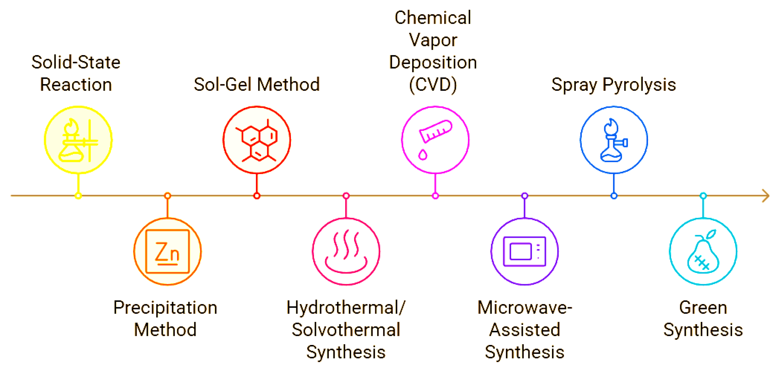
2. Common Methods of Fabrication

2.1. Synthesis Methods Used for ZnO and Doped ZnO Nanostructure

Several synthesis methods are used to generate ZnO nanostructures, and these include co-precipitation, the sol–gel process, and the hydrothermal process. The ZnO and doped ZnO nanostructures for various applications are mentioned in Table 1. Each process provides unique advantages and disadvantages, and these depend on the precursors employed and the preparation conditions. The advantages of co-precipitation methods include an easy and low-cost synthesis route, low-temperature reaction, scalability for large-scale production, control of doping concentration, short reaction time, and small crystallite size in the nanoscale. It has been observed that samples prepared by the co-precipitation method lack uniformity in their crystallite size and morphology. In addition, the agglomeration of particles is common, and pH control is critical for the process’s reproducibility. The use of sol–gel synthesis allows for the easy tuning of the chemical composition and control over homogeneity. The sol–gel method can be used to prepare uniform and doped ZnO thin films and nanoparticles by low-temperature processing. The disadvantages of sol–gel processing include the long processing time, limited scalability, and cracking during the drying/sintering process. The hydrothermal method is well known for the synthesis of complex morphologies, like nanorods, nanowires, nanoflowers, nanorings, etc. This method provides good control over the particle size, shape, and crystallinity. The hydrothermal method can be used to produce single crystals and oriented nanostructures. Some drawbacks of hydrothermal synthesis include a longer reaction time, limited scalability, and limited control during the reaction. In addition, this method requires specialized autoclave equipment with a controlled temperature and pressure. The selection of the synthesis method is critical in dictating the shape, crystalline nature, and functional properties of ZnO NPs. An overview of the representative synthesis methods and their features is shown in Figure 1.
Figure 1. Schematic representation of synthesis routes for ZnO and doped ZnO, highlighting sol–gel, hydrothermal, and CVD techniques.
Photonics 12 00454 g001
Table 1. ZnO and doped ZnO nanostructure for various applications.
S. No.Composition
(ZnO)
MorphologyChange in PropertyApplicationsRef.
1Mn-dopedNanoparticlesChange in optical property by introducing the defects made by Mn dopingSpintronics
Optoelectronics
Photocatalysis
[24]
2Co-dopedNanoparticles
resemble a seed-like structure
Observed the blue shift in the absorbance spectrum with increasing Co doping conc.Photocatalysis
Optoelectronics
Antibacterial activity
[25]
3Cu-dopedNanorodsEnhance the gas sensing response of ZnO nanorodsGas Sensing[26]
4Fe-dopedNanoparticles with euhedral shape and nanowiresViolet emission band at 412 nm (3.0 eV)
Blue emission bands at 468 nm (2.65 V) and 440 nm (2.82 eV)
Photocatalysis
Sensors
Magnetic and Spintronic
[27]
5Zr-dopedNanoparticlesShift in the diffraction peaks to lower angles.
Lattice parameter increases with Zr doping.
Photocatalysis
Antibacterial
[28]
6Eu-dopedNanowirePL studies reveal red emission from the ZnO: Eu.
Sharp emission peak at 612 nm.
LED
Optical Devices
[29]
7Dy-dopedNanoparticlesComplete photodegradation of DR-31 dye.
Maximum sensitivity observed at 150 °C temp.
Photocatalysis
Gas Sensing
[30]
8Tb-dopedThin filmsExhibit strong green luminescence in the spectral region (~1.9–2.6 eV).
Photosensitivity decreases with increasing annealing temperature.
Photodetectors
Thin-film Technologies
[31]
9Ho-dopedNanoflowersShow higher photocatalytic properties.Photocatalytic
UV light sensors
[32]
10Ni-dopedNanoparticlesDRS analysis shows a blue shift in the absorption edge.LED
Spintronic
Gas Sensing
[33]
11Cr-dopedNanowiresAdditional broad absorption tail in the visible region.Photocatalysis[34]
12Ru-dopedNanorodsRTFM is observed in 2 percent of Ru-doped ZnO.Spintronic
Sensors
Catalysis
[35,36]
13Nb-dopedNanorodsOptical transmittance measured in wavelength of 350–1000 nm.Transparent Conducting Oxide
Sensing Device
[36]
14Hf-dopedNanowiresDiffuse reflectance spectroscopy.Photocatalysis
Antimicrobial
[37]
15Hg-dopedNanorodsBand shift towards visible region.Photocatalysis
Optoelectronic
[38]

2.2. Sol–Gel

The sol–gel process is one of the most common methods used for the synthesis of ZnO nanostructures because it is easy, inexpensive, and can be used to tailor the particle size and morphology. The synthesis procedure of rare-earth-doped ZnO nanostructures starts with the measurement of Zinc Acetate Dihydrate (Zn(CH3COO)2·2H2O) and Sodium Hydroxide (NaOH) on a weighing machine. The stoichiometric amount of zinc acetate dissolved in 100 mL of propanol. The magnetic stirrer will be maintained at room temperature and 1200 rpm for 2 h. The stoichiometric amount of rare earth can be added as per the doping concentration. The stirring should continue for 1 more hour until the complete dissolution of the precursor. The appropriate amount of urea [equal to precursor] can be added in the solution to obtain a clear and transparent gel. The temperature should rise to 80 °C to dry the sol. The prepared gel can burn at 500 °C for 30 min followed by calcination at 600 °C. The obtained particles will be rare-earth-doped ZnO nanoparticles.

2.3. Co-Precipitation

The co-precipitation process is a commonly used method for the synthesis of ZnO nanoparticles because it is simple, inexpensive, and can yield high-purity nanostructures at relatively low temperatures. The process is based on the precipitation of ZnO from an aqueous solution by controlled chemical reactions. To prepare ZnO nanoparticles by coprecipitation, 12 g of zinc nitrate hexahydrate (Zn(NO3)2·6H2O) is first dissolved in 100 mL of distilled water with the help of magnetic stirring at a temperature of 50 °C for a time period of 25 min (Equation (1)). Parallelly, 3.2 g of Sodium Hydroxide (NaOH) is dissolved with stirring in 30 mL of distilled water at a temperature of 30 °C for 10 min. Rare earth in stoichiometric amounts should be added to the solution as per the desired doping concentration.
Zn(NO3)2·6H2O(s) → Zn2+(aq) + 2NO3(aq) + 6H2O
The Sodium Hydroxide solution is slowly added dropwise into the zinc nitrate solution under continuous stirring at 50 °C for 3 h. This gradual addition avoids abrupt precipitation and guarantees homogeneous nanoparticle formation. The solution obtained is left to settle for 2 h and then filtered using Whatman filter paper No. 42. In this process, zinc hydroxide precipitates, as illustrated in Equation (2).
Zn2+(aq) + 2OH(aq) + xH2O → Zn(OH)2·xH2O(s)↓
The obtained Zn(OH)2 precipitate is then dried in an oven at 160 °C for 3 h to remove the residual moisture. This is followed by calcination at 300 °C in a furnace, which facilitates the thermal decomposition of Zn(OH)2 into ZnO, as depicted in Equations (3) and (4).
Zn(OH)2·xH2O(s)↓ → Zn(OH)2(s) + xH2O(g)
Zn(OH)2(s) → ZnO(s) + H2O(g)
Finally, the ZnO powder is ground using a mortar and pestle to achieve a uniform particle size and enhance the surface reactivity [39].

2.4. Chemical Vapor Deposition (CVD)

Chemical Vapor Deposition (CVD) is a common method of synthesizing high-quality ZnO thin films with a controlled thickness, composition, and crystalline structures. CVD is widely used in semiconductor and optoelectronic devices, such as thin-film transistors, gas sensors, and transparent conductive oxides. The process of CVD for ZnO thin film deposition involves several steps that facilitate uniform growth and optimal material properties, as shown in Figure 2.
The Chemical Vapor Deposition (CVD) enables controlled doping and the uniform particle growth of rare-earth-doped ZnO nanoparticles. Zinc precursors (zinc acetate, zinc nitrate, and diethyl zinc) are evaporated with a rare earth precursor selection between rare earth nitrate and acetylacetonate through the transport of reaction gases by inert or reactive carrier gas streams using argon, nitrogen, or oxygen gases. The process of generating ZnO nanoparticles involves heating zinc precursors at specific temperatures ranging from 400 °C to 700 °C within the reaction chamber. During the termination of the rare earth precursor both dopant ions dissolve either into the ZnO lattice structure or attach themselves to the developing nanoparticles. Following deposition, the nanoparticles recover from the substrate and chamber walls before possible post-synthesis annealing improves their structural along with optical properties.

2.5. Hydrothermal Method

The hydrothermal process is a common method of synthesizing high-quality ZnO nanostructures, which has advantages including a low processing temperature, high crystallinity, and controlled morphology. The process involves the precipitation of ZnO under high-temperature and pressure conditions within a sealed reaction vessel. The synthesis is initiated with the dissolution of 0.72 g of Sodium Hydroxide (NaOH) and 0.31 g of Zinc Acetate Dihydrate (Zn(CH3COO)2·2H2O) into 40 mL of deionized water with regular stirring. Stirring facilitates the uniform dispersion of precursors and the effective dissolution of reactants. The stochiometric amount of rare earth acetate can be added as per the required doping concentration. After the completion of the dissolution process, the solution is filled into a Teflon-lined stainless-steel autoclave, which allows for a high-pressure environment for ZnO’s crystal growth. The other preparation involves submerging Graphite sheets and graphene substrate separately into the reaction solution, so substrate integration could be possible during ZnO synthesis. Afterwards, the autoclave is sealed and is heated at 70 °C for 20 h to allow for nucleation and the ZnO nanostructures’ growth under controlled hydrothermal conditions. Following the reaction, the white ZnO precipitate is removed and cleaned several times using ethanol and deionized water for any remaining impurities. The final product is conditionally dried under controlled conditions so that it is free from contaminants and structurally stable before proceeding to further application testing and characterization [40]. The hydrothermal process offers a number of benefits, including the ability to control the ZnO nanostructure morphology, high accuracy, environmentally benign processing, and compatibility with different substrates. By varying reaction conditions like the temperature, time, and precursor concentration, scientists can design ZnO’s properties for optoelectronic, sensor, and photocatalytic applications.

3. Discussion of Doped ZnO Properties and Applications

3.1. Transition-Metal-Doped ZnO

Transition-metal-doped ZnO has drawn plenty of attention within the scientific fraternity as a result of its changed intrinsic properties that boost its efficacy in application, such as in photocatalysis, optoelectronics, and spintronics. Nominally, pure ZnO is a wide-bandgap semiconductor having a bandgap energy of 3.37 eV. However, incorporating transition metals, like Iron (Fe), Manganese (Mn), Cobalt (Co), Nickel (Ni), and Copper (Cu), enormously alters their electronic, optical, and magnetic attributes [41]. The incorporation of transition metal dopants brings in extra energy levels within the ZnO bandgap, thus expanding its light absorption ability into the visible region, which is especially beneficial for photocatalysis. The photocatalytic activity of Cu-doped ZnO is significantly improved under visible light because of the presence of Cu⁺ and Cu2+ oxidation states, which allow an efficient electron–hole pair separation and minimize charge recombination losses. In addition to photocatalysis, doping with transition metals results in an extensive alteration of ZnO’s magnetic behavior. Although ZnO is diamagnetic in its pure form, Mn, Co, and Ni incorporation introduces ferromagnetic ordering into ZnO, making ZnO a promising material for spintronics [42]. Mn-doped ZnO exhibits room-temperature ferromagnetism, which is highly desirable for applications in magnetic sensors and memory storage devices [43].
Transition metal doping also influences ZnO’s electrical conductivity, leading to a transformation from n-type to p-type conductivity, which is critical for the fabrication of p–n junctions used in diodes and transistors [44]. Additionally, transition metal dopants enhance the crystalline quality and surface properties of ZnO, thereby improving its gas sensing capabilities [45]. These improvements render transition-metal-doped ZnO very appropriate for gas sensor applications, as well as for its applications in environmental photocatalysis, magnetic sensing, and optoelectronic devices. The selection of the transition metal dopant is determined by the intended application, since each dopant individually influences ZnO’s physical and chemical characteristics. Knowledge of these alterations is important for optimizing ZnO-based materials to address particular functional demands in next-generation electronic and photonic technologies [46].

3.2. Rare-Earth-Doped ZnO

The addition of rare-earth ions, like Cerium (Ce), Europium (Eu), Terbium (Tb), Erbium (Er), and Neodymium (Nd), into the ZnO lattice increases its optical, electrical, and photocatalytic behaviors to a great extent. The insertion of rare-earth ions provides extra energy levels inside the bandgap of ZnO and, thus, increases light absorption and emission properties. Therefore, Europium (Eu)- and Terbium (Tb)-doped ZnO show a strong luminescence and, thus, are very well suited for use in phosphors, light-emitting diodes (LEDs), and display technologies. Likewise, regarding visible light luminescence, Erbium (Er) doping in ZnO allows for infrared emission, which is critical for optical communication and laser technology. These increased luminescent properties are the basis for high-performance optoelectronic devices. In addition to optical improvement, rare-earth doping also enhances ZnO’s photodynamic and magnetic characteristics, rendering it a highly versatile material. Rare-earth doping enhances the photocatalytic efficiency of ZnO, allowing it to achieve a high efficiency under both UV and visible light exposure. It was also observed that the Ce-doped ZnO has an enhanced efficiency in pollutant degradation by creating intermediate energy levels, which enable an efficient electron–hole pair separation and suppress recombination losses [47]. Also, rare-earth-doped ZnO exhibits magnetic behavior, making it potential material for spintronic applications and magnetic sensors. Specifically, Neodymium (Nd) and Samarium (Sm) doping induces ferromagnetic properties, broadening ZnO’s application scope [48]. The altered characteristics of rare-earth-doped ZnO render it most appropriate for futuristic technological applications, such as solar cells, magnetic sensors, photocatalysis, and luminescent devices. The possibility of controlling optical, electronic, and magnetic properties with the help of the accurate selection of rare-earth elements and doping concentration guarantees its widespread applicability in future optoelectronic- and energy-related devices [49]. Rare-earth ions have also been reported in the Re2+ oxidation state as a divalent impurity. Julien Petersen et al. reported on an Eu-doped ZnO thin film prepared by sol–gel and magnetron sputtering with the presence of Eu2+ and Eu3+. The presence of Eu2+ may be attributed to the formation of Eu2O3 [50]. Rare-earth metals play a critical role in modulating the optical and electronic properties of advanced optoelectronic devices. Their unique 4f electron configurations give rise to sharp, well-defined emission peaks that are largely unaffected by the surrounding chemical environment, making them ideal for achieving a high color purity and wavelength-specific light emission. Incorporating ions such as Eu3+, Tb3+, or Er3+ allows for precise control over the emission spectrum, enabling the design of devices with enhanced color selectivity and luminance efficiency. The rare-earth ions have characteristic emissions in visible regions due to the f-f transition. Beyond their optical advantages, rare-earth ions can also influence the electronic structure of host materials by introducing localized energy levels that facilitate energy transfer processes or act as recombination centers. This interaction can help improve exciton confinement and reduce non-radiative losses. The apparent bad gap reduction in rare-earth-doped ZnO is due to the formation of a trap level by rare earth dopant ions. Moreover, rare-earth doping affects charge carrier dynamics by altering injection and transport, often promoting a better charge balance and suppressing exciton quenching. These effects contribute to improved device performance, including a higher quantum efficiency, lower driving voltages, and enhanced operational stability. Therefore, the strategic integration of rare-earth elements is essential for optimizing the overall functionality and durability of luminescent and electronic devices.
Rare earth (RE)-doping significantly enhances the functional properties of ZnO-based materials by introducing 4f electron states that interact with ZnO conduction and valence bands, resulting in intermediate energy levels that facilitate photon absorption and promote a more efficient charge carrier excitation. The incorporation of RE ions, due to their large ionic radii and unique electronic configurations, induces a localized lattice strain and generates defect states, particularly oxygen vacancies, which act as shallow donors to enhance the n-type conductivity. These defect sites also serve as charge trapping centers that reduce the electron–hole recombination, thereby improving the carrier lifetime and charge transport dynamics. Furthermore, RE doping can modulate ZnO’s band structure and increase dielectric polarization, leading to an enhanced piezoelectric and optoelectronic response. These synergistic effects make RE-doped ZnO highly suitable for high-performance applications in sensing, LED, solar cell, gas sensing optoelectronics, and UV photodetector applications. The operation of optoelectronic devices depends on the number of charge carriers and the defect concentration. Rare-earth-doped ZnO has shown a change in the electron concentration due to the mismatch in the oxidation state of Zn2+ and RE3+ ions. The XPS analysis ascertains that the defect oxygen concentration can be tuned by the incorporation of suitable rare earth dopants in appropriate concentrations. It has been proven that the incorporation of rare earth not only produces the characteristics of an intense emission, enhanced conductivity, tunable magnetic properties, and the possibility of band gap engineering but also improves the ZnO characteristic properties. Therefore, the device performance can be improved by tuning factors such as the defect concentration, electron concentration, trap level, and localized magnetic moment by doping rare earth in the ZnO nanostructure.

3.3. Sc-Doped ZnO

The Scandium (Sc) doping of ZnO (ZnO: Sc) increases its optical transmittance and electrical conductivity and makes it a valuable material for thin-film applications. In this research, ZnO: Sc thin films were prepared via the sol–gel method and coated on c-plane sapphire substrates. The precursor solution was Zinc Acetate Dihydrate dissolved in 2-methoxyethanol, and the stabilizer used was monoethanolamine. Scandium doping was performed by adding 0.5 wt.% of Scandium Nitrate Hexahydrate to the precursor solution. This work examines the effect of the annealing temperatures from 300 °C to 550 °C on the structural, optical, and electrical properties of ZnO: Sc films [51]. Figure 3a shows that Sc thin films were found to be highly dependent on the annealing temperature. As shown in Figure 3b, the Full Width at Half Maximum (FWHM) values initially decrease as the annealing temperature increases from 300 °C to 400 °C, indicating an improvement in crystallinity due to the grain growth and reduced structural defects. However, beyond 400 °C the FWHM values increase and the XRD peak intensities decline, suggesting a deterioration in crystallinity, potentially due to increased grain boundary defects or secondary phase formation. The crystallite size increases with the rising annealing temperature, which corresponds to a reduction in structural defects, leading to better crystallinity (Figure 3b). The enhancement in the crystallite size and the reduction in micro strains indicates an improvement in the ZnO: Sc film quality with optimized annealing conditions. The shift in diffraction peak positions (2θ) and changes in the lattice constant (c) as a function of the annealing temperature are shown in Figure 3c. The systematic shift in 2θ values with the increasing temperature suggests a strain relaxation within the ZnO lattice, leading to improved structural stability. The variation in the lattice constant (c) further confirms the effect of thermal annealing on the ZnO matrix, indicating a transition toward an energetically favorable crystal structure. These findings emphasize the crucial role of the annealing temperature in determining the structural quality and phase stability of Sc-doped ZnO thin films. Optimizing the thermal treatment process can significantly enhance the crystallinity, lattice stability, and defect reduction, making ZnO: Sc an ideal candidate for transparent conductive electrodes, optoelectronic devices, and sensor applications.
Figure 3. XRD patterns of films annealed at different temperatures (a) and their corresponding variations in FWHM, crystallite size (b), 2θ position, and lattice constant (c). (Reproduced with the permission of ref. [51], Elsevier, 2010).
Photonics 12 00454 g003

3.4. La-Doped ZnO

Lanthanum (La) doping is an established technique to alter the structural, optical, and electrical characteristics of ZnO and is thus very promising for optoelectronics, photocatalysis, and gas sensing. La3+ ion incorporation into the ZnO lattice results in lattice distortion, attributed mainly to the fact that the ionic radius of La3+ (103.2 pm) is larger than that of Zn2+ (74 pm). This replacement results in a crystal strain, grain size diminution, and defect creation, which subsequently alter the bandgap energy, increase the photoluminescence (PL) efficiency, and enhance charge carrier dynamics. Through the creation of new localized energy levels in the ZnO bandgap, La doping successfully increases the light absorption and modifies radiative recombination mechanisms, rendering it a strong contender for next-generation optical and electronic devices. The existence of La-related defect states is pivotal to bandgap modulation, affecting the emission spectra and defect-induced luminescence. The photoluminescence (PL) spectra of pure and La-doped ZnO, as shown in Figure 4 and Figure 5, demonstrates drastic modifications in the emission intensity, peak energy, and broadening of the spectrum, testifying to the influence of La doping on optical and defect emissions. Figure 4 shows the PL intensity (cps) within wavelengths (310–600 nm) for different La concentrations (0.0 wt.% to 7.5 wt.%.) The maximum PL intensity of 561 cps is found at 7.5 wt.% La, indicating an enhanced radiative recombination because of shallow donor-level formation. The prominent peaks found at 438, 451, 468, 482, 493, and 561 nm are related to defect emissions, such as oxygen vacancies (Vₒ), zinc interstitials (Znᵢ), and La3+-created energy levels [1]. The blue shift in the PL peaks with increasing La contents suggests bandgap widening due to enhanced charge carrier confinement.
Figure 4. PL spectra of pristine and La-doped ZnO (reproduced with the permission of ref. [1], Elsevier, 2020).
Photonics 12 00454 g004
Figure 5 shows the PL spectra of LaxZn1−xO nanomaterials, for which x ranges from 0 to 0.07, recorded over a wavelength range of 390–600 nm. The intensity of PL has a direct relationship with the increase in the La concentration, validating the involvement of La in creating defect-related radiative centers that affect optical transitions. The narrow peak at ~420 nm is indicative of a near-band-edge (NBE) excitonic recombination, while broader emissions at longer wavelengths are indicative of deep-level transitions due to defects [19]. The enhanced intensity with increased La doping concentrations indicates a better electron-hole–pair separation, which favors photocatalytic and optoelectronic functions. These findings agree that the La incorporation efficiently modulates ZnO’s luminescence characteristics by adjusting defect concentrations, creating localized states, and promoting excitonic transitions. The capability to adjust the PL intensity and emission peaks by tuning the La concentration makes it a good approach to create high-performance light-emitting devices, UV detectors, and photocatalytic materials.
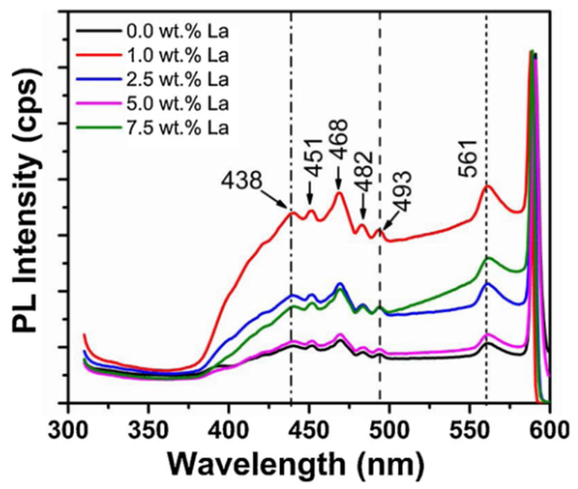
  • Bandgap modulation and quantum confinement effects:
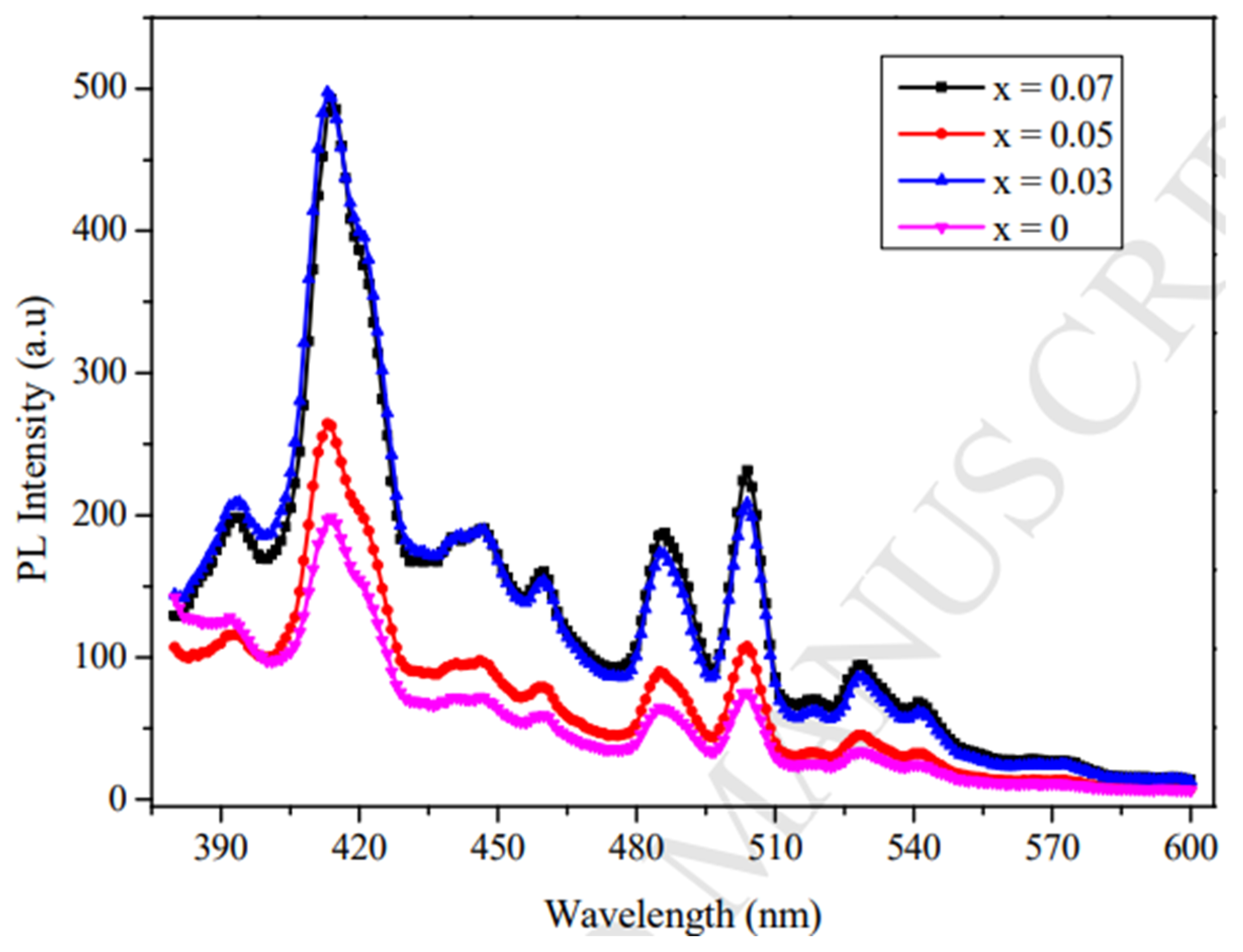
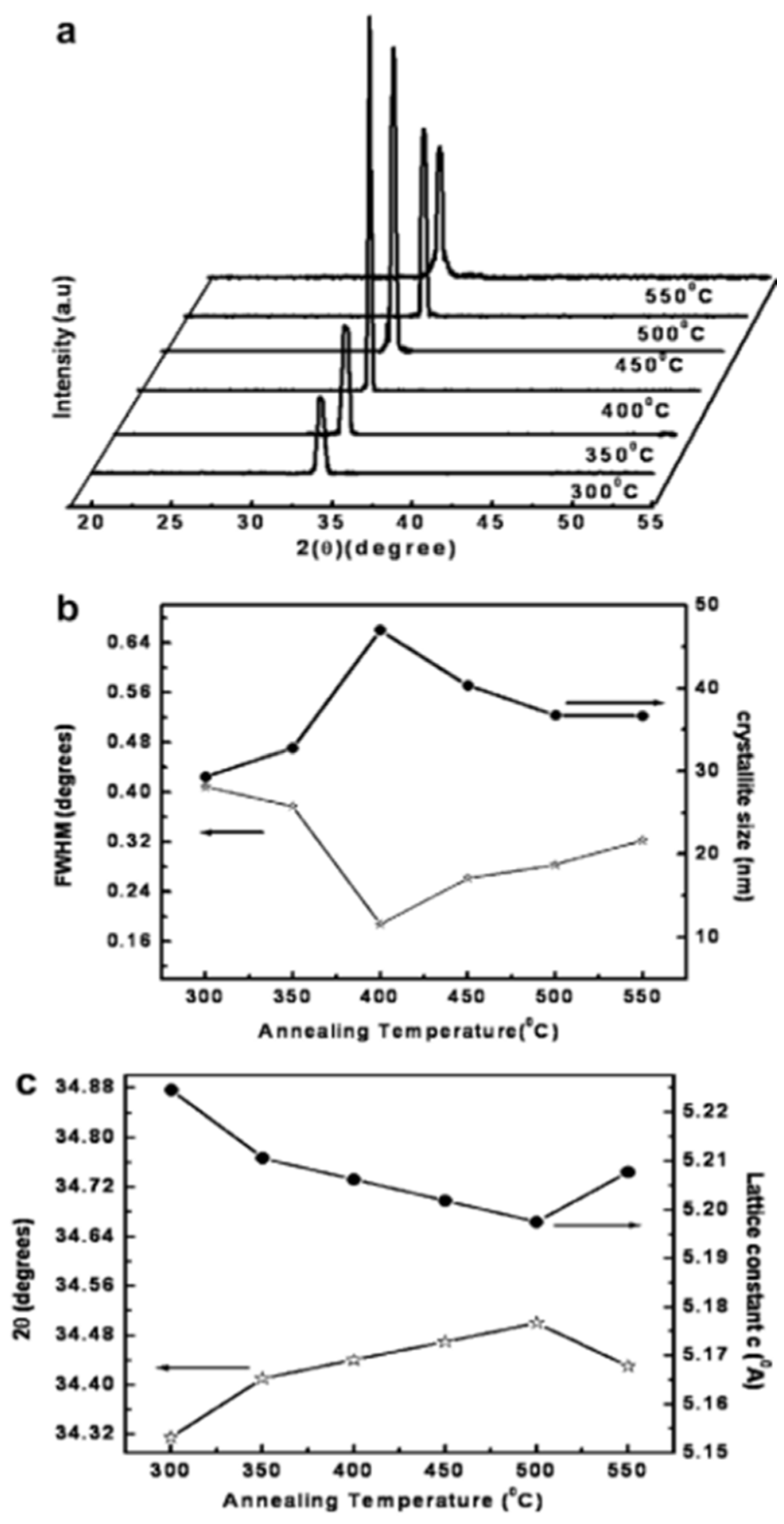
La3+ ion incorporation causes the widening of the bandgap by the creation of localized states in the vicinity of the conduction band, thereby improving the excitonic recombination efficiency. The blue shifting of the emission peaks indicates a decrease in mid-gap states, leading to a more efficient UV-visible emission. La3+ doping also creates oxygen vacancies (Vo) and zinc interstitials (Zni), which alter deep-level emissions (DLEs). The increased electron–hole pair separation caused by La-induced energy levels decreases the non-radiative recombination; hence, the PL intensity increases. The La–O bond formation inhibits non-radiative recombination channels, resulting in an improved quantum efficiency in PL emissions. The increased PL intensity at elevated La levels suggests an enhanced radiative recombination, which is essential for light-emitting and sensing devices.
Figure 5. PL spectra of LaxZn1−xO nanomaterials (reproduced with the permission of ref. [19], Elsevier, 2017).
Photonics 12 00454 g005
Lanthanum doping is a powerful approach for optimizing ZnO’s electronic and optical properties by adding localized defect states, enhancing the charge carrier separation, and modulating the bandgap energy. The large PL enhancement and emission shifts with the introduction of La are indicative of its promising role in light-emitting devices, optoelectronic sensors, and photocatalysts. The optimization of dopant concentration allows for the precise regulation of optical transitions and defect state tailoring, which renders La-doped ZnO an essential material for next-generation optoelectronic technology.

3.5. Dy-Doped ZnO

Dysprosium (Dy)-doped ZnO shows remarkable enhancements in structural, optical, magnetic, and photocatalytic characteristics, representing a versatile material to be used in many technological applications. Dy3+’s larger ionic radius (106 pm) than that of Zn2+ (74 pm) causes lattice changes, which affect the grain size, surface reactivity, and defect generation. These modifications affect the bandgap energy, photoluminescence (PL) emission, and defect concentration, making Dy-doped ZnO an extremely useful material in LEDs, solar cells, gas sensors, and environmental purification.
  • Structural and morphological changes due to Dy doping:
The Scanning Electron Microscope (SEM) images in Figure 6 elucidate the variation in ZnO morphological properties with increasing doping concentrations of Dy (0.25% to 4%). The following key observations can be made. The grain size decreases with the rise in Dy concentrations, suggesting that the Dy3+ incorporation suppresses grain growth by forming Dy–O–Dy bonds. Low Dy concentrations (0.25% to 1%) maintain a well-defined granular structure with a regular particle distribution in ZnO. Increased Dy doping concentrations (2% to 4%) increase the surface roughness, which can be useful for enhancing adsorption characteristics for photocatalysis and gas sensing. Film Thickness and Roughness: the SEM cross-sectional analysis indicates that Dy doping makes the film thickness higher, with values between 200 and 300 nm, verifying that a greater Dy content yields denser and rougher films. The enhanced roughness at greater doping concentrations can enhance the light absorption efficiency in optoelectronic applications. The particle size reduces on average from ~900 nm (undoped ZnO) to ~500 nm at 4% Dy doping, indicating that Dy serves as a growth inhibitor, limiting excessive crystal growth [52]. The formation of Dy–O–Dy bonds impedes grain coalescence, leading to a more dispersed and uniform nanostructure, which is crucial for gas sensing and photocatalytic applications.
Dy doping changes the ZnO bandgap, inducing a blue shift in the optical absorption edge, as confirmed by UV-visible spectroscopy. The increase in the bandgap energy is attributed to quantum confinement effects and the structural disorder introduced due to the Dy incorporation. Dy-doped ZnO can be effectively utilized in UV photodetectors and transparent electronic devices because of an increased bandgap. Photoluminescence (PL) Enhancement: Dy-doped ZnO exhibits an impressive improvement in its PL intensity, confirming the formation of defect states and enhanced charge carrier separation. The presence of Dy3+ energy levels within the ZnO bandgap is responsible for high visible emissions, making it a promising material for LEDs and luminescent coatings. The blue emission observed in Dy-doped ZnO is explained by oxygen vacancy (Vo)-mediated defect states, which are of crucial relevance for phosphor-based applications [53]. Furthermore, pure ZnO exhibits diamagnetic behavior, but Dy doping induces weak ferromagnetism at room temperature. The formation of Dy–O–Zn bonds alter exchange interactions, contributing to long-range magnetic ordering. The observed ferromagnetic behavior in Dy-doped ZnO makes it a suitable candidate for spintronic devices and magnetic storage applications. Magnetic Defects and Exchange Interactions: The increase in the defect concentration (oxygen vacancies and zinc interstitials) enhances the ferromagnetic response in Dy-doped ZnO. The presence of Dy3+ ions disrupts the long-range ordering of ZnO’s wurtzite structure, modifying the spin alignment and contributing to magnetic anisotropy.
Similarly, the Dy-doped ZnO demonstrates enhanced photocatalytic activity under UV and visible light irradiation, making it effective for environmental remediation [54]. The increased surface area, higher defect concentration, and improved charge carrier separation boost the degradation efficiency of organic pollutants, such as methylene blue and rhodamine B. Gas Sensing Capabilities: Dy doping improves ZnO’s sensitivity toward toxic gases, enabling its use in gas detection applications. The rougher surface morphology and defect engineering enhance the material’s adsorption capacity for gas molecules, making it ideal for NO2 and NH3 sensors. Furthermore, the incorporation of Dy3+ ions leads to a reduction in grain size and an increase in film roughness, which enhances the surface reactivity and improves its effectiveness in photocatalysis and gas sensing applications. The optical properties of ZnO are also notably improved, as Dy doping induces an enhanced photoluminescence with strong visible emissions, making it a suitable candidate for LEDs, phosphor-based coatings, and luminescent displays. In addition to its optical enhancements, Dy-doped ZnO exhibits room-temperature ferromagnetism (RTFM) due to the formation of Dy–O–Zn exchange interactions, which introduce magnetic ordering within the ZnO lattice. This magnetic behavior makes Dy-doped ZnO highly applicable for spintronic devices and magnetic storage applications. Furthermore, Dy incorporation enhances the photocatalytic efficiency, allowing for an improved organic pollutant degradation under UV and visible light irradiation, making it a promising material for environmental remediation and wastewater treatment. By optimizing the Dy concentration, ZnO’s functional properties can be tailored to meet the demands of next-generation optoelectronic, spintronic, and energy-related applications. The ability to precisely tune the bandgap energy, defect density, and charge carrier dynamics through Dy doping further solidifies its potential in advanced material engineering for future technological innovations. The rare-earth-doped ZnO for various applications is mentioned in Table 2.
Figure 6. SEM of (i) 0.25 Dy, (ii) 0.50 Dy, (iii) 1.00 Dy, (iv) 2.00 Dy, (v) 3.00 Dy, and (vi) 4.00 Dy. (Reproduced with the permission of ref. [52] Elsevier, 2025).
Photonics 12 00454 g006
Table 2. Rare-earth-doped ZnO for various applications.
Rare EarthSynthesis
Process
PropertiesApplicationsRef.
Scandium (Sc)Sol–Gel
I.
Nano rod formation (SSEM and AFM analysis).
II.
>89% transmittance in the visible region.
III.
Minimum resistivity: 3.52 × 10⁻⁴. Ω∙cm at 0.5 wt.% Sc, 400° annealing.
Transparent electrode for displays and solar cells.
Gas censors, photocatalysis, and field emission devices.
[51]
Lanthanum (La)Chemical Method
I.
Band gap decreases with La doping.
II.
UV-visible and PL spectra confirm band gap narrowing and defect states.
Antibacterial coatings and photocatalysis.[19]
Yttrium (Y)Sol–Gel
I.
(002) preferred orientation.
II.
Y-doped ZnO lacks green emission (pure ZnO: 3.22 eV and 2.38 eV peaks).
Transparent conductive films, sensors, and photodetectors.[55]
Cerium (Ce)Wet Chemical method
I.
Rectifying behavior observed for both pure and Ce-doped ZnO nanoparticles.
II.
Green emission band broadens with Ce3+ doping.
LEDs, display technology, optical sensors, diodes, and electronic switching devices.[56]
Dysprosium (Dy)Co-precipitation method
I.
Increased defect concentration with Dy doping.
II.
Blue shift in band gap with Dy doping.
Defect engineering in optoelectronics, photocatalysis, and UV sensors.[53]
Terbium (Tb)Wet Chemical methodRedshift in UV emission due to defect states and shallow energy levels.Optoelectronics devices, phosphors, and UV sensors.[57]
Samarium (Sm)Solid-state method
I.
Sm ions participate in luminescence.
II.
Enhanced room-temperature ferromagnetism.
III.
Redshift in absorption edge.
White LEDs display technology, spintronic devices, and magnetic sensors.[58]
Neodymium (Nd)Chemical synthesis method
I.
Enhanced ferromagnetism with Nd doping.
II.
Improved photocatalysis compared to pure ZnO.
Spintronics, magnetic storage, environmental remediation, and water purification.[59]
Praseodymium (Pr)Electrospinning method
I.
Enhanced acetic acid sensing at 380 °C.
II.
Pr-doped ZnO shows high selectivity for acetic acid, acetone, and methanal.
Gas sensors for acetic acid, industrial and environmental gas monitoring.[60]
Lutetium (Lu)Sol–Gel method
I.
Conductivity high in vacuum.
II.
Optical transmittance increases with Lu3+ doping.
Transparent conductive films and sensors.[61]
Gadolinium (Gd)Solid-state reaction method
I.
Polycrystalline nature confirmed.
II.
FTIR bands < 800 cm−1 indicate atomic modification,
Optoelectronics devices, sensors, and as a catalyst material.[62]
Thulium (Tm)Spin Coating and hydrothermal
I.
Nanorod shape confirmed via XRD and SEM.
II.
Bandgap found to be 3.35 eV.
Used in transparent conductive films and TCOs.[63]
Ytterbium (Yb)Polymerization–solution method
I.
Crystallite Size < 20 nm.
II.
Hexagonal wurtzite structure retained.
Nanostructured coating and catalyst.[64]
Europium (Eu)Spray pyrolysis method
I.
Eu3+ incorporation creates oxygen vacancies.
II.
Photocatalytic activity.
Enhanced charge separation and environmental remediation.[65]
Erbium (Er)Sol–gel methodHigher dielectric constant.Capacitors and high-frequency electronics.[66]
Samarium (Sm)Sol–gel method
I.
Crystallite size increases with Sm doping.
II.
Effective against E. coli, K. pneumonia, S. aureus.
Biomedical coatings and antibacterial materials.[67]
Holmium (Ho)Combustion method
I.
Ho3+ ions incorporated into ZnO lattice.
II.
Nanoparticles with size decreasing as Ho content increases.
Nanostructured coatings, catalysis, and functional materials for electronics.[68]

3.6. Applications of ZnO

Zinc Oxide (ZnO) is a multifunctional material with diverse applications across industrial, medical, electronic, and environmental domains. Its unique optical, electrical, magnetic, and antimicrobial properties make it an essential component in consumer products, healthcare, advanced electronics, and spintronics. The wide bandgap (3.37 eV) and high exciton binding energy (60 meV) of ZnO enable its use in ultraviolet (UV) light-emitting diodes (LEDs), photodetectors, and transparent conductive films. Additionally, ZnO’s nanostructured forms, including nanoparticles, nanorods, and thin films, enhance its performance in antimicrobial coatings, catalysis, and gas sensing. The ability to engineer ZnO’s properties through doping and nanostructuring further expands its usability in next-generation electronic, spintronic, and biomedical technologies.

3.6.1. Application of ZnO in Optoelectronics

The combination of a wide bandgap (3.37 eV) and strong exciton binding energy (60 meV) makes ZnO highly suitable for optoelectronic applications, such as UV photodetectors, LEDs, and solar cells. UV-sensitive ZnO photodetectors offer high detection efficiency and fast response times, making them ideal for environmental monitoring and biomedical imaging. Rare-earth doping enhances the charge carrier mobility and extends the spectral response duration, further improving the performance of ZnO-based devices. The emission efficiency of ZnO light-emitting devices is also enhanced through doping, while the defect resistance increases, enabling applications in displays and light-emitting devices operating in the UV and visible regions. ZnO also serves as a TCO in thin-film solar cells, playing a dual role in light absorption and charge transport. Doped ZnO photovoltaics achieve higher power conversion efficiency and better charge separation, improving the overall solar cell performance. Additionally, the small-scale architecture of ZnO nanorods and nanowires enables the fabrication of flexible optoelectronic devices, enhancing the sensor capabilities, laser diode performance, and photonic device efficiency. The applications of ZnO in different areas are shown in Figure 7. This review confirms ZnO’s role as a critical material for next-generation optoelectronic systems, with potential applications in high-performance sensing, energy conversion, and light-emitting technologies.

3.6.2. Doped ZnO in Solar Cells

Solar cells, also known as photovoltaic (PV) cells, generate electricity through the photoelectric effect, where semiconductor materials absorb sunlight and create electron–hole pairs. In traditional silicon-based solar cells, incident photons excite electrons, allowing them to migrate toward the n-type semiconductor, while holes move toward the p-type region under the influence of a built-in p–n junction electric field. The separation of charge carriers enables the flow of the current when the cell is connected to an external circuit. The overall efficiency of a solar cell depends on three key factors: photon absorption efficiency, charge separation effectiveness, and charge carrier transport quality. ZnO plays a crucial role in enhancing solar cell performance, primarily as a TCO layer in thin-film and perovskite solar cells. It serves as a highly transparent window layer, allowing maximum light penetration while simultaneously conducting electricity. ZnO is increasingly preferred over Indium Tin Oxide (ITO) due to its lower cost, environmental abundance, and comparable optical and electrical properties.
  • Role of doped ZnO in solar cells:
In perovskite and thin-film solar cells, doped ZnO is widely used as an electron transport layer (ETL) to facilitate efficient electron collection and charge separation while minimizing recombination losses, leading to a higher energy conversion efficiency [69]. Anti-Reflective and Light-Scattering Properties: ZnO exhibits photocatalytic functions and acts as an anti-reflective coating, reducing light reflection and increasing light absorption. Its scattering properties improve light trapping by extending the optical path length, which is particularly beneficial for thin-film and nanostructured solar cells. Passivation Layer for Surface Defect Reduction: ZnO contributes to passivating surface defects, which reduces the trap states and charge recombination, improving the overall stability and longevity of solar devices. Rare-earth-doped Zinc Oxide (ZnO) has demonstrated significant promise in the performance improvement of solar cells, especially in their efficiency, stability, and light absorption characteristics. ZnO, being a wide-bandgap semiconductor, is widely employed in different layers of solar cells, like the electron transport layer, because of its superior electrical properties, stability, and transparency. But doping ZnO with rare-earth elements, such as Europium (Eu), Terbium (Tb), or Dysprosium (Dy), enhances its optical and electrical properties, which are essential for maximizing the solar cell performance. The incorporation of rare-earth dopants into the ZnO matrix has been shown to increase light absorption by changing the electronic structure and introducing supplementary energy levels inside the bandgap. This enables an improved harvesting of solar energy, particularly in the ultraviolet (UV) and visible ranges, by enhancing the material’s light absorption capability over a broader spectrum. The dopants also enhance the charge carrier dynamics, minimizing recombination losses and enhancing the overall efficiency of the solar cell by enabling faster electron transport. In addition, rare-earth-doped ZnO enhances the durability and stability of solar cells, enhancing their resistance to environmental conditions like humidity and temperature. This plays a crucial role in boosting the long-term performance and longevity of solar panels, which is important for commercial as well as domestic use. In addition, rare-earth dopants facilitate the reduction in the material’s vulnerability to defects, which might otherwise compromise solar cell efficiency in the long term. For thin-film and dye-sensitized solar cells, rare-earth-doped ZnO has been studied for its application as a photoanode, where it can enhance the electron injection efficiency and increase the overall power conversion efficiency. As this research continues to advance, rare-earth-doped ZnO promises to be an integral part of developing more efficient, less expensive, and long-lasting solar energy technologies.
  • Performance and stability:
Rigid perovskite solar cells (PSCs) realize a 9.06% efficiency, whereas flexible PSCs retain an efficiency of 6.39%. The Scanning Electron Microscopy (SEM) characterization verifies that the perovskite MAPbI3 properly infiltrates the ZnO nanowire (NW) layer, facilitating a firm interface contact and effective charge extraction. Flexible PSCs are highly durable, indicating a less than 20% degradation in performance after 35 to 75 bending cycles, verifying their mechanical stability. Copper Indium Gallium Selenide (CIGS) is still the best absorber material for industrial-scale, high-efficiency solar cells because of its stability and high absorption. Yet, ZnO, ITO, and TiO2 are mostly used as TCOs and transport layers, and not as absorbent layers. Rare-earth-doped ZnO is beginning to attract interest as a crucial material in next-generation solar cells, which improves both rigid and flexible configurations. Furthermore, rare-earth doping introduces new energy levels, increasing the mobility of the charge carriers and minimizing recombination losses. The TCO, electron transport layer (ETL), and light-scattering layer activities of ZnO greatly enhance power conversion efficiency and device lifetime. The fact that it can be combined with innovative materials like perovskite and CIGS gives it a key role as a high-performance, affordable, and stable solar energy solution component. Its high transparency, effective charge transport, and superior light management capabilities are major benefits that allow next-generation solar cells to be made with a higher efficiency and longer durability. For example, Zafar and their co-workers prepared inverted organic solar cells made of 1.57% atomic La-doped ZnO as an electron buffer layer (EBL), and they achieved a power conversion efficiency of 4.34%, which is a 12% higher efficiency compared to pure ZnO-based EBLs in reference solar cells [70]. The comparison of different materials used in solar cells is shown in Table 3. The comparison of different rare-earth-doped materials used in solar cells is shown in Table 4.
Table 3. Comparison of different materials used in solar cells.
PropertyZnO [69]Titanium Dioxide
(TiO2) [71]
Copper Indium Gallium Selenide
(CIGS) [72]
TransparencyHigh transparency in visible lightHigh transparency in visible lightTransparent in thin films only
Electrical ConductivityHigh conductivityModerate conductivityModerate to high conductivity
CostLow cost and abundanceLow cost and abundantExpensive due to complex materials
Mechanical PropertiesFlexible and adaptableBrittle, but suitable for thin filmsFlexible and adaptable
Optical PropertiesGood light scattering, anti-reflectiveCan act as a light-scattering layer in some cellsExcellent light absorption in specific spectra
Efficiency EnhancementEnhances light absorption and reduces recombinationUsed as an electron transport layer, but less effective than ZnOHigh efficiency, especially in thin-film designs
Band GapWide band gap (3.37 eV)Moderate band gap (3.2 eV)Variable band gap depending on composition
Durability and StabilityHighly stable and durable, resistant to degradationStable, but prone to surface defects over timeHigh stability but can degrade under prolonged exposure
Table 4. Comparison of different rare-earth-doped materials used in solar cells.
PropertyRare-Earth-Doped ZnO [73,74,75]Rare-Earth-Doped Titanium Dioxide (TiO2) [76,77]Rare-Earth-Doped Copper Indium Gallium Selenide (CIGS) [78,79]
Band Gap~3.1–3.4 (tunable with RE doping, e.g., Eu3+ reduces it)~3.0–3.2 (anatase); RE doping (e.g., Ce, Er) can narrow bandgap for visible light absorption)~1.0–1.7 (RE doping can optimize bandgap for solar spectrum matching)
Optical PropertiesEnhanced UV/visible emission (e.g., Eu3+: red emission; Tb3+: green)Improved light absorption (e.g., Nd3+ enhances IR absorption)Increased carrier lifetime: reduced recombination (e.g., Yb3+ improves IR response)
Electrical ConductivityImproved with RE doping (e.g., La3+ increases carrier concentration)Limited intrinsic conductivity: RE doping can introduce defect states for charge transportHigh conductivity: RE doping can passivate defects, improving efficiency
Photocatalytic activityEnhanced (e.g., Ce4+ promotes charge separation)Highly effective (e.g., Gd3+ boosts redox reactions under UV/visible light)Less common; primarily used for solar absorption, not catalysis
Thermal StabilityModerate; RE doping can improve stability up to ~600 °CExcellent (stable up to ~800 °C; RE doping reinforces structure)Moderate (CIGS degrades > 400 °C; RE may improve thermal tolerance)
Rare-earth-doped ZnO has been reported for solar cell applications. Vinod Kumar et al. reported up-conversion and down-conversion mechanisms in a rare-earth-doped ZnO phosphor for solar cell applications [80]. La-, Ce-, and Eu-doped ZnO nanoparticles prepared by the sol–gel method has been reported by Padmini Pandey et al. for dye-sensitized solar cells. Among all rare-earth ions, 1.0 mol % La-, Ce-, and Eu-doped ZnO nanoparticle-based photoanodes were used to test the DSSC’s performance. A lower efficiency (η = 1.14%) for La-doped ZnO nanoparticle-based cells was observed. The best result was obtained by the Eu-doped ZnO. The improvement in efficiency (η = 1.36%) and Jsc = 3.99 mA/cm2 for Eu-doped ZnO can be attributed to the enhanced electron injection and transport abilities [81]. Perovskite solar cells can also be improved by the incorporation of rare earth. Ponka J. Mokgolo et al. have reported on the electron mobility, stability, and photocarrier recombination in rare-earth-doped ZnO for the improved performance of perovskite solar cells [82]. Preeti Sehgal et al. reported Tb- and Eu-doped ZnOs with improved optical, electrochemical, and photovoltaic properties for solar cell devices [83]. In conclusion, the incorporation of rare-earth elements produces characteristic properties of the rare-earth ion in hosts and leads to an improved performance for solar cell applications.

3.6.3. Rare-Earth-Doped ZnO for Light-Emitting Diodes Applications

Light-emitting diodes (LEDs) operate based on electroluminescence, where the movement of electrons and holes through a p–n junction under an applied electric field results in photon emissions. The bandgap energy of the semiconductor material determines the wavelength and color of the emitted light. Traditionally, GaN and InGaN have been the primary materials for LED fabrication, but ZnO has emerged as a promising alternative due to its excellent optoelectronic properties, high electron mobility, and efficient light emission. The ZnO’s n-type conductivity enables it to act as an electron-rich material that supports efficient carrier transport while maintaining high optical transparency, ensuring minimal absorption or scattering losses in LED structures [84,85]. Doping ZnO with the rare-earth elements, like Europium (Eu), Terbium (Tb), or Yttrium (Y), increases its emission properties substantially, and it becomes a suitable material for high-performance LEDs, particularly for visible and ultraviolet (UV) emission. The addition of rare-earth elements to the ZnO matrix assists in fine-tuning the luminescence properties of the material to allow an efficient light emission at desired wavelengths. For example, Eu-doped ZnO tends to yield strong red and orange emissions, whereas Tb-doped ZnO can emit green luminescence. The dopants facilitate the radiative recombination processes, enhancing the efficiency of light emission and widening the color gamut for LED applications.
Researchers continue to explore p-type doping strategies for ZnO by using elements such as Nickel (Ni) or Antimony (Sb) in combination with molecular beam epitaxy (MBE) growth techniques to improve p-type conductivity. Since ZnO is often used alongside other wide-bandgap semiconductors, like GaN or SiC, in LED structures, it contributes to the formation of efficient p–n junctions for visible and UV light emission. ZnO thin films and nanostructures are also being explored as growth substrates for high-efficiency InGaN-based LEDs, further optimizing the light extraction and energy efficiency [86]. ZnO also serves as an effective buffer layer in heteroepitaxial growth, reducing the lattice mismatch and improving the film quality when growing GaN or InGaN materials. Additionally, ZnO’s high reflectivity in the UV region enhances the light extraction efficiency, leading to a better LED performance. Figure 8 illustrates a ZnO-based multiple quanta well (MQW) LED structure designed to improve carrier confinement and emission efficiency. The LED consists of alternating layers of Cd0.12Zn0.88O quantum wells and ZnO barriers, which enable an effective electron–hole recombination and light emission. The presence of p-ZnO and n-ZnO layers establishes the necessary p–n junction, while the n-Si (100) substrate supports the entire structure. The ZnO barrier layers effectively trap charge carriers within the quantum wells, thereby enhancing light emission and improving the device performance.
Figure 8. Schematic of all ZnO-based blue MQW LEDs under forward bias condition (reproduced with the permission of ref. [87], Elsevier, 2016).
Photonics 12 00454 g008
ZnO competes with other semiconductor materials used in LED fabrication, including GaN, InGaN, and AlGaInP. Table 5 highlights key comparisons between ZnO and other materials used in LED applications. Similarly, the comparison of different rare-earth-doped ZnOGaN, InGaN, and AlGaInP for LED applications is mentioned Table 6.
Table 5. Comparison of ZnO with other LED materials.
PropertyZnO [84]Gallium Nitride (GaN) [88]Indium Gallium
Nitride (InGaN) [86]
Aluminum Gallium Indium Phosphate (AlGaInP) [89]
Band Gap3.37 eV3.4 eVTunable bandgap (from 1.9 to 3.4 eV)1.9–2.3 eV
Light EmissionUV and visible lightBlue and UV lightBlue, green, and white lightRed, yellow, and orange light
Electron MobilityHigh electron mobilityHigh electron mobilityModerate electron mobilityModerate electron mobility
EfficiencyGood electron transport, but lower than GaN in the visible rangeHigh efficiency for blue and UV LEDsHigh efficiency, especially for blue and green LEDsHigh efficiency for red and yellow LEDs
CostLow cost and abundantHigh-cost and more complex processingHigher cost, especially for high-efficiency devicesRelatively cost-effective
Durability Stable, but challenges with p-type dopingHigh durability and long lifespanGood durability with efficient emissionGood durability with efficient emission
Application in LEDs UV and blue LEDs, transparent electrodesHigh-bright blue, green, and UV LEDsHigh-efficiency LEDs, especially in lightingLow-power red, yellow, and orange LEDs
Table 6. Comparison of rare-earth-doped ZnO, GaN, InGaN, and AlGaInP for LED applications.
PropertyRare-Earth-Doped ZnO [90]Rare-Earth-Doped
Gallium Nitride [91]
Rare-Earth-Doped Indium Gallium
Nitride [92]
Rare-Earth-Doped Aluminum Gallium Indium Phosphate [86]
Band gap~3.1–3.4 (tunable with RE doping)~3.4 (direct; RE doping shifts emission)~1.9–3.4 (adjustable via In content + RE doping)~1.9–2.3 (red/orange range; RE doping enhances efficiency)
Optical PropertiesStrong UV emission and RE3+ (Eu, Tb, and Er) adds visible luminescenceSharp RE3+ emission (e.g., Eu: red, Er: IR) and shows high quantum efficiencyTunable emission (blue green)
RE improves color purity (e.g., Ce3+ for green)
Dominates red/orange LEDs RE (e.g., Eu3+) enhances electroluminescence
Electrical Propertiesn-type dominant and RE3+ (La, Ce) can increase conductivityHigh breakdown voltage and RE introduces deep levels (affects carrier transport)Better conductivity than GaN and RE passivates defectsHigh hole mobility and RE doping can reduce non-radiative recombination
Thermal StabilityModerate (stable up to ~600 °C)Excellent (>1000 °C)Good (degradation at high In%)Moderate (sensitive to oxidation)
ZnO is widely recognized for its exceptional performance in UV LEDs, particularly as an electron transport layer and support structure for GaN-based LEDs. While GaN remains the dominant material for high-efficiency blue and green LEDs, ZnO offers a low-cost alternative for certain applications, including UV LEDs and transparent conductive layers in LED devices. For high-brightness visible LEDs (blue, green, red, and yellow), InGaN and AlGaInP outperform ZnO in terms of efficiency and tunability. However, ZnO continues to be used as a complementary material in LED structures, addressing performance challenges that other materials cannot achieve efficiently at the same cost. ZnO is an emerging material in LED technology, offering high optical transparency, strong electron transport properties, and efficient UV emission capabilities. Its application as an electron transport layer, buffer layer, and transparent electrode makes it a valuable component in advanced LED designs. While GaN and InGaN dominate high-efficiency visible LEDs, ZnO plays a critical role in UV LED development and optoelectronic device optimization. Continued research into p-type doping, quantum well engineering, and heteroepitaxial growth techniques will further expand ZnO’s potential in the next generation of high-performance, cost-effective LED applications.
The Ce-, Tb-, or Eu-doped ZnO deposited thin film has been reported by J L Frieiro et al. for monochromatic LED fabrication. The result suggests that rare-earth ions doped with a less than 2% doping concentration exhibit narrow and intense peaks due to electronic transitions in relaxation processes induced after electrical excitation [93]. Mei Xin studied an Eu-doped ZnO submicron rod for a white LED application. The submicron rod prepared by the hydrothermal method with a 15% Eu doping shows a strong emission in the white color [94]. Co-doped (Tb and Eu) ZnO films grown by magnetron sputtering on a silicon substrate have been reported by Chris Leroux et al. for red LEDs [95]. Chaitali Niranjan Pangul et al. prepared a Dy-doped ZnO nanofiber with a diameter of 200–500 nm by the electrospinning technique for a white LED application. The result indicates that the PL of Dy3+-doped ZnO nanofibers have an emission invisible region which is not related to any ZnO defect emission. Emissions at 480 nm and 575 nm in the Dy3+-doped ZnO nanofibers implied an efficient energy transfer from the host to the dopant and can be attributed to the presence of the dopant [96].

3.6.4. Rare-Earth-Doped ZnO for Gas Sensors Applications

By doping with rare-earth elements like Europium (Eu), Terbium (Tb), or Dysprosium (Dy), the sensing capability of ZnO towards gases is greatly improved. The dopants enhance the electronic properties of the material, raise its catalytic activity, and facilitate an enhanced charge transfer, thereby enhancing the sensor’s sensitivity, selectivity, and response time towards the target gases. The incorporation of rare-earth dopants also facilitates the customization of the gas detection process to certain gases by altering the energy levels in ZnO, resulting in a more precise and accurate detection. These materials are also more stable and resistant to environmental conditions, which is very important for ensuring the long-term reliability of gas sensors in actual use. Gas sensors function by detecting environmental gases through variations in electrical properties upon interactions with gas molecules. The active sensing material undergoes conductance or resistance changes, allowing for precise gas concentration measurements. ZnO is a promising candidate for gas sensing applications due to its wide bandgap (3.37 eV), high surface-to-volume ratio, chemical stability, and excellent sensitivity to reducing gases such as CO, NO2, H2, CH4, and NH3. The mechanism of ZnO-based gas sensing is based on the adsorption and desorption of gas molecules on its surface, which alters the carrier concentration and consequently modifies its electrical resistance. ZnO nanorods, nanowires, and thin films provide an extensive surface area, which enhances the gas adsorption and response sensitivity. The donor–acceptor interactions in ZnO help regulate the sensor’s resistance upon gas exposure, making it suitable for real-time gas detection applications.
  • Working principle of ZnO gas sensors:
Figure 9 illustrates the gas sensing mechanism for n-type and p-type metal oxide semiconductor (MOS) sensors. In ambient air, oxygen molecules adsorb onto ZnO’s surface, capturing free electrons and forming an electron depletion layer, increasing the resistance, as shown in Figure 9a. When exposed to reducing gases (CO, CH4, NH3, H2, etc.), the interaction releases trapped electrons back into the conduction band, reducing the resistance and increasing conductivity. Conversely, the exposure to oxidizing gases (NO2, O2, etc.) further increases the depletion layer, leading to a higher resistance.
Figure 9. Schematic illustration of gas sensing mechanism of (a) n-type MOS sensor and (b) p-type MOS sensor during air and reducing gas conditions (reproduced with the permission of ref. [97], Elsevier, 2019).
Photonics 12 00454 g009
Opposite of the n-type sensors, the oxidizing gas exposure decreases the resistance while the reducing gases increases the resistance. This selectivity allows for the detection of specific gas species based on the material’s carrier behavior, as shown in Figure 9b.
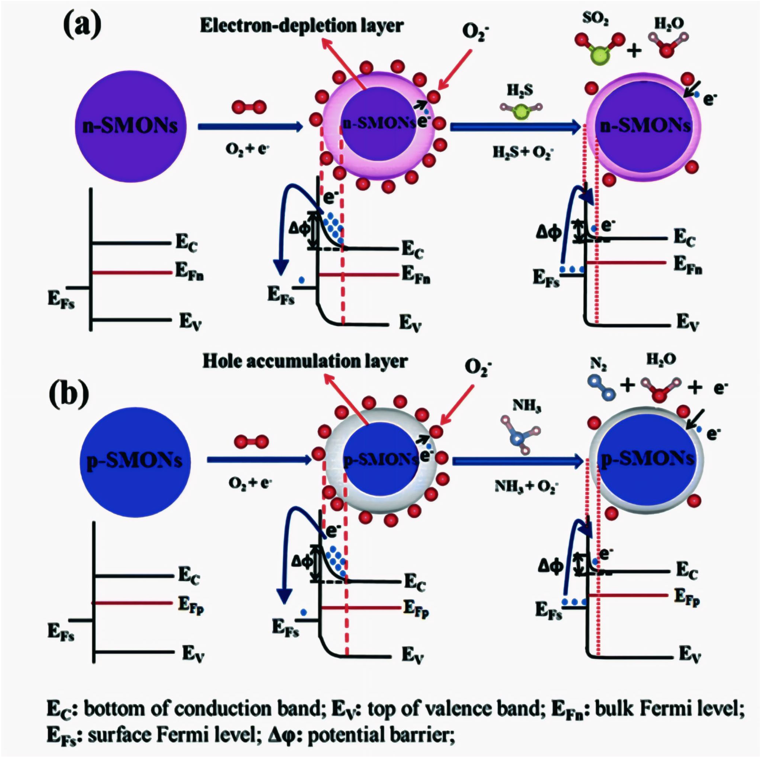
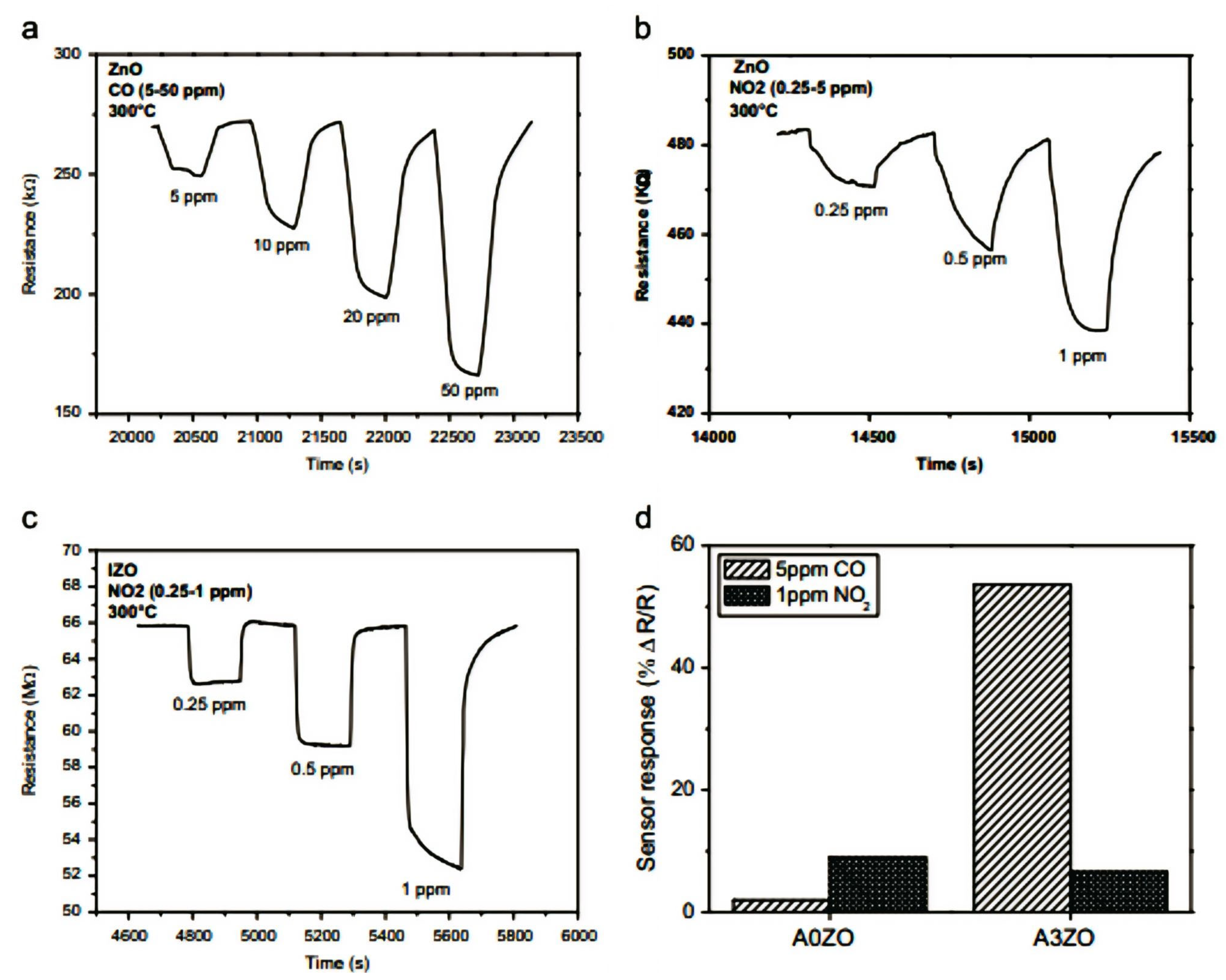
  • Rare-earth-doped ZnO sensor performance and gas selectivity:
Figure 10 presents the gas response of ZnO and Indium-doped ZnO (IZO) sensors at 300 °C, showing their effectiveness in detecting CO and NO2 gases. The performance comparison highlights the role of doping (In-doping in IZO) in enhancing the gas sensitivity and response time. ZnO sensors (Figure 10a,b) show a clear resistance change in response to varying CO and NO2 concentrations, demonstrating a high sensitivity and fast response times. IZO sensors (Figure 10c) exhibit an even stronger detection capability for NO2, suggesting an improved performance due to Indium doping. The sensor response comparison (Figure 10d) confirms the higher selectivity and efficiency of IZO sensors for CO detection. ZnO sensors are extensively used in environmental monitoring, industrial safety, and medical applications because of their high sensitivity and low-cost fabrication. One of the major applications is the monitoring of harmful gases (NO2, CO, CH4, and NH3) in cities, which is employed in fire protection systems and chemical process monitoring to identify dangerous gas leaks and is embedded in smart home devices and wearable health monitors for ongoing air quality monitoring. The ZnO is compared with SnO2 and WO3, which are also widely used in gas sensing applications, as mentioned in Table 7. The comparison of different rare-earth-doped ZnO, SnO2, and WO3 for gas sensor applications is mentioned in Table 8.
Chi-Jung Chang et al. examined a Ce-doped ZnO nanorod for low power consumption and low operating temperature portable NO2 gas sensor applications [98]. A study reported by Ahmad Umar et al. also supports the fact that Ce is a promising material to improve the performance of ZnO-based NO2 gas sensors. They have observed the best response for the 0.5% doped Ce nanostructure prepared by the hydrothermal method [99]. Gd-, Nd-, and Sm-doped ZnO thin films have been studied for room-temperature ammonia gas sensors. The result indicates that a fast response can be observed for 3% Nd doping with response–recovery times of 43 s and 12 s for 25 ppm of NH3 gas at room temperature [48]. Anita Hastir et al. studied Tb-, Dy-, and Er-doped ZnO prepared by the co-precipitation method for ethanol and acetone gas sensing applications. Doping in ZnO causes a high surface basicity, increased surface area, morphological changes, and oxygen vacancies, which enhance room-temperature sensing in doped ZnO [100]. Ce-, Eu-, and Er-doped ZnO nanowires synthesized by the solvothermal route have been reported by Sikai Zhao et al. for ethanol gas sensing. The best performance was observed for the 1% Ce-doped ZnO sample [101]. The Tb-, Er-, and Yb-doped ZnO prepared by the co-precipitation method have been explored for ammonia gas sensing applications. Among all prepared samples, the Tb-doped ZnO sample had the highest gas response value of 609% and a better response/recovery time of 7.64/4.87 s at ambient temperature for ammonia sensing [102].
Figure 10. ZnO-based gas sensor response at different concentrations of CO (a) and NO2 (b) (at 300 °C); IZO-based sensor response at different concentrations of NO2 at 300 °C (c), and comparison of sensor response based on AOZO and A3Z0 material for CO (d) and NO2 gas sensing (d) (reproduced with the permission of ref. [103], Elsevier, 2014).
Photonics 12 00454 g010
Table 7. Comparison of ZnO with other gas sensing materials.
PropertyZnO-Based Gas Sensors [104]SnO2-Based Gas Sensors [105,106]WO3-Based Gas Sensors [107]
Bandgap~3.37 eV~3.6 eV~2.6 eV
SensitivityHigh sensitivity to reducing gasesHigh sensitivity to reducing gasesHigh sensitivity to oxidizing gases
Response TimeFast response time due to high electron mobilityModerate response time, but fast in some formsSlower response due to lower electron mobility
SelectivityHigh selectivity with surface modification and dopingIt can be modified for selectivity, but generally less selectiveHigh selectivity for oxidizing gasses
FabricationEasy to fabricate, especially in nanostructured formsEasy to fabricate, commonly used in thin filmsRequires more advanced fabrication techniques for thin films
CostLow-cost, easily available materialsLow to moderate cost, widely used in commercial sensorsHigher cost, due to the more complex fabrication process
Environmental StabilityGood, with chemical stabilityGood, but may degrade under harsh conditionsGood stability, especially for high-temperature operations
Power consumptionLow power consumptionLow power consumptionModerate to high power consumption, depending on the configuration
Detection RangeCan detect a wide range of gasesPrimarily used for detecting reducing gasesPrimarily used for detecting oxidizing gases
Temperature sensitivityPerformance varies with temperature; typically requires heatingCan operate at high temperatures, often requires heatingCan operate at lower temperatures, but still requires heating
ApplicationsEnvironmental monitoring, industrial safety, healthcare, and smart homesEnvironmental monitoring, industrial safety, and automotive sensorsEnvironmental monitoring, automotive, and air quality monitoring
LimitationsPerformance affected by humidity, needs surface modification for selectivityLimited by surface sensitivity, may require complex circuitrySlower response, less suitable for real-time monitoring.
Table 8. Comparison of different rare-earth-doped ZnO, SnO2, and WO3 for gas sensing applications.
PropertyRare-Earth-Doped ZnO-Based Gas Sensor [108]Rare-Earth-Doped SnO2-Based Gas Sensor [109]Rare-Earth-Doped WO3-Based Gas Sensor [110]
Band gap~3.1–3.4~3.6~2.6–2.8
Key Target GasesNO2, H2, CO, and ethanolCO, CH4, H2SNH3, NO2, and acetone
Operating Temperature200–400 °C (lower with RE doping)150–350 °C (RE reduces optimal temp)250–450 °C (RE enhances low-temp response)
SensitivityHigh (e.g., ZnO:La for NO2 ~10 ppm detection)Very high (SnO2: Nd for H2 ~1 ppm)Moderate (WO3: Eu for NH3 ~5 ppm)
MechanismRE alters O2 adsorption and charge transfer (n-type)RE creates oxygen vacancies (n-type)RE promotes surface acidity (n/p-type)

3.6.5. ZnO-Based UV Radiation Detector

Rare-earth-doped Zinc Oxide (ZnO) is a developing material in the field of optoelectronics, especially in applications involving the re-emission of UV light. By the introduction of rare-earth elements, such as Europium (Eu), Terbium (Tb), or Dysprosium (Dy), into the ZnO host, the material can be endowed with improved luminescent behavior. The dopants enable ZnO to absorb ultraviolet (UV) radiation and re-emit it efficiently at visible wavelengths, which makes the material suitable for applications in light-emitting devices, phosphors, and sensors. The market potential of rare-earth-doped ZnO is high because of its prospects in numerous applications including UV sensors, solid-state lighting, and display technologies. The material’s capability to efficiently convert UV light into visible light provides opportunities in applications from health monitoring (detection of UV light) to energy-saving lighting solutions.
UV detectors work through the photoelectric effect, with the UV light driving electrons from the valence to the conduction band and thus creating electron–hole pairs responsible for a measurable current. A detector’s efficiency is how it can absorb the UV photons and transfer them to charge carriers. ZnO’s wide bandgap (~3.37 eV) is the reason why ZnO is an ideal material to absorb UV photons and thereby function very efficiently at detecting the wavelengths of UV-A, UV-B, and UV-C88. Upon the absorption of UV photons, ZnO can provide enough incoming energy to push electrons over the bandgap and generate a measurable charge flow. The excellent electron mobility of ZnO allows for a quick response, which is convenient for real-time UV sensing for environmental and security purposes. The high stability and the low cost of the fabrication of ZnO make it even more practical for use in wearable UV sensors, radiation monitor systems, and industrial safety tools.
The performance of ZnO-based UV detectors improves significantly when ZnO is engineered into nanostructures, such as nanowires, nanorods, and thin films. These structures enhance UV absorption and charge carrier separation through two mechanisms: increased surface area and a higher surface-to-volume ratio enables a more efficient UV absorption, improving sensitivity. Furthermore, nanostructured ZnO increases light–matter interactions, extending carrier lifetimes and boosting the detector efficiency [111]. In addition, doping adjustments enable ZnO UV detectors to adjust the spectral sensitivity and enhance the photo response. Experiments validate that ZnO retains its efficiency under varied environmental conditions and is thus a material of choice for biological and chemical UV sensing purposes, such as pathogen detection and air quality monitoring. Fabrication and Semiconductor Design:
The fabrication process uses diffusion techniques, selective layer deposition techniques, and radio frequency (RF) magnetron sputtering to enable the controlled growth of ZnO films. The n-type and p-type ZnO thin films are grown on a semi-insulating GaAs substrate as part of the semiconductor processing steps for ZnO-based UV detectors, as illustrated in Figure 11a. As seen in Figure 11b, the measurements setup includes a final semiconductor parameter analyzer that evaluates film properties by taking light absorption and charge transport measurements.
The comparison of the UV detection using ZnO, GaN, and SiC materials is presented in Table 9. ZnO competes with GaN and SiC as a material for UV detection, with distinct advantages in cost, fabrication, and performance. The comparison of rare-earth-doped ZnO, GaN, and SiC materials for UV light detection is presented in Table 10.
Table 9. Comparison of rare-earth-doped ZnO, GaN, and SiC for UV light detection.
PropertyZnO-Based [112]GaN-Based [113]SiC Based [114]
Bandgap~3.37 eV~3.4 eV~3.26 eV
UV Detection RangeUV-A, UV-B, and some UV-CPrimarily UV-C and UV-BUV-B and UV-C
Response TimeFast, high electron mobility for quick detectionVery fat response timeModerate response time
SensitivityHigh sensitivity, especially in UV-A and UV-B regionsVery high sensitivity, particularly in UV-CHigh sensitivity, especially in UV-C
CostLow costHigher costModerate cost
Fabrication EaseEasy to fabricateRequires advanced fabrication techniquesMore complex fabrication
Fabrication CostLow, cost-effective for mass productionExpensive due to manufacturing complexityModerate, more affordable than GaN but higher than ZnO
Table 10. Comparison of rare-earth-doped ZnO with GaN and SiC for UV light detection.
PropertyRare-Earth-Doped ZnO [115]Rare-Earth-Doped GaN [116]Rare-Earth-Doped SiC [117]
Band gap~3.1–3.4 (RE tunes responsivity in UV-A/B)~3.4 (direct; RE extends to UV-C)~3.2 (4H-SiC); RE enhances deep-UV response
Detection range (nm)300–400 nm (UV-A/B)200–365 nm (UV-B/C)200–400 nm (UV-C to A)
Response time~10–100 ms~1–50 ns~10–500 ns
The future potential of rare-earth-doped ZnO for UV detection is immense and promising. With continued progress in doping methods and material optimization, ZnO’s performance for highly selective and sensitive UV detection will improve further. As rare-earth doping continues to evolve, the material’s efficiency, emission wavelengths, and energy conversion characteristics will improve further, making it suitable for more accurate and reliable UV detection systems. The need for energy-efficient, high-performance materials for applications in fields like environmental monitoring, healthcare, and security will propel the broad use of ZnO-based sensors. Moreover, the scalability, simplicity of synthesis, and low cost of ZnO make it possible to be produced on a large scale for commercial use, ranging from portable UV detectors to integrated sensing devices in smart technology. In the future, rare-earth-doped ZnO will potentially become a foundation for next-generation optoelectronic devices, revolutionizing UV detection technologies and gaining new applications in areas like wearable sensors, aerospace, and industrial safety systems [118].
Rare earth-based ZnO UV detectors have been reported by some authors in the last few years. The incorporation of rare earth causes an increase in the defect concentration and oxygen vacancies. Such a change in the lattice supports the UV sensing mechanism and improves the performance of the device. In our previous work, we have reported on a doped ZnO thin film co-doped with Li for UV detector applications. The presence of Li helps to improve the performance without deformations in structure. The result indicates that the photocurrent value increases twice in Eu1%Li1%-doped ZnO thin films (6.75 μA) as compared to pure ZnO (3.14 μA) at a 4.0 V bias voltage under the UV irradiation of a 325 nm wavelength [119]. In another work we have explored a Dy-doped ZnO thin film prepared by spin coating with an improved sensitivity and detectivity for UV detector applications. The result suggests, under UV irradiation a 325 nm wavelength, the photocurrent value of the Dy-doped ZnO is 105.54 μA at 4.5 V, which is 31 times greater than that of the un-doped ZnO thin film (3.39 μA) [120].

3.6.6. ZnO-Based Temperature Sensor

The temperature sensor is an important device to reflect the safe operation of the cable. For power cables, a temperature variation of 1 °C can cause failure in cable operations. ZnO has been explored as a promising material. The metal oxides of Manganese, Nickel, and Cobalt have been explored for temperature sensing device fabrication. In the last few years, ZnO has emerged as a potential candidate for temperature sensing applications due to its ability to convert the temperature signal into an electrical signal. The electrical conductivity and resistivity of semiconductors (ZnO) vary with temperature, which makes it a preferable candidate for temperature sensing. ZnO has a negative temperature coefficient, i.e., its resistivity decreases with temperature. Fei Xue et al. have reported ZnO thin films deposited by the wet chemical deposition method as a potential candidate for temperature sensor applications. In addition, the study suggests that the piezotronics effect can be used for an improved temperature sensing of ZnO nanowires [121]. Sameer A Hasaan et al. reported a flexible and wearable temperature sensor based on a ZnO thin film fabricated by DC sputtering techniques. The flexible device fabricated by the authors has been studied in flat and curved conditions for temperature sensing [122]. The work on a ZnO nanowire deposited on a SiO2 substrate fabricated by the thermal chemical deposition method indicates a variation in the current for temperature sensing in the range from 90 to 380 K [123]. It has been observed that a ZnO composite graphene can be used for optical fiber temperature sensors. The ZnO graphene composite prepared by the hydrothermal method plays a crucial role in improving the performance of temperature sensors [124]. Xinqin Liao et al. reported a stretchable ZnO fiber temperature sensor with a sensitivity of 39.3% °C−1 [125]. The defect concentration in ZnO also affects the temperature sensing efficiency. Junal Jia et al. reported a ZnO thin film for low temperature sensors. The prepared thin film was treated with oxygen plasma to control the defects [125].

3.6.7. ZnO Mechano-Luminescence

Mechano-luminescence (ML) shows the emission of light by applying mechanical grinding, crushing, or rubbing to materials. Luminescence produced by mechanical methods in materials have been considered as an alternative for the upcoming energy crisis. The conversion of stress into light is a promising feature of materials that can be improved to achieve desired applications. ZnO has been reported as a candidate for mechano-luminescence properties. ZnO-based ML may have potential applications in flexible and stretchable optoelectronics devices, next-generation self-powered displays devices, skin electronic devices, and anti-counterfeiting devices. These applications do not require any external light/electric-incentive sources, if we utilize the ML feature of ZnO. The literature supports that the incorporation of other compositions can improve the output of ZnO. Leipeng Li et al. reported a ZnF2:Mn2+-embedded ZnO shows a reddish-yellow ML with the application of stress [126]. Pyramids like ZnO synthesized by the hydrothermal method have been reported by Ya-Chuan Liang et al. for the highly sensitive, wireless detection of mechanical stimuli. The study suggests that the high sensitivity achieved by the electron ejection process in crystal boundaries can be used for hearing impaired devices [40]. The study suggests that the ML in ZnO is controlled by three mechanisms, namely impact-induced, friction-induced, and pressure-induced ML. The first one is impacting-induced ML, which is generated due to sudden stress. Sudden stress like, dropping and hitting, can cause the generation of piezoelectric fields to induce light flashes. ML in most sensing applications in generated by sliding or rubbing, which is known as friction-induced ML. The application of pressure or stretching on ZnO causes gradual deformation, with preprocessed or modulated light. It has been observed that the output of ML in ZnO can be enhanced by variations in the crystalline structure, morphology, doping, defect concentration, and hybrid structure. Highly a sensitive visible emission has potential applications in smart sensing systems, damage detection, and energy harvesting mediated by piezo-photonic mechanisms and flexible electronics.

4. Conclusions

Rare-earth doping has emerged as a potential method to improve the optoelectronic characteristics of ZnO to make it universally applicable in UV photodetectors, LEDs, gas sensors, and TCOs. The rare-earth-element doping into the ZnO lattice profoundly alters its structural, optical, and electronic characteristics, resulting in an enhanced crystallinity, diminished lattice strain, and increased photoluminescence. Furthermore, rare-earth doping efficiently modulates the bandgap and charge carrier behavior, enhancing device performances in future optoelectronic devices. Despite these developments, issues like solubility constraints, structural distortions at high doping concentrations, and fabrication complexities must be explored further. Future work should emphasize doping concentration optimization, co-doping approaches, and new synthesis methods to enhance the rare-earth integration into ZnO matrices. By overcoming such challenges, rare-earth-doped ZnO may realize its true potential as an advanced electronic and photonic high-performance material.

Author Contributions

Conceptualization S.S. and J.G.; methodology, S.S.; formal analysis, S.K. (Sanjeev Kumar) and S.K. (Sandeep Kaushal); investigation, writing—original draft preparation P.K. and M.M.; writing—review and editing, P.K. and S.S.; visualization, G.S. and I.R., supervision, P.K. All authors have read and agreed to the published version of the manuscript.

Funding

The authors declare no external funding and support.

Conflicts of Interest

The authors declare no conflicts of interest.

References

  1. Chandekar, K.V.; Shkir, M.; Khan, A.; Al-Shehri, B.M.; Hamdy, M.S.; AlFaify, S.; El-Toni, M.A.; Aldalbahi, A.; Ansari, A.A.; Ghaithan, H. A Facile One-Pot Flash Combustion Synthesis of La@ZnO Nanoparticles and Their Characterizations for Optoelectronic and Photocatalysis Applications. J. Photochem. Photobiol. A Chem. 2020, 395, 112465. [Google Scholar] [CrossRef]
  2. Raha, S.; Ahmaruzzaman, M. ZnO Nanostructured Materials and Their Potential Applications: Progress, Challenges and Perspectives. Nanoscale Adv. 2022, 4, 1868–1925. [Google Scholar] [CrossRef] [PubMed]
  3. Ong, C.B.; Ng, L.Y.; Mohammad, A.W. A Review of ZnO Nanoparticles as Solar Photocatalysts: Synthesis, Mechanisms and Applications. Renew. Sustain. Energy Rev. 2018, 81, 536–551. [Google Scholar] [CrossRef]
  4. Sahu, S.; Bhattacharjee, M. Nanostructured ZnO Thin Film-Based Flexible Printed Sensor for High-Performance UV Detection. Sens. Actuators A Phys. 2025, 383, 116196. [Google Scholar] [CrossRef]
  5. Huong, T.T.T.; Sa, N.T.; Thuy, N.T.M.; Hao, P.V.; Thao, N.H.; Hien, N.T.; Ca, N.X. Eu3+-Doped ZnO Quantum Dots: Structure, Vibration Characteristics, Optical Properties, and Energy Transfer Process. Nanoscale Adv. 2024, 7, 909–921. [Google Scholar] [CrossRef]
  6. Girish Kumar, S.; Kavitha, R. Lanthanide Ions Doped ZnO Based Photocatalysts. Sep. Purif. Technol. 2021, 274, 118853. [Google Scholar] [CrossRef]
  7. Sanakousar, F.M.; Vidyasagar, C.; Jiménez-Pérez, V.M.; Prakash, K. Recent Progress on Visible-Light-Driven Metal and Non-Metal Doped ZnO Nanostructures for Photocatalytic Degradation of Organic Pollutants. Mater. Sci. Semicond. Process 2022, 140, 106390. [Google Scholar] [CrossRef]
  8. Ren, J.; Wu, J.X.; Liu, P.P. Controlling the Electronic and Magnetic Properties of ZnO Monolayer by Rare-Earth Atoms Substitutional Doping. Phys. B Condens. Matter 2023, 652, 414661. [Google Scholar] [CrossRef]
  9. Silva, W.F.; Silva, A.C.A.; Jacinto, C. Applications of Luminescence in Quantum-Dot- and Rare-Earth-Doped Semiconductor Nanostructures. Mod. Lumin. Fundam. Concepts Mater. Appl. 2025, 2, 31–67. [Google Scholar] [CrossRef]
  10. Khuili, M.; Fazouan, N.; Abou El Makarim, H.; Atmani, E.H.; Rai, D.P.; Houmad, M. First-Principles Calculations of Rare Earth (RE=Tm, Yb, Ce) Doped ZnO: Structural, Optoelectronic, Magnetic, and Electrical Properties. Vacuum 2020, 181, 109603. [Google Scholar] [CrossRef]
  11. Achehboune, M.; Khenfouch, M.; Boukhoubza, I.; Leontie, L.; Doroftei, C.; Carlescu, A.; Bulai, G.; Mothudi, B.; Zorkani, I.; Jorio, A. Microstructural, FTIR and Raman Spectroscopic Study of Rare Earth Doped ZnO Nanostructures. Mater. Today Proc. 2022, 53, 319–323. [Google Scholar] [CrossRef]
  12. Thangeeswari, T.; Parthipan, G.; Shanmugan, S. Raju Synthesize of Gadolinium-Doped ZnO Nano Particles for Energy Applications by Enhance Its Optoelectronic Properties. Mater. Today Proc. 2021, 34, 448–452. [Google Scholar] [CrossRef]
  13. Ben Haj Othmen, W.; Ben Ali, M.; Bouslama, W.; Elhouichet, H. Solar Driven Photocatalytic Properties of Sm3+ Doped ZnO Nanocrystals. Ceram. Int. 2020, 46, 18878–18887. [Google Scholar] [CrossRef]
  14. Zamiri, R.; Lemos, A.F.; Reblo, A.; Ahangar, H.A.; Ferreira, J.M.F. Effects of Rare-Earth (Er, La and Yb) Doping on Morphology and Structure Properties of ZnO Nanostructures Prepared by Wet Chemical Method. Ceram. Int. 2014, 40, 523–529. [Google Scholar] [CrossRef]
  15. Ranjith Kumar, D.; Ranjith, K.S.; Rajendra Kumar, R.T. Structural, Optical, Photocurrent and Solar Driven Photocatalytic Properties of Vertically Aligned Samarium Doped ZnO Nanorod Arrays. Optik 2018, 154, 115–125. [Google Scholar] [CrossRef]
  16. Amira, G.; Chaker, B.; Habib, E. Spectroscopic Properties of Dy3+ Doped ZnO for White Luminescence Applications. Spectrochim. Acta A Mol. Biomol. Spectrosc. 2017, 177, 164–169. [Google Scholar] [CrossRef]
  17. Selvaraj, S.; Vangari, G.A.; Mohan, M.K.; Ponnusamy, S.; Muthamizchelvan, C. Facile Synthesis of Sm Doped ZnO Nanoflowers by Co-Precipitation Method for Enhanced Photocatalytic Degradation of MB Dye under Sunlight Irradiation. Ceram. Int. 2022, 48, 29049–29058. [Google Scholar] [CrossRef]
  18. López-Mena, E.R.; Jiménez-Sandoval, S.J.; Jiménez-Sandoval, O. Samarium-Doped ZnO Thin Films Synthesized by Sol-Gel: Structural, Optical and Electrical Properties. Mater. Sci. Semicond. Process 2021, 126, 105648. [Google Scholar] [CrossRef]
  19. Manikandan, A.; Manikandan, E.; Meenatchi, B.; Vadivel, S.; Jaganathan, S.K.; Ladchumananandasivam, R.; Henini, M.; Maaza, M.; Aanand, J.S. Rare Earth Element (REE) Lanthanum Doped Zinc Oxide (La: ZnO) Nanomaterials: Synthesis Structural Optical and Antibacterial Studies. J. Alloys Compd. 2017, 723, 1155–1161. [Google Scholar] [CrossRef]
  20. Sikdar, M.K.; Ghorai, G.; Senapati, T.R.; Sahoo, P.K. Modulation of Bandgap and Electrical Conductivity in Europium Doped Single ZnO Nanorod Device. J. Alloys Compd. 2022, 913, 165179. [Google Scholar] [CrossRef]
  21. Korsunska, N.; Borkovska, L.; Polischuk, Y.; Kolomys, O.; Lytvyn, P.; Markevich, I.; Strelchuk, V.; Kladko, V.; Melnichuk, O.; Melnichuk, L.; et al. Photoluminescence, Conductivity and Structural Study of Terbium Doped ZnO Films Grown on Different Substrates. Mater. Sci. Semicond. Process 2019, 94, 51–56. [Google Scholar] [CrossRef]
  22. Karakaya, S.; Kaba, L. Photocatalytic Activity of Rare Earth Elements (Gd and Ce) Co-Doped ZnO Nanostructured Films. Ceram. Int. 2024, 50, 30743–30753. [Google Scholar] [CrossRef]
  23. Thobega, M.; Maabong-Tau, K.; Lefatshe, K.; Muiva, C. Study of Structural, Optical and Electrical Properties of Nickel Doped ZnO (Ni–ZnO) Nanorods Grown by Chemical Bath Deposition. Phys. B Condens. Matter 2024, 673, 415500. [Google Scholar] [CrossRef]
  24. Dole, B.N.; Mote, V.D.; Huse, V.R.; Purushotham, Y.; Lande, M.K.; Jadhav, K.M.; Shah, S.S. Structural Studies of Mn Doped ZnO Nanoparticles. Curr. Appl. Phys. 2011, 11, 762–766. [Google Scholar] [CrossRef]
  25. Nair, M.G.; Nirmala, M.; Rekha, K.; Anukaliani, A. Structural, Optical, Photo Catalytic and Antibacterial Activity of ZnO and Co Doped ZnO Nanoparticles. Mater. Lett. 2011, 65, 1797–1800. [Google Scholar] [CrossRef]
  26. Alev, O.; Ergün, İ.; Özdemir, O.; Arslan, L.Ç.; Büyükköse, S.; Öztürk, Z.Z. Enhanced Ethanol Sensing Performance of Cu-Doped ZnO Nanorods. Mater. Sci. Semicond. Process 2021, 136, 106149. [Google Scholar] [CrossRef]
  27. Srivastava, A.K.; Deepa, M.; Bahadur, N.; Goyat, M.S. Influence of Fe Doping on Nanostructures and Photoluminescence of Sol–Gel Derived ZnO. Mater. Chem. Phys. 2009, 114, 194–198. [Google Scholar] [CrossRef]
  28. Khan, I.; Khan, S.; Nongjai, R.; Ahmed, H.; Khan, W. Structural and Optical Properties of Gel-Combustion Synthesized Zr Doped ZnO Nanoparticles. Opt. Mater. 2013, 35, 1189–1193. [Google Scholar] [CrossRef]
  29. Lupan, O.; Pauporté, T.; Viana, B.; Aschehoug, P.; Ahmadi, M.; Cuenya, B.R.; Rudzevich, Y.; Lin, Y.; Chow, L. Eu-Doped ZnO Nanowire Arrays Grown by Electrodeposition. Appl. Surf. Sci. 2013, 282, 782–788. [Google Scholar] [CrossRef]
  30. Bhatia, S.; Verma, N.; Kumar, R. Morphologically-Dependent Photocatalytic and Gas Sensing Application of Dy-Doped ZnO Nanoparticles. J. Alloys Compd. 2017, 726, 1274–1285. [Google Scholar] [CrossRef]
  31. Malyutina-Bronskaya, V.; Zalesski, V.; Zhyhulin, D.; Mudryi, A. Structural, Optical and Photoelectric Properties of Tb Doped ZnO Thin Films for Device Applications. Opt. Mater. 2022, 127, 112305. [Google Scholar] [CrossRef]
  32. Phuruangrat, A.; Yayapao, O.; Thongtem, T.; Thongtem, S. Preparation, Characterization and Photocatalytic Properties of Ho Doped ZnO Nanostructures Synthesized by Sonochemical Method. Superlattices Microstruct. 2014, 67, 118–126. [Google Scholar] [CrossRef]
  33. Fabbiyola, S.; Sailaja, V.; Kennedy, L.J.; Bououdina, M.; Judith Vijaya, J. Optical and Magnetic Properties of Ni-Doped ZnO Nanoparticles. J. Alloys Compd. 2017, 694, 522–531. [Google Scholar] [CrossRef]
  34. Wu, C.; Shen, L.; Zhang, Y.C.; Huang, Q. Solvothermal Synthesis of Cr-Doped ZnO Nanowires with Visible Light-Driven Photocatalytic Activity. Mater. Lett. 2011, 65, 1794–1796. [Google Scholar] [CrossRef]
  35. Kumar, S.; Kaur, P.; Chen, C.L.; Thangavel, R.; Dong, C.L.; Ho, Y.K.; Lee, J.F.; Chan, T.S.; Chen, T.K.; Mok, B.H.; et al. Structural, Optical and Magnetic Characterization of Ru Doped ZnO Nanorods. J. Alloys Compd. 2014, 588, 705–709. [Google Scholar] [CrossRef]
  36. Çolak, H.; Karaköse, E.; Sungür, Ç. Niobium Doping Effect on Electrical and Optical Properties of ZnO Nanorods Produced by Ultrasonic Spray Pyrolysis. Phys. B Condens. Matter 2023, 671, 415455. [Google Scholar] [CrossRef]
  37. Naeem, H.M.; Ijaz, S.; Abbas, M.H.; Ahmed, Y.; Rehman, N.; Park, T.J.; Basit, M.A. HF-Based Surface Modification for Enhanced Photobiological and Photochemical Performance of ZnO and ZnO/CdS Hierarchical Structures. Mater. Chem. Phys. 2020, 252, 123190. [Google Scholar] [CrossRef]
  38. Saravanan, R.; Gupta, V.K.; Prakash, T.; Narayanan, V.; Stephen, A. Synthesis, Characterization and Photocatalytic Activity of Novel Hg Doped ZnO Nanorods Prepared by Thermal Decomposition Method. J. Mol. Liq. 2013, 178, 88–93. [Google Scholar] [CrossRef]
  39. Kotresh, M.G.; Patil, M.K.; Inamdar, S.R. Reaction Temperature Based Synthesis of ZnO Nanoparticles Using Co-Precipitation Method: Detailed Structural and Optical Characterization. Optik 2021, 243, 167506. [Google Scholar] [CrossRef]
  40. Liang, Q.; Qiao, F.; Cui, X.; Hou, X. Controlling the Morphology of ZnO Structures via Low Temperature Hydrothermal Method and Their Optoelectronic Application. Mater. Sci. Semicond. Process 2019, 89, 154–160. [Google Scholar] [CrossRef]
  41. Seleš, P.; Vengust, D.; Radošević, T.; Kocijan, M.; Einfalt, L.; Kurtjak, M.; Shvalya, V.; Knaflič, T.; Bernik, S.; Omerzu, A.; et al. Altering Defect Population during the Solvothermal Growth of ZnO Nanorods for Photocatalytic Applications. Ceram. Int. 2024, 50, 26819–26828. [Google Scholar] [CrossRef]
  42. Ul Haq, B.; Ahmed, R.; Shaari, A.; Ali, N.; Al-Douri, Y.; Reshak, A.H. Comparative Study of Fe Doped ZnO Based Diluted and Condensed Magnetic Semiconductors in Wurtzite and Zinc-Blende Structures by First-Principles Calculations. Mater. Sci. Semicond. Process 2016, 43, 123–128. [Google Scholar] [CrossRef]
  43. Xiao, Y.; Ge, S.; Xi, L.; Zuo, Y.; Zhou, X.; Zhang, B.; Zhang, L.; Li, C.; Han, X.; Wen, Z. Room Temperature Ferromagnetism of Mn-Doped SnO2 Thin Films Fabricated by Sol–Gel Method. Appl. Surf. Sci. 2008, 254, 7459–7463. [Google Scholar] [CrossRef]
  44. Krishna, M.S.; Singh, S.; Batool, M.; Fahmy, H.M.; Seku, K.; Shalan, A.E.; Lanceros-Mendez, S.; Zafar, M.N. A Review on 2D-ZnO Nanostructure Based Biosensors: From Materials to Devices. Mater. Adv. 2023, 4, 320–354. [Google Scholar] [CrossRef]
  45. Comini, E.; Baratto, C.; Faglia, G.; Ferroni, M.; Vomiero, A.; Sberveglieri, G. Quasi-One Dimensional Metal Oxide Semiconductors: Preparation, Characterization and Application as Chemical Sensors. Prog. Mater. Sci. 2009, 54, 1–67. [Google Scholar] [CrossRef]
  46. Nguyen, D.T.C.; Nguyen, N.T.T.; Nguyen, T.T.T.; Tran, T. Van Recent Advances in the Biosynthesis of ZnO Nanoparticles Using Floral Waste Extract for Water Treatment, Agriculture and Biomedical Engineering. Nanoscale Adv. 2024, 6, 4047–4061. [Google Scholar] [CrossRef]
  47. Shivaraj, B.; Hareeshanaik, S.; Vishnu, G.; Prabhakara, M.C.; BhojyaNaik, H.S. Fabrication of Ce-Doped ZnO Nanorods as Efficient Materials for Photocatalytic, Bio-Sensing and Antibacterial Applications. Mater. Sci. Eng. B 2025, 314, 118029. [Google Scholar] [CrossRef]
  48. Kasirajan, K.; Bruno Chandrasekar, L.; Maheswari, S.; Karunakaran, M.; Shunmuga Sundaram, P. A Comparative Study of Different Rare-Earth (Gd, Nd, and Sm) Metals Doped ZnO Thin Films and Its Room Temperature Ammonia Gas Sensor Activity: Synthesis, Characterization, and Investigation on the Impact of Dopant. Opt. Mater. 2021, 121, 111554. [Google Scholar] [CrossRef]
  49. Pratomo, U.; Fransisca, N.; Adzani, M.D.; Irkham, I.; Sulaeman, A.P.; Eddy, D.R.; Mulyana, J.Y.; Primadona, I. Doping of Rare Earth Element: The Effects in Elevated Physical and Optical Properties of ZnO. Talanta Open 2025, 11, 100411. [Google Scholar] [CrossRef]
  50. Petersen, J.; Brimont, C.; Gallart, M.; Schmerber, G.; Gilliot, P.; Ulhaq-Bouillet, C.; Rehspringer, J.L.; Colis, S.; Becker, C.; Slaoui, A.; et al. Correlation of Structural Properties with Energy Transfer of Eu-Doped ZnO Thin Films Prepared by Sol-Gel Process and Magnetron Reactive Sputtering. J. Appl. Phys. 2010, 107, 123522. [Google Scholar] [CrossRef]
  51. Sharma, R.; Sehrawat, K.; Mehra, R.M. Epitaxial Growth of Highly Transparent and Conducting Sc-Doped ZnO Films on c-Plane Sapphire by Sol–Gel Process without Buffer. Curr. Appl. Phys. 2010, 10, 164–170. [Google Scholar] [CrossRef]
  52. Krishnaswamy, S.; Yashpal; Panigrahi, P.; Panigrahi, A.; Nagarajan, G.S. Investigation of the Optical Properties of Dy Doped ZnO/PVA Thin Film: White Light Emission for LED Application. Results Opt. 2025, 18, 100786. [Google Scholar] [CrossRef]
  53. Jayachandraiah, C.; Siva Kumar, K.; Krishnaiah, G.; Madhusudhana Rao, N. Influence of Dy Dopant on Structural and Photoluminescence of Dy-Doped ZnO Nanoparticles. J. Alloys Compd. 2015, 623, 248–254. [Google Scholar] [CrossRef]
  54. El Fidha, G.; Bitri, N.; Chaabouni, F.; Acosta, S.; Güell, F.; Bittencourt, C.; Casanova-Chafer, J.; Llobet, E. Physical and Photocatalytic Properties of Sprayed Dy Doped ZnO Thin Films under Sunlight Irradiation for Degrading Methylene Blue. RSC Adv. 2021, 11, 24917–24925. [Google Scholar] [CrossRef]
  55. Alasmari, A.; Awad, A.A.; Aboud, A.A. Investigating the Influence of Yttrium Doping on Physical Properties of ZnO Thin Films Deposited via Spray Pyrolysis. Opt. Mater. 2024, 148, 114899. [Google Scholar] [CrossRef]
  56. Sinha, N.; Ray, G.; Bhandari, S.; Godara, S.; Kumar, B. Synthesis and Enhanced Properties of Cerium Doped ZnO Nanorods. Ceram. Int. 2014, 40, 12337–12342. [Google Scholar] [CrossRef]
  57. Jia, T.; Wang, W.; Long, F.; Fu, Z.; Wang, H.; Zhang, Q. Synthesis, Characterization and Luminescence Properties of Y-Doped and Tb-Doped ZnO Nanocrystals. Mater. Sci. Eng. B 2009, 162, 179–184. [Google Scholar] [CrossRef]
  58. Singh, J.; Singh, G.P.; Kumar, S.; Jain, R.K.; Gasso, S.; Singh, B.; Singh, K.J.; Singh, A.; Singh, R.C. Probing Structural, Optical and Magnetic Properties of Sm-Doped ZnO Nanomaterials via Experimental and DFT Approach: Enhanced Photocatalytic Degradation and Antibacterial Performance. Colloids Surf. A Physicochem. Eng. Asp. 2023, 668, 131470. [Google Scholar] [CrossRef]
  59. Kumar, S.; Sahare, P.D. Nd-Doped ZnO as a Multifunctional Nanomaterial. J. Rare Earths 2012, 30, 761–768. [Google Scholar] [CrossRef]
  60. Wang, C.; Ma, S.; Sun, A.; Qin, R.; Yang, F.; Li, X.; Li, F.; Yang, X. Characterization of Electrospun Pr-Doped ZnO Nanostructure for Acetic Acid Sensor. Sens. Actuators B Chem. 2014, 193, 326–333. [Google Scholar] [CrossRef]
  61. Çolak, H.; Karaköse, E. Synthesis and Structural, Electrical, Optical Properties of Lu3+-Doped ZnO Nanorods. Mater. Sci. Semicond. Process 2019, 101, 230–237. [Google Scholar] [CrossRef]
  62. Khan, M.; Ali, R.; Nowsherwan, G.A.; Anwar, N.; Ahmed, M.; Ali, Q.; Ahmed, M.; Naseem, S.; Lee, S.-L.; Choi, J.R. Gd-Doped ZnO Nanoparticles: Structural, Morphological, and Optoelectronic Enhancements. Ceram. Int. 2025, 51, 14417–14429. [Google Scholar] [CrossRef]
  63. Çolak, H.; Karaköse, E. Tm-Doped ZnO Nanorods as a TCO for PV Applications. J. Rare Earths 2018, 36, 1067–1073. [Google Scholar] [CrossRef]
  64. Navarro-López, D.E.; Garcia-Varela, R.; Ceballos-Sanchez, O.; Sanchez-Martinez, A.; Sanchez-Ante, G.; Corona-Romero, K.; Buentello-Montoya, D.A.; Elías-Zuñiga, A.; López-Mena, E.R. Effective Antimicrobial Activity of ZnO and Yb-Doped ZnO Nanoparticles against Staphylococcus aureus and Escherichia coli. Mater. Sci. Eng. C 2021, 123, 112004. [Google Scholar] [CrossRef]
  65. Radić, N.; Stojadinović, S.; Ilić, M.; Kasalica, K.; Tsanev, A. Eu-Doped ZnO Coatings Prepared by Spray Pyrolysis for Photocatalytic Applications. Inorg. Chem. Commun. 2024, 167, 112822. [Google Scholar] [CrossRef]
  66. Mohamed, M.; Al–Naim, A.F.; Almohammedi, A.; Sedky, A. Comparative Investigation of Dielectric, Magnetic, and Adsorption Aspects of ZnO Nanoparticles Doped by Er or Nd. Results Phys. 2025, 69, 108113. [Google Scholar] [CrossRef]
  67. Anwar, M.; Kayani, Z.N.; Hassan, A.; Zeeshan, T.; Riaz, S.; Naseem, S. Enhancement in Photocatalytic Activity and Biological Properties of Sm Doped ZnO Nanostructures by the Increase in Sm Contents. Inorg. Chem. Commun. 2023, 158, 111431. [Google Scholar] [CrossRef]
  68. Phuruangrat, A.; Thamsukho, S.; Thongtem, T.; Thongtem, S. Combustion Synthesis and Analysis of Visible-Light-Driven Ho-Doped ZnO Photocatalytic Nanoparticles. Desalination Water Treat. 2022, 273, 212–220. [Google Scholar] [CrossRef]
  69. Luo, J.; Wang, Y.; Zhang, Q. Progress in Perovskite Solar Cells Based on ZnO Nanostructures. Sol. Energy 2018, 163, 289–306. [Google Scholar] [CrossRef]
  70. Zafar, M.; Kim, B.S.; Kim, D.H. Improvement in Performance of Inverted Organic Solar Cell by Rare Earth Element Lanthanum Doped ZnO Electron Buffer Layer. Mater. Chem. Phys. 2020, 240, 122076. [Google Scholar] [CrossRef]
  71. Oku, T.; Kakuta, N.; Kobayashi, K.; Suzuki, A.; Kikuchi, K. Fabrication and Characterization of TiO2-Based Dye-Sensitized Solar Cells. Prog. Nat. Sci. Mater. Int. 2011, 21, 122–126. [Google Scholar] [CrossRef]
  72. Mufti, N.; Amrillah, T.; Taufiq, A.; Sunaryono; Aripriharta; Diantoro, M.; Zulhadjri; Nur, H. Review of CIGS-Based Solar Cells Manufacturing by Structural Engineering. Sol. Energy 2020, 207, 1146–1157. [Google Scholar] [CrossRef]
  73. Simran; Kumar, P.; Tamanna; Kumar, S.; Kaur, H.; Kumar, A.; Kumar, A. Optimizing Photocatalysis: Tuning Europium Concentration in Zinc Oxide Nanoparticles for Superior Performance. Phys. B Condens. Matter 2025, 697, 416699. [Google Scholar] [CrossRef]
  74. Abdel-Latif, M.K.; Mobarak, M.; Revaprasadu, N.; Ashraf, A.H.; Othman, W.; Khalefa, M.M.; Aboud, A.A.; Ismail, M. Effect of Doping on the Structural, Optical and Electrical Properties of La-Doped ZnO Thin Films. J. Mater. Sci. Mater. Electron. 2023, 34, 254. [Google Scholar] [CrossRef]
  75. Faisal, M.; Ismail, A.A.; Ibrahim, A.A.; Bouzid, H.; Al-Sayari, S.A. Highly Efficient Photocatalyst Based on Ce Doped ZnO Nanorods: Controllable Synthesis and Enhanced Photocatalytic Activity. Chem. Eng. J. 2013, 229, 225–233. [Google Scholar] [CrossRef]
  76. D’Souza, L.P.; Shwetharani, R.; Amoli, V.; Fernando, C.A.N.; Sinha, A.K.; Balakrishna, R.G. Photoexcitation of Neodymium Doped TiO2 for Improved Performance in Dye-Sensitized Solar Cells. Mater. Des. 2016, 104, 346–354. [Google Scholar] [CrossRef]
  77. Barba-Nieto, I.; Caudillo-Flores, U.; Fernández-García, M.; Kubacka, A. Sunlight-Operated TiO2-Based Photocatalysts. Molecules 2020, 25, 4008. [Google Scholar] [CrossRef]
  78. Jayachithra, J.V.; Elampari, K.; Meena, M. Enhancing CIGS Solar Cell Performance with Erbium-Doped TiO2 Nanomaterial: Simulation Study. Artic. Indian J. Sci. Technol. 2023, 16, 3453. [Google Scholar] [CrossRef]
  79. Xiong, Z. Enhancing CIGS Solar Cell Performance by Down Conversion; The Chinese University of Hong Kong: Hong Kong, China, 2019. [Google Scholar]
  80. Kumar, V.; Ntwaeaborwa, O.M.; Soga, T.; Dutta, V.; Swart, H.C. Rare Earth Doped Zinc Oxide Nanophosphor Powder: A Future Material for Solid State Lighting and Solar Cells. ACS Photonics 2017, 4, 2613–2637. [Google Scholar] [CrossRef]
  81. Pandey, P.; Kurchania, R.; Haque, F.Z. Rare Earth Ion (La, Ce, and Eu) Doped ZnO Nanoparticles Synthesized via Sol-Gel Method: Application in Dye Sensitized Solar Cells. Opt. Spectrosc. 2015, 119, 666–671. [Google Scholar] [CrossRef]
  82. Mokgolo, P.J.; Gumede, T.P.; Ocaya, R.O.; Malevu, T.D. Enhancing Perovskite Solar Cells with Rare-Earth Metal Doped Zinc Oxide: A Review of Electron Mobility, Stability, and Photocarrier Recombination. Int. J. Energy Res. 2025, 2025, 4240199. [Google Scholar] [CrossRef]
  83. Sehgal, P.; Narula, A.K. Improved Optical, Electrochemical and Photovoltaic Properties of Dye-Sensitized Solar Cell Composed of Rare Earth-Doped Zinc Oxide. J. Mater. Sci. Mater. Electron. 2021, 32, 16612–16622. [Google Scholar] [CrossRef]
  84. Pearton, S.J.; Ren, F. Advances in ZnO-Based Materials for Light Emitting Diodes. Curr. Opin. Chem. Eng. 2014, 3, 51–55. [Google Scholar] [CrossRef]
  85. Mo, X.; Fang, G.; Long, H.; Li, S.; Huang, H.; Wang, H.; Liu, Y.; Meng, X.; Zhang, Y.; Pan, C. Near-Ultraviolet Light-Emitting Diodes Realized from n-ZnO Nanorod/p-GaN Direct-Bonding Heterostructures. J. Lumin. 2013, 137, 116–120. [Google Scholar] [CrossRef]
  86. Lu, Z.; Zhang, K.; Zhuang, J.; Lin, J.; Lu, Z.; Jiang, Z.; Lu, Y.; Chen, Z.; Guo, W. Recent Progress of InGaN-Based Red Light Emitting Diodes. Micro Nanostruct. 2023, 183, 207669. [Google Scholar] [CrossRef]
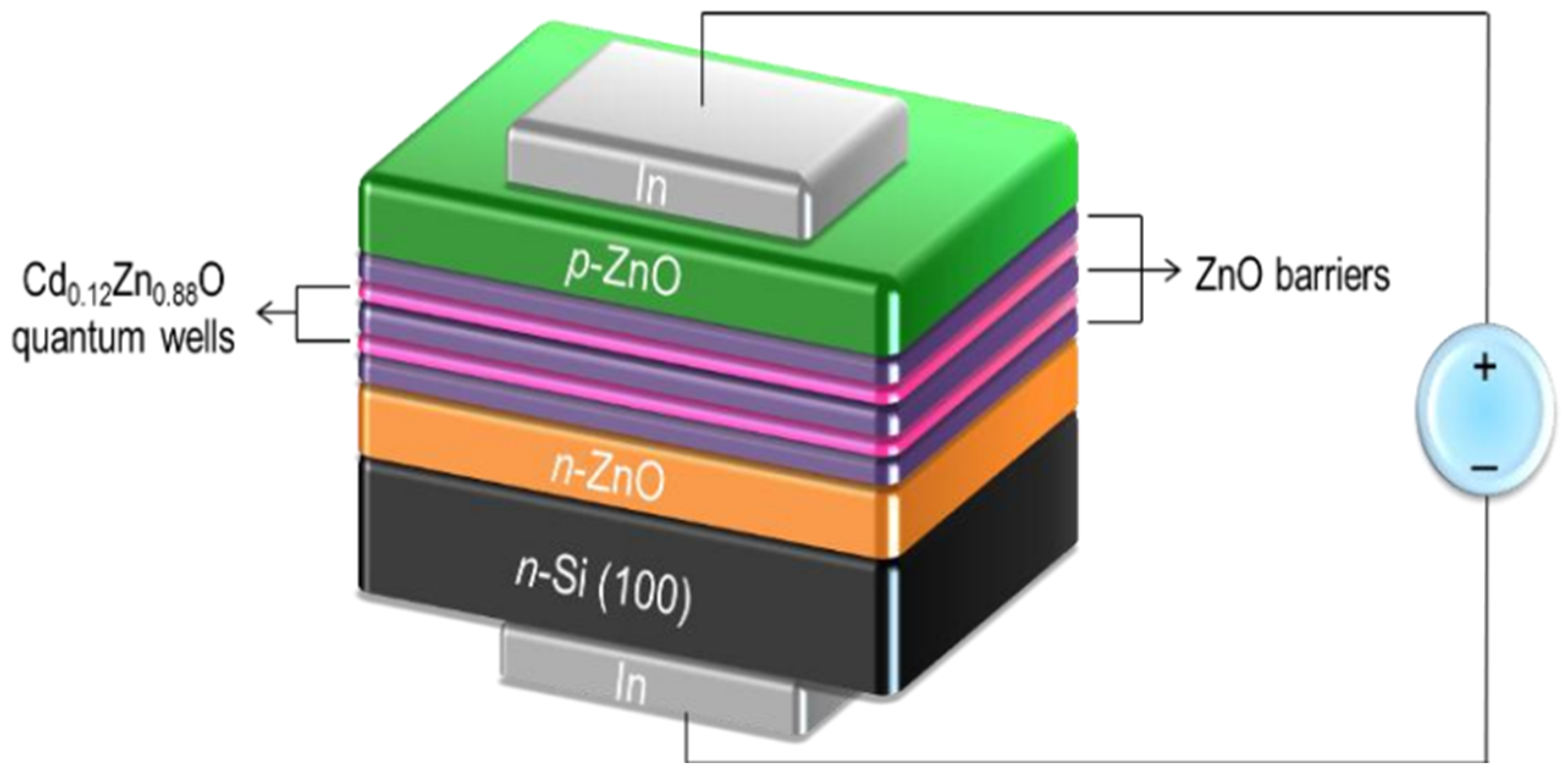
  87. Awasthi, V.; Pandey, S.K.; Verma, S.; Mukherjee, S. Room Temperature Blue LED Based on P-ZnO/(CdZnO/ZnO) MQWs/ n-ZnO. J. Lumin. 2016, 180, 204–208. [Google Scholar] [CrossRef]
  88. Edmond, J.; Abare, A.; Bergman, M.; Bharathan, J.; Bunker, K.L.; Emerson, D.; Haberern, K.; Ibbetson, J.; Leung, M.; Russel, P.; et al. High Efficiency GaN-Based LEDs and Lasers on SiC. J. Cryst. Growth 2004, 272, 242–250. [Google Scholar] [CrossRef]
  89. Han, S.; Xu, C.; Li, H.; Liu, S.; Xu, H.; Zhu, Y.; Fang, A.; Wang, X. AlGaInP-Based Micro-LED Array with Enhanced Optoelectrical Properties. Opt. Mater. 2021, 114, 110860. [Google Scholar] [CrossRef]
  90. Wang, D.; Xing, G.; Gao, M.; Yang, L.; Yang, J.; Wu, T. Defects-Mediated Energy Transfer in Red-Light-Emitting Eu-Doped ZnO Nanowire Arrays. J. Phys. Chem. C 2011, 115, 22729–22735. [Google Scholar] [CrossRef]
  91. Dahal, R.; Ugolini, C.; Lin, J.Y.; Jiang, H.X.; Zavada, J.M. Erbium-Doped GaN Optical Amplifiers Operating at 1.54 Μm. Appl. Phys. Lett. 2009, 95, 111109. [Google Scholar] [CrossRef]
  92. Budnyk, O.P.; Chumak, M.E.; Stratilat, D.P.; Tartachnyk, V.P. Spectral Features of Pristine and Irradiated White Emitting InGaN LEDs with Quantum Wells. Semicond. Phys. Quantum Electron. Optoelectron. 2024, 27, 235–241. [Google Scholar] [CrossRef]
  93. Frieiro, J.L.; Guillaume, C.; López-Vidrier, J.; Blázquez, O.; González-Torres, S.; Labbé, C.; Hernández, S.; Portier, X.; Garrido, B. Towards RGB LEDs Based on Rare Earth-Doped ZnO. Nanotechnology 2020, 31, 465207. [Google Scholar] [CrossRef] [PubMed]
  94. Xin, M. Effect of Eu Doping on the Structure, Morphology and Luminescence Properties of ZnO Submicron Rod for White LED Applications. J. Theor. Appl. Phys. 2018, 12, 177–182. [Google Scholar] [CrossRef]
  95. Leroux, C.; Guillaume, C.; Labbé, C.; Portier, X.; Zhuchenko, Z.; Zolotovsky, A.; Boullay, P.; Pelloquin, D. Supporting Information (S.I.) Structural Evolution in Annealed (Eu, Tb) Doped ZnO/Si Nanoscale Junction: Implication for Red LED Development. ACS Appl. Nano Mater. 2022, 5, 18545–18552. [Google Scholar] [CrossRef]
  96. Pangul, C.N.; Anwane, S.W.; Kondawar, S.B. Enhanced Photoluminescence Properties of Electrospun Dy3+-Doped ZnO Nanofibres for White Lighting Devices. Luminescence 2018, 33, 1087–1093. [Google Scholar] [CrossRef]
  97. Ahmad, R.; Majhi, S.M.; Zhang, X.; Swager, T.M.; Salama, K.N. Recent Progress and Perspectives of Gas Sensors Based on Vertically Oriented ZnO Nanomaterials. Adv. Colloid. Interface Sci. 2019, 270, 1–27. [Google Scholar] [CrossRef]
  98. Chang, C.J.; Lin, C.Y.; Chen, J.K.; Hsu, M.H. Ce-Doped ZnO Nanorods Based Low Operation Temperature NO2 Gas Sensors. Ceram. Int. 2014, 40, 10867–10875. [Google Scholar] [CrossRef]
  99. Umar, A.; Akbar, S.; Kumar, R.; Amu-Darko, J.N.O.; Hussain, S.; Ibrahim, A.A.; Alhamami, M.A.; Almehbad, N.; Almas, T.; Seliem, A.F. Ce-Doped ZnO Nanostructures: A Promising Platform for NO2 Gas Sensing. Chemosphere 2024, 349, 140838. [Google Scholar] [CrossRef]
  100. Hastir, A.; Kohli, N.; Singh, R.C. Comparative Study on Gas Sensing Properties of Rare Earth (Tb, Dy and Er) Doped ZnO Sensor. J. Phys. Chem. Solids 2017, 105, 23–34. [Google Scholar] [CrossRef]
  101. Zhao, S.; Shen, Y.; Li, A.; Chen, Y.; Gao, S.; Liu, W.; Wei, D. Effects of Rare Earth Elements Doping on Gas Sensing Properties of ZnO Nanowires. Ceram. Int. 2021, 47, 24218–24226. [Google Scholar] [CrossRef]
  102. Sebastian, S.; Raj, C.S.A.; Diana, P.; Ganesh, V.; Awwad, N.S.; Yahia, I.S.; AlAbdulaal, T.H. Rare Earth Elements Terbium (Tb), Erbium (Er), Ytterbium (Yb) Doped Zinc Oxide Nanoparticles: Synthesis Structural Optical and Gas Sensing Studies. Phys. B Condens. Matter 2024, 694, 416384. [Google Scholar] [CrossRef]
  103. Hjiri, M.; Dhahri, R.; Omri, K.; El Mir, L.; Leonardi, S.G.; Donato, N.; Neri, G. Effect of Indium Doping on ZnO Based-Gas Sensor for CO. Mater. Sci. Semicond. Process 2014, 27, 319–325. [Google Scholar] [CrossRef]
  104. Kang, Y.; Yu, F.; Zhang, L.; Wang, W.; Chen, L.; Li, Y. Review of ZnO-Based Nanomaterials in Gas Sensors. Solid. State Ion. 2021, 360, 115544. [Google Scholar] [CrossRef]
  105. Zhang, G.; Liu, M. Effect of Particle Size and Dopant on Properties of SnO2-Based Gas Sensors. Sens. Actuators B Chem. 2000, 69, 144–152. [Google Scholar] [CrossRef]
  106. Maekawa, T.; Tamaki, J.; Miura, N.; Yamazoe, N.; Matsushima, S. Development of SnO2-Based Ethanol Gas Sensor. Sens. Actuators B Chem. 1992, 9, 63–69. [Google Scholar] [CrossRef]
  107. Dong, C.; Zhao, R.; Yao, L.; Ran, Y.; Zhang, X.; Wang, Y. A Review on WO3 Based Gas Sensors: Morphology Control and Enhanced Sensing Properties. J. Alloys Compd. 2020, 820, 153194. [Google Scholar] [CrossRef]
  108. Xu, X.L.; Chen, Y.; Ma, S.Y.; Li, W.Q.; Mao, Y.Z. Excellent Acetone Sensor of La-Doped ZnO Nanofibers with Unique Bead-like Structures. Sens. Actuators B Chem. 2015, 213, 222–233. [Google Scholar] [CrossRef]
  109. Deepa, S.; Thomas, B.; PrasannaKumari, K. Influence of Surface Oxygen Vacancies on the LPG Sensing Response and the Gas Selectivity of Nd-Doped SnO2 Nanoparticulate Thin Films. J. Mater. Sci. Mater. Electron. 2019, 30, 16579–16595. [Google Scholar] [CrossRef]
  110. Chen, Y.; Qi, D.; Shen, L.; Kuang, Y.; Song, J.; Zhu, X.; Ji, Q.; Zhu, T.; Li, Z.; Han, M.; et al. Rare Earth Eu Doped WO3 Film Prepared by Magnetron Sputtering for High Response UV–Vis–NIR Fast Photodetector. Opt. Mater. 2025, 161, 116769. [Google Scholar] [CrossRef]
  111. Deka Boruah, B. Zinc Oxide Ultraviolet Photodetectors: Rapid Progress from Conventional to Self-Powered Photodetectors. Nanoscale Adv. 2019, 1, 2059–2085. [Google Scholar] [CrossRef]
  112. Inamdar, S.I.; Ganbavle, V.V.; Rajpure, K.Y. ZnO Based Visible–Blind UV Photodetector by Spray Pyrolysis. Superlattices Microstruct. 2014, 76, 253–263. [Google Scholar] [CrossRef]
  113. Morkoç, H.; Carlo, A.D.; Cingolani, R. GaN-Based Modulation Doped FETs and UV Detectors. Solid. State Electron. 2002, 46, 157–202. [Google Scholar] [CrossRef]
  114. Naderi, N.; Moghaddam, M. Ultra-Sensitive UV Sensors Based on Porous Silicon Carbide Thin Films on Silicon Substrate. Ceram. Int. 2020, 46, 13821–13826. [Google Scholar] [CrossRef]
  115. Shukla, S.; Sharma, D.K. A Review on Rare Earth (Ce and Er)-Doped Zinc Oxide Nanostructures. Mater. Today Proc. 2021, 34, 793–801. [Google Scholar] [CrossRef]
  116. Steckl, A.J.; Heikenfeld, J.C.; Lee, D.S.; Garter, M.J.; Baker, C.C.; Wang, Y.; Jones, R. Rare-Earth-Doped GaN: Growth, Properties, and Fabrication of Electroluminescent Devices. IEEE J. Sel. Top. Quantum Electron. 2002, 8, 749–766. [Google Scholar] [CrossRef]
  117. Chen, L.; He, F.; Shi, C.; He, C.; Liu, E.; Ma, L.; Zhao, N. Fabrication of Er/Tm/Yb/Y2O3 Upconversion Luminescence Enhanced 3C-SiC Composites as Highly UV–Vis–NIR Light Responsive Photocatalysts. J. Alloys Compd. 2018, 740, 719–726. [Google Scholar] [CrossRef]
  118. Alharbi, A.M.; Ahmed, N.M.; Abdul Rahman, A.; Zahirah Noor Azman, N.; Algburi, S.; Wadi, I.A.; Binzowaimil, A.M.; Aldaghri, O.; Ibnaouf, K.H. Development of ZnO and Si Semiconductor-Based Ultraviolet Photodetectors Enhanced by Laser-Ablated Silver Nanoparticles. Photonics Nanostruct. 2024, 58, 101228. [Google Scholar] [CrossRef]
  119. Kumar, P.; Chauhan, V.; Singh, R.; Pandey, P.C. Lithium Activated Enhancement in UV-Photo Response of Europium Doped ZnO Thin Film. Mater. Chem. Phys. 2022, 291, 126661. [Google Scholar] [CrossRef]
  120. Kumar, P.; Singh, R.; Pandey, P.C. Enhanced Ultraviolet Photo-Response in Dy Doped ZnO Thin Film. J. Appl. Phys. 2018, 123, 054502. [Google Scholar] [CrossRef]
  121. Xue, F.; Zhang, L.; Tang, W.; Zhang, C.; Du, W.; Wang, Z.L. Piezotronic Effect on ZnO Nanowire Film Based Temperature Sensor. ACS Appl. Mater. Interfaces 2014, 6, 5955–5961. [Google Scholar] [CrossRef]
  122. Hasan, S.A.; Gibson, D.; Song, S.; Wu, Q.; Ng, W.P.; McHale, G.; Dean, J.; Fu, Y.Q. ZnO Thin Film Based Flexible Temperature Sensor. In Proceedings of the 2017 IEEE SENSORS, Glasgow, UK, 29 October–1 November 2017; IEEE: New York, NY, USA, 2017. ISBN 9781509010127. [Google Scholar]
  123. Menzel, A.; Subannajui, K.; Güder, F.; Moser, D.; Paul, O.; Zacharias, M. Multifunctional ZnO-Nanowire-Based Sensor. Adv. Funct. Mater. 2011, 21, 4342–4348. [Google Scholar] [CrossRef]
  124. Yang, T.; Liu, C.; Liu, X.; Feng, Y.; Shen, T.; Han, W. Fiber Optic High Temperature Sensor Based on ZnO Composite Graphene Temperature Sensitive Material. Opt. Commun. 2022, 515, 128222. [Google Scholar] [CrossRef]
  125. Liao, X.; Liao, Q.; Zhang, Z.; Yan, X.; Liang, Q.; Wang, Q.; Li, M.; Zhang, Y. A Highly Stretchable ZnO@Fiber-Based Multifunctional Nanosensor for Strain/Temperature/UV Detection. Adv. Funct. Mater. 2016, 26, 3074–3081. [Google Scholar] [CrossRef]
  126. Li, L.; Cai, C.; Lv, X.; Shi, X.; Peng, D.; Qiu, J.; Yang, Y. Stress-Triggered Mechanoluminescence in ZnO-Based Heterojunction for Flexible and Stretchable Mechano-Optics. Adv. Funct. Mater. 2023, 33, 2301372. [Google Scholar] [CrossRef]
Figure 2. Synthesis of ZnO thin films.
Photonics 12 00454 g002
Figure 7. Applications of rare-earth-doped ZnO in different areas.
Photonics 12 00454 g007
Figure 11. (a) Steps for designing semiconductor materials through development of n-type and p-type ZnO films on semi-insulating GaAs substrate, (b) semiconductor film parameter analyzer setup for light absorption and charge transport measurements.
Photonics 12 00454 g011
Disclaimer/Publisher’s Note: The statements, opinions and data contained in all publications are solely those of the individual author(s) and contributor(s) and not of MDPI and/or the editor(s). MDPI and/or the editor(s) disclaim responsibility for any injury to people or property resulting from any ideas, methods, instructions or products referred to in the content.

