Article

Ultra-Compact Multimode Micro-Racetrack Resonator Based on Cubic Spline Curves

1
State Key Laboratory of Optoelectronic Materials and Devices, Institute of Semiconductors, Chinese Academy of Sciences, Beijing 100083, China
2
College of Materials Science and Opto-Electronic Technology, University of Chinese Academy of Sciences, Beijing 100049, China
*
Author to whom correspondence should be addressed.
Photonics 2025, 12(4), 326; https://doi.org/10.3390/photonics12040326
Submission received: 16 February 2025 / Revised: 27 March 2025 / Accepted: 30 March 2025 / Published: 31 March 2025
(This article belongs to the Special Issue Recent Advancement in Microwave Photonics)

Abstract

:
Micro-racetrack resonators have become one of the key components for realizing signal processing, generation, and integration in microwave photonics, owing to their high Q factor, compact footprint, and tunability. However, most of the reported micro-racetrack resonators are confined to the single-mode regime. In this paper, we designed an ultra-compact multimode micro-racetrack resonator (MMRR) based on shape-optimized multimode waveguide bends (MWBs). Cubic spline curves were used to represent the MWB boundary and adjoint methods were utilized for inverse optimization, achieving an effective radius of 8 μm. Asymmetric directional couplers (ADCs) were designed to independently couple three modes into a multimode micro-racetrack, according to phase-matching conditions and transmission analysis. The MMRR was successfully fabricated on a commercial platform using a 193 nm dry lithography process. The device exhibited high loaded Q factors of 2.3 × 10⁵, 4.1 × 10⁴, and 2.9 × 10⁴, and large free spectral ranges (FSRs) of 5.4, 4.7, and 4.2 nm for TE 0 , TE 1 , and TE 2 modes, with about a 19 × 55 μm2 footprint.

1. Introduction

Currently, communication systems face significant challenges in terms of energy consumption and bandwidth, and microwave photonics is an important technological solution to address these challenges [1]. However, traditional microwave photonic systems still suffer from large size, poor stability, and high power consumption. The application of photonic integration technology can not only greatly reduce the system size and power consumption but can also significantly enhance its performance, holding the promise of realizing a single microwave photonic processing chip [2]. Micro-racetrack resonators, one of the key components in integrated optics, have demonstrated excellent performance in high speed modulators [3,4], optical switches [5,6], microwave photonic filters [7,8], and many other fields. Meanwhile, to enhance the communication capacity of optical networks, the utilization of multiplexing technology has emerged as an effective strategy. Combined with silicon-based optoelectronic technology, a variety of chip-scale multiplexing devices and systems have been reported [9,10,11]. Mode division multiplexing (MDM) devices enable simultaneous parallel data transfers on a single physical channel, having attracted widespread attention [12,13]. Recently, numerous multimode devices were demonstrated for silicon-based MDM systems, including mode (de)multiplexers [14,15], multimode waveguide crossings [16,17], multimode power splitters [18], and multimode fiber-to-chip couplers [19,20].
MWB is a vital device of MDM technologies [13,21]. However, traditional bends require bending radii of several hundred millimeters [22]. Numerous schemes have been reported to reduce the footprint of MWBs. In 2017, particle swarm optimization (PSO) was introduced to achieve a MWB with an effective radius of 5 μm [23], whereas, it could only support two TE modes. H. Wu et al. presented a grating-like structure with a radius of 10 μm using subwavelength grating [24], but precise lithographic control is needed due to the tiny gaps. Special mathematical curves, such as free-form curve (FFC) and Bezier curve, were also employed to achieve compact MWBs [25,26,27,28].
Most of the micro-racetrack resonators are designed to operate in the fundamental mode case, limited by mode crosstalk and mode dispersion. Separately optimizing micro-racetrack resonator parameters for each mode is clearly effective for multimode multiplexing [29]; however, multiple single mode micro-racetracks (MSMMR) will increase the overall size of the device. In [30], a shape-optimized MWB based on transformation optics (TO) is demonstrated and applied into a MMRR, whereas the effective radius of the MWB is 15 μm. In [31], a MMRR composed of modified Euler waveguide bends and a subwavelength grating (SWG) coupler is designed, but the MMRR exhibits high insertion loss (IL) and mode crosstalk. Meanwhile, small feature sizes of the SWG coupler may not be compatible with standard silicon photonic fabrication processes. Euler waveguide bends are also applied to the lithium-niobate-on-insulator (LNOI) platform [32]. Whereas this MMRR can only be operated at TE0 mode. In 2024, a taper waveguide is introduced to achieve an AlGaAs-on-insulator (AlGaAsOI) MMRR [33]. Another novel MMRR is proposed and demonstrated in [34], with the help of total internal reflection (TIR) effect. However, the insertion loss of this MMRR is also large due to the scattering at the TIR mirror surface.
In this work, we propose and demonstrate an ultra-compact and low-loss MMRR on a commercial 220 nm silicon-on-insulator (SOI) platform. The MMRR consists of optimized MWBs and multimode straight waveguides, supporting the first three-order modes (TE0, TE1, and TE2). The shape of the MWB is described by cubic spline curves and is inverse designed and optimized by adjoint methods. The proposed MWB, which is also used as a bending directional coupler for the TE0 mode, possesses an effective radius of 8 μm. The TE1 and TE2 modes are coupled into MMRR through the corresponding ADC, and the total length of the MMRR is about 149 μm. The fabricated MMRR exhibits > 2.9 × 10⁴ loaded Q factors and about 5 nm FSR for the three modes.

2. Design and Simulation

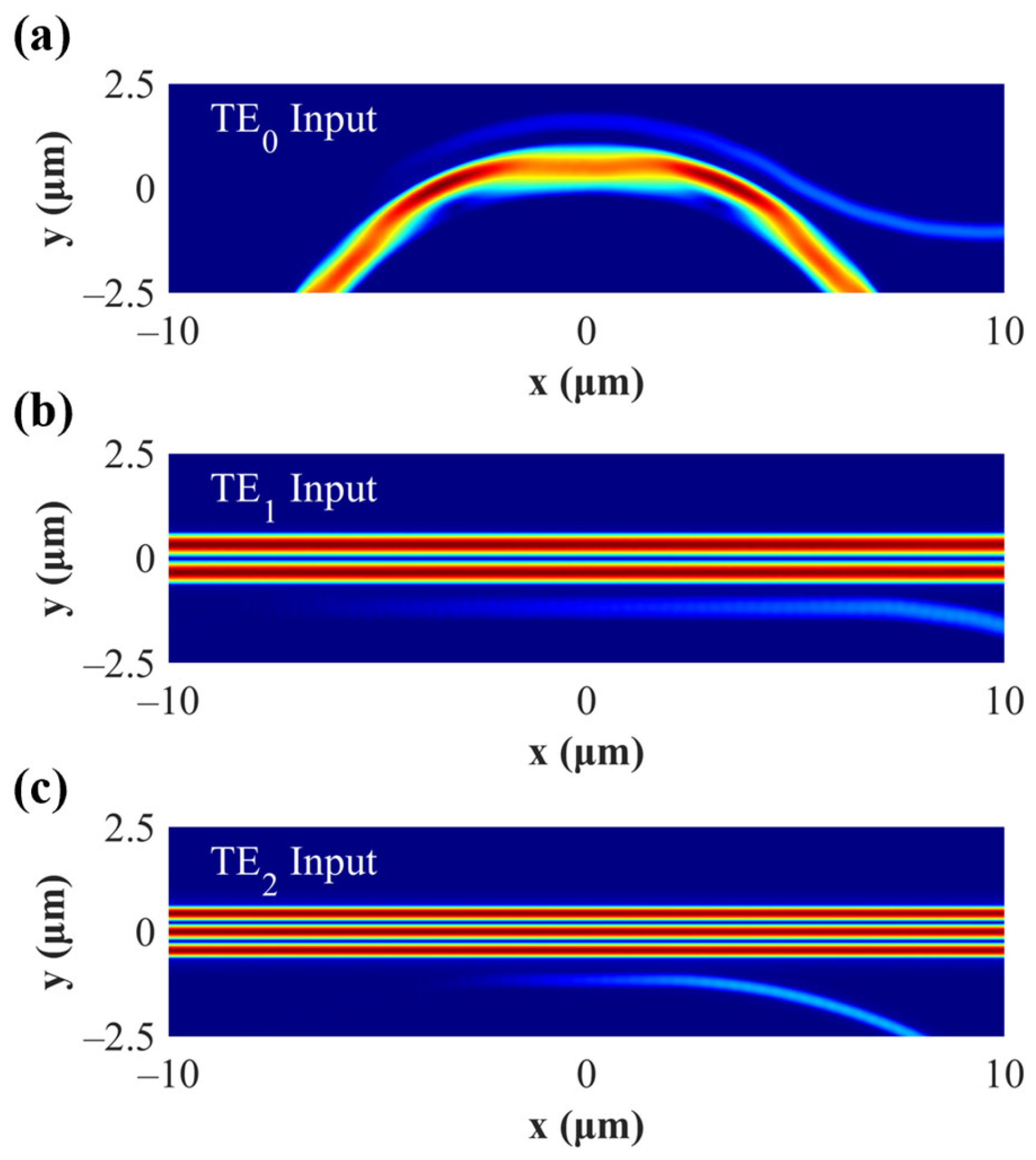
2.1. The Design of Multimode Waveguide Bend (MWB)

Conventional MWBs usually require a very large bending radius to avoid undesired losses and inter-mode crosstalk due to mode mismatch [30,35]. The performance of a MWB is strongly dependent on its shape, and several different special mathematical curves have been employed to optimize the MWB [36,37,38]. Among them, the cubic spline interpolation curves possess a high degree of freedom and are not limited by the well-defined curve functions [38]. For a given set of n data points ( x i , y i ) that follow x 1 <   x 2   <     <   x n , a smooth curve can be obtained by cubic spline interpolation, in which the adjacent data points are fitted by a cubic polynomial:
S i ( x ) = y i + b i ( x x i ) + c i ( x x i ) 2 + d i ( x x i ) 3 ,       x i x x i + 1 .
where i = 1, 2, …, n1, S i ( x ) is the ith spline curve, b i , c i , and d i are unknown coefficients. Cubic spline curves require the segments to be continuous at the nodes, and the first-order and second-order derivatives to be continuous at the nodes, which can be expressed as follows:
y i = S i 1 ( x i ) , i = 2 , 3 , , n . S i ( x i + 1 ) = S i + 1 ( x i + 1 ) , i = 1 , 2 , , n 2 . S i ( x i + 1 ) = S i + 1 ( x i + 1 ) , i = 1 , 2 , , n 2 .
the total number of unknown coefficients is 3n − 3 from Equation (1), while only 3n − 5 equations can be formulated according to Equation (2). Thus, it is often necessary to impose additional boundary conditions at the start and end points of the spline curve in practical applications. A commonly employed natural boundary condition can be formulated as follows [38]:
S 1 ( x 1 ) = 0 , S n 1 ( x n ) = 0 .
by combining Equation (1) to Equation (3), we can solve all the undetermined coefficients.
As shown in Figure 1a, to balance the trade-off between device size and performance, we choose the effective radius of the MWB as 8 μm. The width of both ends of the MWB is 1.3 μm, consistent with the straight multimode waveguide, supporting the first three-order TE modes. The MWB consists of two identical 45-degree curved sections, with its boundary outlined by two sets of cubic spline interpolation points, which are marked as blue circles. To obtain accurate device performance and smooth curve shapes, we choose 20 and 15 interpolation points in the inner and outer curves of the MWB. The optimization of this MWB by using traditional parameter scanning methods requires a large amount of computational resources and time. Therefore, we employ the adjoint method to optimize the dataset, which is significantly efficient for the inverse design of complex electromagnetic components [39,40]. By calculating the gradient of figure-of-merit (FOM) through only two simulations in each iteration, namely, forward and adjoint simulations, the adjoint method can significantly accelerate the optimization process.
The FOM is defined as mode overlap (η) between the input mode and the corresponding output mode of the MWB, similar to formulations in [35,41], and is easy to implement in Lumerical softwares from Ansys Canada Ltd. (Canonsburg, PA, Canada) The total FOM can be written as follows:
FOM = i = 0 2 FOM i = i = 0 2 η i
where i denotes the ith mode. A 1/4 ring waveguide with a radius of 8 μm and a width of 1.3 μm is chosen as the initial structure, and the interpolation points are uniformly distributed. Aided by the shape optimization within the Lumopt module of Ansys Lumerical, the 3D finite-difference time-domain (FDTD) solver is selected to maximize the FOM, and the L-BFGS-B algorithm is used to update the parameters [42]. The structure of the optimized MWB approximates a 1/4 circle that is wider at both ends and narrower in the middle. Figure 2 illustrates the optical field distributions of the three modes through the MWB and the corresponding insertion loss and crosstalk curves. There is no significant mode mismatch between the input and output waveguide ports. Moreover, within the wavelength range of 1.5 to 1.6 μm, the average losses for the TE0, TE1, and TE2 modes are 0.01 dB, 0.03 dB, and 0.03 dB, and the crosstalks are below −21.3 dB, −17.9 dB, and −17.3 dB, respectively.

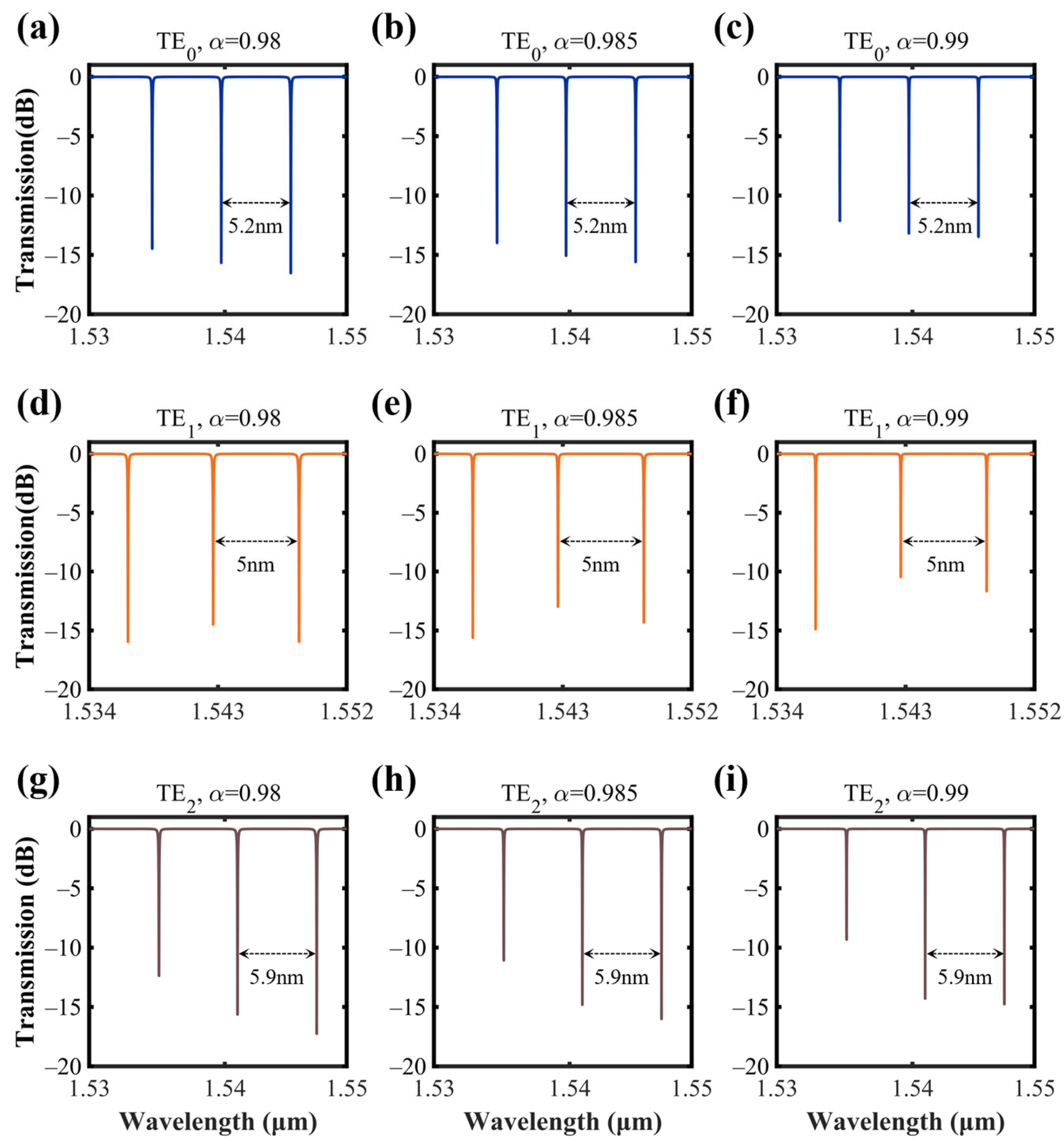
2.2. The Design of Multimode Micro-Racetrack Resonator (MMRR)

The proposed MMRR consists of a multimode micro-racetrack located at the center and three ADCs positioned at the periphery, as shown in Figure 1b. According to the coupled mode theory [43], when two waveguides are close enough, there will be periodic energy exchange between them via the evanescent fields. The employed ADC consists of a single-mode waveguide and a multimode waveguide, which enables mode conversion between a fundamental mode and a high-order mode. To achieve efficient mode conversions, the three coupling regions should be designed carefully, including widths of access waveguides, coupling lengths, and gaps between waveguides, as shown in Figure 3.
Figure 4a shows the effective indices of the first three-order modes in the waveguides with different widths at the wavelength of 1.55 μm, calculated by the finite difference eigenmode method. For the TE1 and TE2 modes, n eff 1 = n eff 2 should be fulfilled according to the phase-matching condition, where n eff 1 is the effective indices for the TE0 modes of the two access waveguides, and n eff 2 is the effective indices for the TE1 or TE2 modes of the multimode waveguide. Based on this principle, we choose the widths of the access waveguides ( W 2 and W 3 ) as 0.64 μm and 0.41 μm, respectively. Moreover, a bending ADC is used to couple the TE0 mode of the narrow access waveguide into the TE0 mode of the MWB. Similarly, n eff 1 R 1 = n eff 2 R 2 should be fulfilled according to the phase-matching condition [44], where R 1 and R 2 are the radii of curvature of the two bending waveguides. The width W 1 of the TE0 ADC can be calculated as 0.52 μm according to this formula.
Coupling lengths and gaps between waveguides affect the coupling coefficients of the MMRR, which determine the MMRR performance, like the IL and extinction ratio (ER). To make the MMRR suitable for integrated optoelectronic applications, a large FSR and ER are usually required. Thus, the expected FSR and ER of the MMRR are set to 5 nm and 20 dB. The FSR of an all-pass micro-racetrack resonator can be expressed as below:
FSR = λ c 2 n g L
where λ c = 1.55 μm, n g is the group refractive index of the mode, and L is the circumference of the multimode micro-racetrack. n g is defined as follows:
n g = n eff λ d n eff d λ
Figure 4b demonstrates the effective refractive index of each mode as a function of wavelength. It is fitted to a straight line using the least-squares method and the slope of the line to be brought into Equation (6) is derived to obtain the n g   of each mode. We first consider the TE1 mode in the multimode waveguide, which has a n g of 3.2325 at wavelength of 1.55 μm; so, the circumference L can be derived from Equation (5) as 148.65 μm under the target of an FSR of 5 nm.
To choose the coupling coefficients t of the three ADCs, we consider the relationship between the self-coupling coefficient and ER in the all-pass micro-racetrack resonator, which can be expressed as follows [45]:
ER = 20 log ( ( t + α ) ( 1 α t ) ( t α ) ( 1 + α t ) )
where α is the attenuation factor of the multimode micro-racetrack resonator. For the ring SOI waveguide with 5–10 μm bending radius, the loss is generally considered to be 5–20 dB/cm, which corresponds to an attenuation factor α of 0.98–0.99. Considering the inevitable fabrication errors, we analyzed three representative values of α, namely 0.98, 0.985, and 0.99, by which t can be calculated according to Equation (7).
Once the coupling coefficients t are clear, we can choose the appropriate coupling length by 3D FDTD simulations. To reduce the complexity of the device fabrication while simultaneously maintaining a compact device size, we selected the gaps of the three ADCs to be 200 nm, 200 nm, and 300 nm, respectively. Taking the case of α = 0.985 as an example, by carrying out 3D FDTD parameter scanning, we can derive the corresponding coupling region angle and the lengths of the three ADCs as 51.4 degrees, 10.57 μm, and 2.3 μm at the wavelength of 1.55 μm. Figure 5 illustrates the optical field distributions for the launched TE 0 , TE 1 , and TE2 modes in the three ADCs. In the TE0 ADC, the performance of the bending coupling is guaranteed due to the refractive index matching between the modes and the fact that the interpolation points at the outer boundary of the MWB are almost distributed along a conventional 1/4 bend. In the other two ADCs, the TE1 and TE2 modes injected from the bus multimode waveguide are coupled to the corresponding TE0 modes of the access waveguides as expected. No mode crosstalk is observed in each ADC.
Some of the design parameters for the three ADCs of the MMRR are listed in Table 1, in which α is a dimensionless parameter. In addition, other parameters can be summarized as follows: W 1 = 0.52 μm, W 2 = 0.64 μm, W 3 = 0.41 μm, W bus = 1.3 μm, G 1 = 0.2 μm, G 2 = 0.2 μm, G 3 = 0.3 μm.
We also calculated the coupling coefficient t at different wavelengths when the above parameters are employed, using the 3D FDTD solver. As illustrated in Figure 6, in the wavelength range of 1.5 to 1.6 μm, t is higher than 0.97 and increases with α. Since the coupling coefficient t is no longer linearly related to the wavelength, we can use polynomial fitting to derive the corresponding mathematical expression.
The transmission spectra of the three modes in the MMRR are then calculated. The relationship between transmission efficiency (T) and the wavelength of an all-pass micro-racetrack resonator can be expressed as follows [45]:
T = 10 log ( α 2 + t 2 2 α t cos θ 1 + α 2 t 2 2 α t cos θ )
where θ = 2 π n eff L / λ , which is the phase of the optical wave after propagating one complete round trip in the micro-racetrack resonator. Simultaneously considering the dispersion characteristics of n eff and t, shown in Figure 4b and Figure 6, the theoretical transmission spectrum for each mode can be calculated according to Equation (8).
As shown in Figure 7, under these different α, the FSRs of the three modes are 5.2 nm, 5 nm, and 5.9 nm, respectively. Here, we need to point out that since we first determine the circumference of the MMRR based on the n g   of the TE 1 mode with (5), and this value will not be changed for a determined MMRR, this leads to a slight difference in the FSR due to the n g distinction of the three modes.

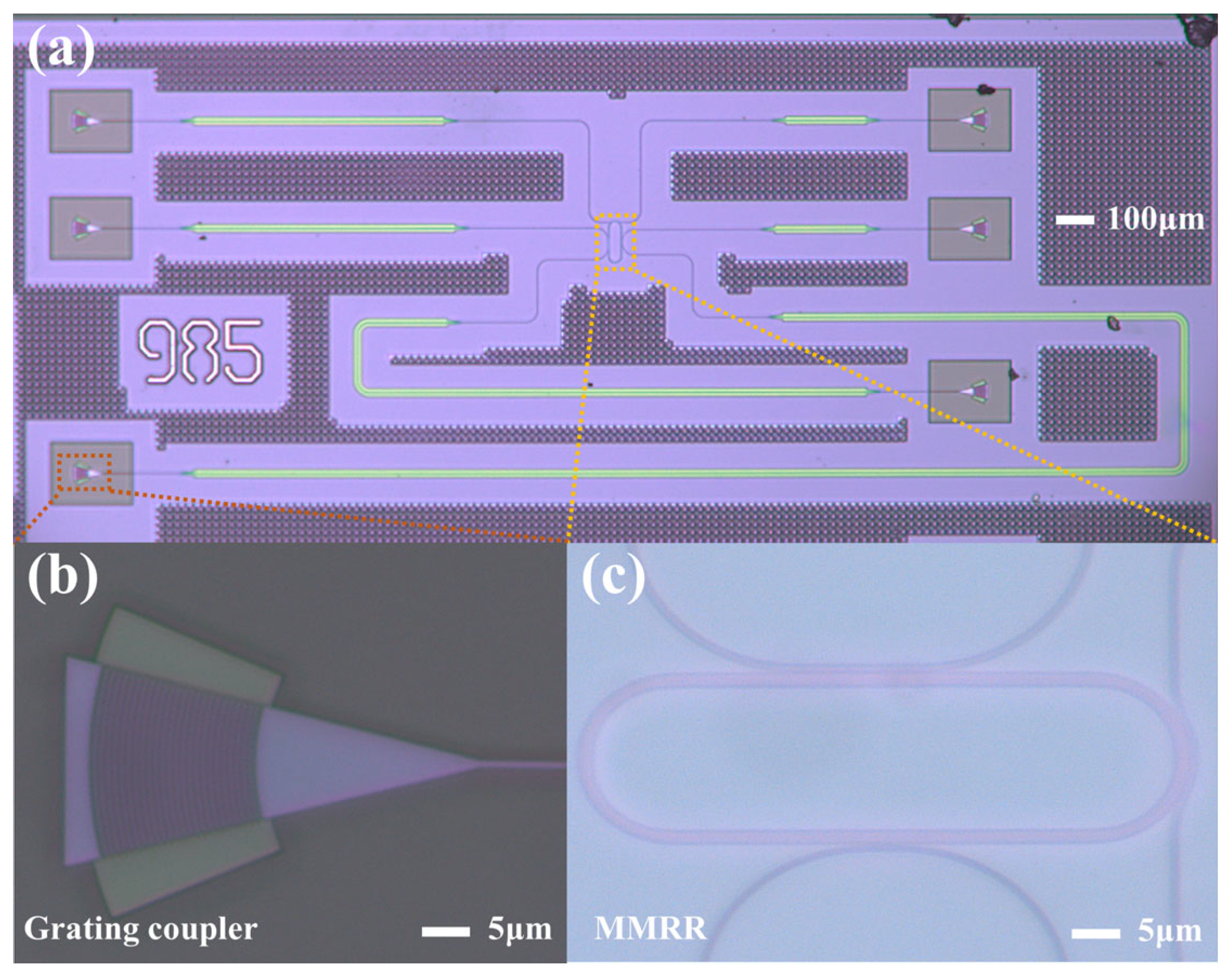
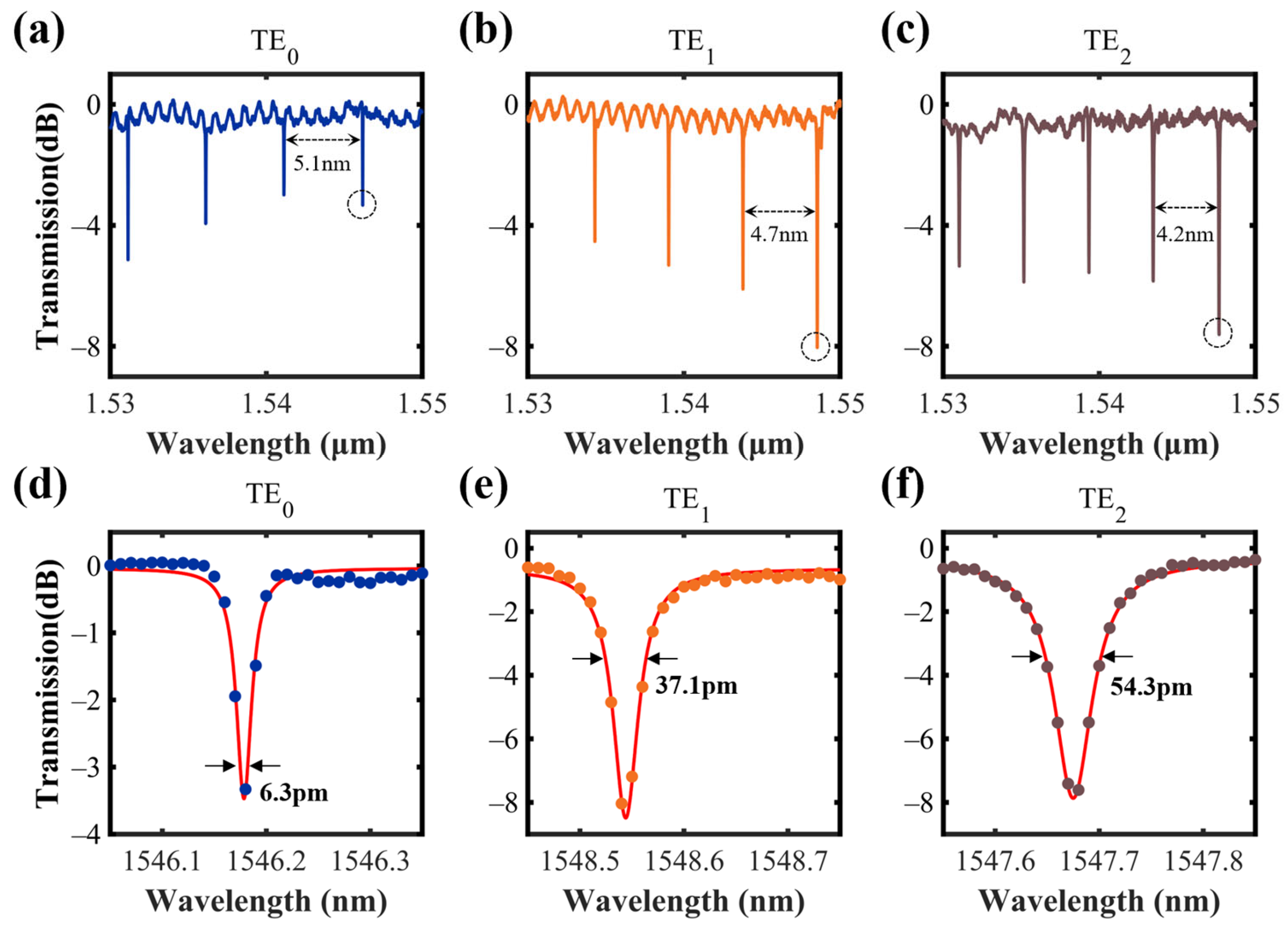
3. Fabrication and Characterization

Using a 193 nm dry lithography process, the designed MMRRs were fabricated on a 220 nm-thick SOI wafer with a 3 μm-thick silicon dioxide buried layer at Advanced Micro Foundry, Singapore. Figure 8 presents the microscope image of the devices, with clear boundaries and smooth contours shown in the etched MMRR. The footprint of the MMRR is only ~19 × 55 μm2, and six identical grating couplers are used for optical transmission between the device and the single-mode fibers.
An amplified spontaneous emission (ASE) source and an optical spectrum analyzer (OSA) are used to measure the transmission spectra of each mode in the fabricated MMRR. The ASE has a flat spectrum to support the measurement. To accurately characterize the spectra, the wavelength resolution of OSA is set to be 10 pm. The grating coupler is calibrated to obtain the best tilt angle and the lowest transmission loss. The transmission spectrum of the reference waveguide without the presence of the multimode micro-racetrack resonator is measured first for normalization. The real transmission spectra of each mode in MMRR are then obtained by subtracting the reference one, as shown in Figure 9a–c. In addition, the tilt angle of the grating couplers should remain constant during the measurement. Here, the spectra are only shown in a 20 nm range for better observation of the FSRs. All three modes in the MMRR exhibit ILs below −1 dB in the measured wavelength range. Additionally, the transmission spectra of each mode contain only one set of uniformly distributed resonance peaks, suggesting that the crosstalk between modes is negligible.
We select the resonant peaks near 1546.18 nm, 1548.55 nm, and 1547.67 nm for the three modes to analyze the loaded Q factors of the MMRR, and utilize Lorentzian curves to fit the measured data, as shown in Figure 9d–f. The full widths at half-maximum are 6.3 pm, 37.1 pm, and 54.3 pm for TE0, TE1, and TE2 modes, corresponding to the calculated loaded Q factors of 2.3 × 10⁵, 4.1 × 10⁴, and 2.9 × 10⁴, respectively. Moreover, the FSRs for the TE0 and TE1 modes are 5.1 nm and 4.7 nm, which are close to the calculated values. The FSR for the TE2 mode is 4.2 nm, with a larger difference to the calculated value. This may come from the fact that the coupling length of TE2 ADC is the smallest, so it is most susceptible to process errors. Nonetheless, the fabricated MMRR still exhibits a sufficiently large FSR in all three modes, which is highly advantageous for applications, such as wavelength division multiplexing, optical sensing, and microwave photonics.

4. Discussions

4.1. Performance Comparison

Table 2 summarizes and compares the performances of the reported MMRRs. It is evident that our MMRR exhibits the smallest effective radius. Furthermore, the fabrication of our MMRR only requires a single-step lithography and etching step. This suggests that our device is suitable for low-cost, large-scale production.

4.2. Loaded Q Factor

The loaded Q factor Qload is inversely proportional to the total energy loss of the resonator and can be divided into two parts, internal loss (corresponding to Qint) and coupling loss (corresponding to Qcoup). Therefore, the following applies:
1 Q load = 1 Q int + 1 Q coup
following the calculation method shown in Figure 9, we analyze Qint of the MMRR for the three modes. The resonant wavelengths are selected as 1544.87 nm, 1548.66 nm, and 1546.78 nm from the transmission spectra in Figure 7. The full widths at half-maximum are calculated as 5.9 pm, 34 pm, and 44.1 pm for TE0, TE1, and TE2 modes, corresponding to Qint of 2.6 × 10⁵, 4.6 × 10⁴, and 3.5 × 10⁴, respectively. Equation (9) indicates two methods to increase loaded Qload: (1) Decrease internal loss, which requires a high-quality SOI wafer. (2) Reduce coupling loss, which requires advanced lithography technology.

4.3. Fabrication Errors

The FSR of the TE2 mode for the fabricated MMRR is 4.2 nm which deviates from the theoretical value (5.9 nm). It may be due to the following: (1) The field distribution of the TE2 mode overlaps with the sidewall of the waveguide. The sidewall is relatively rough and changes the propagation performance of the TE2 mode. (2) The parameters of the MMRR, such as waveguide widths, waveguides thicknesses, and waveguide sidewall angles, may also deviate from the designed value, which causes the error between the theoretical and experimental FSR. (3) The bus waveguide width Wbus is related to the group refractive index ng and the FSR of the TE2 mode.

5. Conclusions

In summary, we proposed and experimentally demonstrated a compact MMRR on a commercial 220 nm SOI platform, which is composed of shape-optimized MWBs and ADCs. Two cubic spline curves were chosen to define the MWB and the adjoint methods were used for optimization, achieving an effective radius of 8 μm. Three ADCs were carefully designed according to the phase-matching condition and the desired transmission performance. The fabricated MMRR exhibits high loaded Q factors of 2.9 × 10⁴ to 2.3 × 10⁵ and large FSRs of 4.2 to 5.1 nm for TE 0 , TE 1 , and TE 2 modes. The device footprint is only ~19 × 55 μm2, making it highly suitable for integrated optoelectronic applications. This work demonstrates the potential of ultra-compact MMRRs for high-density integration into next-generation optical communication systems and microwave photonics. The proposed MMRR can be applied to various multimode applications, such as MDM systems, microwave photonic filters, and nonlinear optics. In addition, some improvements could be introduced in future works, such as more flexible mathematical curves, different optimization methods, and other material platforms.

Author Contributions

Conceptualization, Z.L. and C.C.; methodology, Z.L. and C.C.; software, C.C.; validation, Z.L. and C.C.; formal analysis, C.C.; investigation, Z.L.; resources, Z.L.; data curation, C.C.; writing—original draft preparation, Z.L.; writing—review and editing, Z.L. and C.C.; visualization, Z.L. and C.C.; supervision, L.Y.; project administration, X.F. and L.Y.; funding acquisition, X.F. and L.Y. All authors have read and agreed to the published version of the manuscript.

Funding

This research received no external funding.

Institutional Review Board Statement

Not applicable.

Informed Consent Statement

Not applicable.

Data Availability Statement

Relevant data are available from the authors upon reasonable request.

Conflicts of Interest

The authors declare no conflicts of interest.

Abbreviations

The following abbreviations are used in this manuscript:
MMRRmultimode micro-racetrack resonator
MWBmultimode waveguide bend
ADCasymmetric directional coupler
FSRfree spectral range
MDMmode division multiplexing
SWGsubwavelength grating
ILinsertion loss
TIRtotal internal reflection
SOIsilicon-on-insulator
FOMfigure-of-merit
FDTDfinite-difference time-domain
ERextinction ratio
EBLelectron beam lithography
LNOIlithium-niobate-on-insulator
AlGaAsOIAlGaAs-on-insulator
MSMMRmultiple single mode micro-racetracks
OSAoptical spectrum analyzer
ASEamplified spontaneous emission
TOtransformation optics

References

  1. Yao, J.; Capmany, J. Microwave Photonics. Sci. China Inf. Sci. 2022, 65, 221401. [Google Scholar] [CrossRef]
  2. Marpaung, D.; Yao, J.; Capmany, J. Integrated Microwave Photonics. Nat. Photon. 2019, 13, 80–90. [Google Scholar] [CrossRef]
  3. Eppenberger, M.; Messner, A.; Bitachon, B.I.; Heni, W.; Blatter, T.; Habegger, P.; Destraz, M.; De Leo, E.; Meier, N.; Del Medico, N.; et al. Resonant Plasmonic Micro-Racetrack Modulators with High Bandwidth and High Temperature Tolerance. Nat. Photon. 2023, 17, 360–367. [Google Scholar] [CrossRef]
  4. Kashi, A.A.; Van Der Tol, J.J.G.M.; Lebby, M.S.; Zhang, X.; Williams, K.; Jiao, Y. Ring-Assisted Mach-Zehnder Modulator on the InP Membrane on Silicon Platform. J. Light. Technol. 2024, 42, 4553–4562. [Google Scholar] [CrossRef]
  5. Green, W.M.J.; Lee, R.K.; DeRose, G.A.; Scherer, A.; Yariv, A. Hybrid InGaAsP-InP Mach-Zehnder Racetrack Resonator for Thermooptic Switching and Coupling Control. Opt. Express 2005, 13, 1651–1659. [Google Scholar] [CrossRef]
  6. Xu, H.-H.; Huang, Q.-Z.; Li, Y.-T.; Yu, Y.-D.; Yu, J.-Z. Sub-Nanosecond Optical Switch Based on Silicon Racetrack Resonator. Chin. Phys. B 2010, 19, 084210. [Google Scholar] [CrossRef]
  7. Tao, Z.; Tao, Y.; Jin, M.; Qin, J.; Chen, R.; Shen, B.; Wu, Y.; Shu, H.; Yu, S.; Wang, X. Highly Reconfigurable Silicon Integrated Microwave Photonic Filter towards Next-Generation Wireless Communication. Photon. Res. 2023, 11, 682. [Google Scholar] [CrossRef]
  8. Yan, H.; Xie, Y.; Zhang, L.; Dai, D. Wideband-Tunable on-Chip Microwave Photonic Filter with Ultrahigh-Q U-Bend-Mach–Zehnder-Interferometer-Coupled Microring Resonators. Laser Photonics Rev. 2023, 17, 2300347. [Google Scholar] [CrossRef]
  9. Zhao, W.; Peng, Y.; Cao, X.; Zhao, S.; Liu, R.; Wei, Y.; Liu, D.; Yi, X.; Han, S.; Wan, Y.; et al. 96-Channel on-Chip Reconfigurable Optical Add-Drop Multiplexer for Multidimensional Multiplexing Systems. Nanophotonics 2022, 11, 4299–4313. [Google Scholar] [CrossRef]
  10. James, A.; Novick, A.; Rizzo, A.; Parsons, R.; Jang, K.; Hattink, M.; Bergman, K. Scaling Comb-Driven Resonator-Based DWDM Silicon Photonic Links to Multi-Tb/s in the Multi-FSR Regime. Optica 2023, 10, 832. [Google Scholar] [CrossRef]
  11. Yi, X.; Zhao, W.; Li, C.; Zhang, L.; Xiang, Y.; Liu, C.; Shi, Y.; Liu, L.; Dai, D. Reconfigurable Optical Add-Drop Multiplexers for Hybrid Mode-/Wavelength-Division-Multiplexing Systems. Adv. Photon. Nexus 2023, 2, 066004. [Google Scholar] [CrossRef]
  12. Mojaver, K.R.; Safaee, S.M.R.; Morrison, S.S.; Liboiron-Ladouceur, O. Recent Advancements in Mode Division Multiplexing for Communication and Computation in Silicon Photonics. J. Light. Technol. 2024, 42, 7860–7870. [Google Scholar] [CrossRef]
  13. Li, C.; Liu, D.; Dai, D. Multimode Silicon Photonics. Nanophotonics 2019, 8, 227–247. [Google Scholar] [CrossRef]
  14. Wu, X.; Huang, C.; Xu, K.; Shu, C.; Tsang, H.K. Mode-Division Multiplexing for Silicon Photonic Network-on-Chip. J. Light. Technol. 2017, 35, 3223–3228. [Google Scholar] [CrossRef]
  15. Dai, D.; Li, C.; Wang, S.; Wu, H.; Shi, Y.; Wu, Z.; Gao, S.; Dai, T.; Yu, H.; Tsang, H. 10-Channel Mode (de)Multiplexer with Dual Polarizations. Laser Photonics Rev. 2018, 12, 1700109. [Google Scholar] [CrossRef]
  16. Zhao, W.; Yi, X.; Peng, Y.; Zhang, L.; Chen, H.; Dai, D. Silicon Multimode Waveguide Crossing Based on Anisotropic Subwavelength Gratings. Laser Photonics Rev. 2022, 16, 2100623. [Google Scholar] [CrossRef]
  17. Chang, W.; Zhang, M. Silicon-Based Multimode Waveguide Crossings. J. Phys. Photonics 2020, 2, 022002. [Google Scholar] [CrossRef]
  18. Liu, R.; Lu, L.; Zhang, P.; Chang, W.; Liu, D.; Zhang, M. Integrated Dual-Mode 3-dB Power Splitter Based on Multimode Interference Coupler. IEEE Photon. Technol. Lett. 2020, 32, 883–886. [Google Scholar] [CrossRef]
  19. Sun, S.; Fu, Y.; Li, S.; Ning, X.; Zhou, Z.; Zhang, D.; Wang, X. Ultra-Broadband Multimode Fiber-to-Chip Edge Coupler Based on Periodically Segmented Waveguides. Opt. Lett. 2024, 49, 6061. [Google Scholar] [CrossRef]
  20. Zhang, R.; Li, X.; He, Y.; Chen, G.; Xiong, L.; Chen, H.; Fontaine, N.K.; Zhang, Y.; Xie, W.; Su, Y. Ultra-High Bandwidth Density and Power Efficiency Chip-To-Chip Multimode Transmission through a Rectangular Core Few-Mode Fiber. Laser Photonics Rev. 2023, 17, 2200750. [Google Scholar] [CrossRef]
  21. Dai, D.; Bowers, J.E. Silicon-Based on-Chip Multiplexing Technologies and Devices for Peta-Bit Optical Interconnects. Nanophotonics 2014, 3, 283–311. [Google Scholar] [CrossRef]
  22. Jiang, X.; Wu, H.; Dai, D. Low-Loss and Low-Crosstalk Multimode Waveguide Bend on Silicon. Opt. Express 2018, 26, 17680–17689. [Google Scholar] [CrossRef] [PubMed]
  23. Sun, C.; Yu, Y.; Chen, G.; Zhang, X. Ultra-Compact Bent Multimode Silicon Waveguide with Ultralow Inter-Mode Crosstalk. Opt. Lett. 2017, 42, 3004. [Google Scholar] [CrossRef] [PubMed]
  24. Wu, H.; Li, C.; Song, L.; Tsang, H.-K.; Bowers, J.E.; Dai, D. Ultra-Sharp Multimode Waveguide Bends with Subwavelength Gratings. Laser Photonics Rev. 2019, 13, 1800119. [Google Scholar] [CrossRef]
  25. Li, W.; Chen, J.; Zhu, M.; Dai, D.; Shi, Y. Ultra-Compact Multimode Waveguide Bend With Optimized Dual Bezier Contours. IEEE Photon. Technol. Lett. 2023, 35, 1131–1134. [Google Scholar] [CrossRef]
  26. Li, S.; Cai, L.; Gao, D.; Dong, J.; Hou, J.; Yang, C.; Chen, S.; Zhang, X. Compact and Broadband Multimode Waveguide Bend by Shape-Optimizing with Transformation Optics. Photon. Res. 2020, 8, 1843. [Google Scholar] [CrossRef]
  27. Sun, S.; Dong, P.; Zhang, F.; Wang, J.; Zhu, N.; Shi, Y. Inverse Design of Ultra-Compact Multimode Waveguide Bends Based on the Free-Form Curves. Laser Photonics Rev. 2021, 15, 2100162. [Google Scholar] [CrossRef]
  28. Sun, S.; Yang, Z.; Wang, J.; Zhang, R.; Zhang, F.; Zhu, N.; Wan, L.; Li, Z. Ultra-Sharp Silicon Multimode Waveguide Bends Based on Double Free-Form Curves. Photonics Res. PRJ 2022, 10, 1484–1490. [Google Scholar] [CrossRef]
  29. Tan, J.; Xiao, H.; Ma, M.; Zhou, X.; Yuan, M.; Dubey, A.; Boes, A.; Nguyen, T.G.; Ren, G.; Su, Y.; et al. Arbitrary Access to Optical Carriers in Silicon Photonic Mode/Wavelength Hybrid Division Multiplexing Circuits. Opt. Lett. 2022, 47, 3531. [Google Scholar] [CrossRef]
  30. Cai, L.; Gao, D.; Dong, J.; Hou, J.; Yang, C.; Chen, S.; Zhang, X. Compact and High Q-Factor Multimode Racetrack Ring Resonator Based on Transformation Optics. Opt. Express 2022, 30, 15766. [Google Scholar] [CrossRef]
  31. Chen, Z.; Ye, M.; Zhang, L.; Zhang, Q. Compact mode-insensitive ring resonator based on SWG coupler and Euler bends. In Proceedings of the AOPC 2021: Micro-Optics and MOEMS, Beijing, China, 20–22 June 2021; Volume 12066, pp. 144–149. [Google Scholar]
  32. Wei, C.; Li, J.; Jia, Q.; Li, D.; Liu, J. Ultrahigh-Q Lithium Niobate Microring Resonator with Multimode Waveguide. Opt. Lett. 2023, 48, 2465. [Google Scholar] [CrossRef] [PubMed]
  33. Ye, C.; Liu, Y.; Zhou, Y.; Zhao, Y.; Zheng, Y.; Kim, C.; Oxenløwe, L.K.; Yvind, K.; Pu, M. Multimode AlGaAs-on-Insulator Microring Resonators for Nonlinear Photonics. IEEE J. Sel. Top. Quantum Electron. 2024, 30, 1–11. [Google Scholar] [CrossRef]
  34. Ye, M.; Sun, C.; Yu, Y.; Ding, Y.; Zhang, X. Silicon Integrated Multi-Mode Ring Resonator. Nanophotonics 2021, 10, 1265–1272. [Google Scholar] [CrossRef]
  35. Yang, S.; Jia, H.; Niu, J.; Fu, X.; Yang, L. CMOS-Compatible Ultra-Compact Silicon Multimode Waveguide Bend Based on Inverse Design Method. Opt. Commun. 2022, 523, 128733. [Google Scholar] [CrossRef]
  36. Dou, T.; Yue, S.; Hou, Y.; Wang, R.; Shi, H.; Li, Y.; Feng, Y.; Zhang, Z. Ultra-Sharp Multimode Waveguide Bends Based on Superellipse Curves and Shallowly Etched Nanoslots Designed by an Intelligent Algorithm. J. Light. Technol. 2024, 42, 5249–5261. [Google Scholar] [CrossRef]
  37. Liao, J.; Tian, Y.; Yang, Z.; Xu, H.; Dai, T.; Zhang, X.; Kang, Z. Broadband and Compact Silicon Multimode Waveguide Bends Based on Hybrid Shape Optimization. J. Light. Technol. 2024, 42, 4882–4891. [Google Scholar] [CrossRef]
  38. Zhang, E.; Yang, S.; Zhang, L. General Waveguide Bend Design Based on Cubic Spline Interpolation and Inverse Design. J. Light. Technol. 2024, 42, 4614–4625. [Google Scholar] [CrossRef]
  39. Lalau-Keraly, C.M.; Bhargava, S.; Miller, O.D.; Yablonovitch, E. Adjoint Shape Optimization Applied to Electromagnetic Design. Opt. Express 2013, 21, 21693. [Google Scholar] [CrossRef]
  40. Georgieva, N.K.; Glavic, S.; Bakr, M.H.; Bandler, J.W. Feasible Adjoint Sensitivity Technique for EM Design Optimization. IEEE Trans. Microw. Theory Tech. 2002, 50, 2751–2758. [Google Scholar] [CrossRef]
  41. Cheng, C.; Yang, S.; Liu, W.; Liu, S.; Huo, Y.; Fu, X.; Yang, L. Ultra-Compact Inverse Designed Multimode Waveguide Bend Based on Levelset Method. IEEE Photonics Technol. Lett. 2024, 36, 571–574. [Google Scholar] [CrossRef]
  42. Teytaud, O.; Bennet, P.; Moreau, A. Discrete Global Optimization Algorithms for the Inverse Design of Silicon Photonics Devices. Photonics Nanostruct.-Fundam. Appl. 2022, 52, 101072. [Google Scholar] [CrossRef]
  43. Haus, H.A.; Huang, W. Coupled-Mode Theory. Proc. IEEE 1991, 79, 1505–1518. [Google Scholar] [CrossRef]
  44. Dai, D.; Bowers, J.E. Novel Ultra-Short and Ultra-Broadband Polarization Beam Splitter Based on a Bent Directional Coupler. Opt. Express 2011, 19, 18614–18620. [Google Scholar] [CrossRef]
  45. McKinnon, W.R.; Xu, D.X.; Storey, C.; Post, E.; Densmore, A.; Delâge, A.; Waldron, P.; Schmid, J.H.; Janz, S. Extracting Coupling and Loss Coefficients from a Ring Resonator. Opt. Express 2009, 17, 18971. [Google Scholar] [CrossRef]
Figure 1. (a) Schematic of the MWB with an effective radius of 8 μm and a waveguide width of 1.3 μm. The control points of the cubic spline curve are denoted as blue circles. (b) Diagram of the proposed MMRR. The TE0, TE1, and TE2 ADCs are highlighted by the black dashed box.
Photonics 12 00326 g001
Figure 2. The z component of the magnetic field Hz distribution and transmission spectra for (a,b) TE0, (c,d) TE1, and (e,f) TE2 modes. The average insertion losses for three modes are 0.01 dB, 0.03 dB, and 0.03 dB, respectively. The maximum crosstalk for TE0, TE1, and TE2 modes are −21.3 dB, −17.9 dB, and −17.3 dB, respectively.
Photonics 12 00326 g002
Figure 3. (a) Detailed schematic for bend coupling region of TE0 ADC; the outer boundary of the MWB is set to 1/4 arc to guarantee the performance. Diagram of straight coupling region for (b) TE1 ADC (c) TE2 ADC; these parameters are chosen carefully to obtain the desired low crosstalk and transmission coefficient.
Photonics 12 00326 g003
Figure 4. Effective indices of TE0, TE1, and TE2 modes for different (a) widths (for the calculation of W2 and W3 which are denoted as green and red) and (b) wavelengths (for the calculation of the group refractive index).
Photonics 12 00326 g004
Figure 5. (a) TE0 ADC, (b) TE1 ADC, and (c) TE2 ADC electric field distributions for the MMRR at 1.55 μm.
Photonics 12 00326 g005
Figure 6. The relationship between coupling coefficient and wavelength for (a) TE0 ADC, (b) TE1 ADC, and (c) TE2 ADC under different attenuation factors.
Photonics 12 00326 g006
Figure 7. Transmission spectra of the MMRR for different attenuation factors and modes.
Photonics 12 00326 g007
Figure 8. Microscope images of the fabricated MMRR. (a) Overall picture for fabricated devices. (b) Grating coupler. (c) The zooming-in micrographs of MMRR.
Photonics 12 00326 g008
Figure 9. Transmission spectra of the fabricated MMRR. (ac) Transmission spectra for each mode. (df) The measured data (scattered dots) and Lorentzian fit curves (red lines) around resonant peaks for each mode.
Photonics 12 00326 g009
Table 1. Design parameters for three ADCs of the MMRR.
αθ (Degree) L 2 (μm) L 3 (μm)
0.9862.5712.743.27
0.98551.410.572.3
0.9942.868.031.28
Table 2. Comparison of the performance of our device with MMRRs proposed in recent years.
Ref.MethodRadius (μm)FSR (nm)Loaded QModesFabricationPlatform
[29]MSMMRRmax = 1000, Rmin = 30 *1.34\3 TEEBLSOI
[30]TO153.75.9 × 1043 TEEBLSOI
[31]SWGRmax = 600, Rmin = 10 *3.8\2 TE\SOI
[32]Euler curveRmax = 250, Rmin = 130 *0.454.1 × 1061 TEEBLLNOI
[33]Taper waveguide252.17.8 × 1052 TEEBLAlGaAsOI
[34]TIR\6.6573004 TEEBLSOI
This workCubic spline curve85.12.3 × 1053 TELithographySOI
* These bends are based on Euler curves with variant curvatures.
Disclaimer/Publisher’s Note: The statements, opinions and data contained in all publications are solely those of the individual author(s) and contributor(s) and not of MDPI and/or the editor(s). MDPI and/or the editor(s) disclaim responsibility for any injury to people or property resulting from any ideas, methods, instructions or products referred to in the content.

