1. Introduction
With the rapid development of the internet, cloud computing, artificial intelligence, and other technologies, the demand for photonic integrated circuits (PICs) has increased. Silicon-on-insulator (SOI) platforms are some of the most popular platforms for actualizing low-cost PICs due to their complementary metal–oxide–semiconductor (CMOS) compatibility. Simultaneously, the high refractive index contrast between the core and cladding gives SOI platforms the ability to implement high-density integration. However, the high-refractive-index contrast and significant difference between the width and height of typical SOI waveguides have also contributed to their strong polarization dependence. In addition, 2 × 2 3 dB couplers are some of the most critical components in PICs, and they are often used in Mach–Zehnder interferometers (MZIs) [
1] to split or combine light. MZIs are widely used in optical modulations [
2], switches [
3], optical computing [
4], microwave photonics (MPW) [
5,
6], etc. Therefore, realizing polarization-insensitive 2 × 2 3 dB couplers is essential for realizing various polarization-insensitive devices and systems. Polarization-independent 3 dB couplers have been implemented in many ways, including subwavelength-grating (SWG)-assisted couplers [
7], multimode interference (MMI) couplers [
8], bent directional couplers (DCs) [
9], and adiabatic couplers (ADCs) [
10,
11]. SWG-assisted couplers can achieve a broad bandwidth and low insertion loss (IL). Nevertheless, SWG-assisted couplers require the precise control of the shape and size of the periodic structure. MMI couplers with a broad bandwidth, small footprint, and low loss are only utilized as 1 × 2 power splitters. Bent DCs, which consist of a cascade of bent waveguides, also require a high fraction precision. ADCs operate based on the evolution of individual modes, resulting in a large bandwidth and high fabrication tolerance. However, to avoid the excitation of undesired modes, ADCs often have very long lengths. Therefore, the realization of broadband, low-loss, compact, and highly manufacturing-tolerant 2 × 2 3 dB couplers remain to be further explored.
Recently, inverse design has emerged as a powerful approach in photonics design for obtaining compact and high-performance devices [
12], such as grating couplers [
13], wavelength (de)multiplexers [
14], and mode (de)multiplexers [
15]. Shape optimization based on the adjoint method [
16] is a gradient-based algorithm, and the shape of the device is determined by a designer-specified curve. So far, there have been limited investigations into the utilization of adjoint shape optimization for the design of polarization-insensitive 3 dB couplers. B-spline curves [
17] have some advantages over Bézier curves, which have been used in shape optimization for many photonic devices [
18,
19]. Compared with Bézier curves, B-spline curves have more flexibility when the number of control points is very large, since the degree of the curve function is not necessarily equal to the number of control points minus one and a single control point no longer affects the shape of the whole curve. However, more control points mean more time is needed to compute the gradient. In addition, for B-spline curves, the number of control points, the order of the curves, and the distribution of the knots can all be freely chosen, meaning that more manual parameter adjustments are required. Therefore, in this study, we combine B-splines and adjoint shape optimization to calculate a large number of parameters quickly while utilizing the advantages of B-spline curves.
In this work, we propose and experimentally demonstrate a compact polarization-insensitive 2 × 2 3 dB quasi-adiabatic coupler using shape optimization based on the adjoint method and B-spline curves. During the optimization, we introduced the supermode of the two-waveguide system as the forward and adjoint sources to reduce the number of simulations needed for this multi-objective problem. In addition, we separately optimized the coupling region and the input region of the coupler. Our coupler has a mode coupling length of 12 μm and a minimum feature size of 150 nm. The numerical simulation resulted in an insert loss (IL) of less than 0.09 dB and a splitting ratio between 45% and 55% over a broad bandwidth of 140 nm for both the TE and TM polarizations. We fabricated the devices on the SOI platform. The experimental results show that the TM mode achieved a power splitting ratio within 3 ± 0.46 dB (50% ± 5%) over the wavelength range of 1525 nm–1600 nm, and the TE mode achieved the same power splitting ratio from 1576 nm to 1610 nm.
2. Design and Analysis
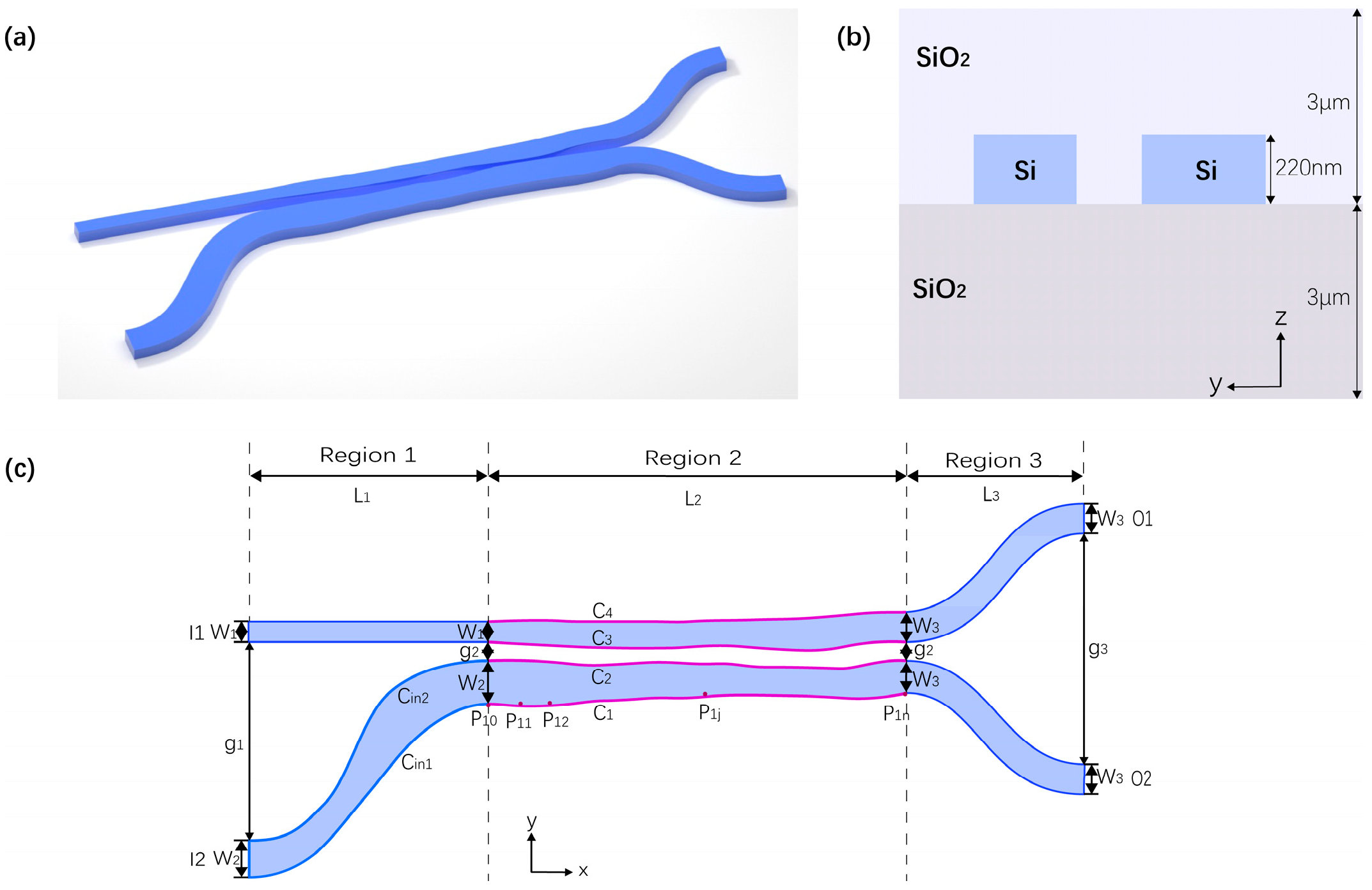
The schematic for our 2 × 2 3 dB coupler is shown in
Figure 1. The coupler is designed based on a 220 nm thick SOI platform with a 3 μm thick buried oxide layer and a 3 μm thick upper silica cladding layer.
Figure 1a,b show a three-dimensional view and a cross-sectional view of the coupler, respectively.
Figure 1c shows a top view of the coupler, showing that the device consists of three regions. In region 1, one straight waveguide and one S-shaped waveguide constitute the input section of the device. The widths of these two waveguides are W
1 = 350 nm and W
2 = 550 nm, and the gap between them gradually decreases from g1 = 1.65 μm to g2 = 150 nm over the length of L
1 = 30 μm. To make the device more compact, we optimized the shape of the standard S-shaped waveguide by two B-spline curves
. After optimization, the length of the input section was reduced to 15 μm. In region 2, a two-waveguide system constitutes the coupling section of the device and is also the most critical region of the design. In our design, the shape of these two waveguides is defined by four B-spline curves
, and the control points
of these curves are determined by shape-based optimization. The length of this section is L
2 = 12 um. In region 3, two symmetrical S-shaped waveguides with width W
3 = 450 nm and length L
3 = 10 μm separate the gap from g
2 = 150 nm to g
3 = 1.6 μm, forming the output section of the device.
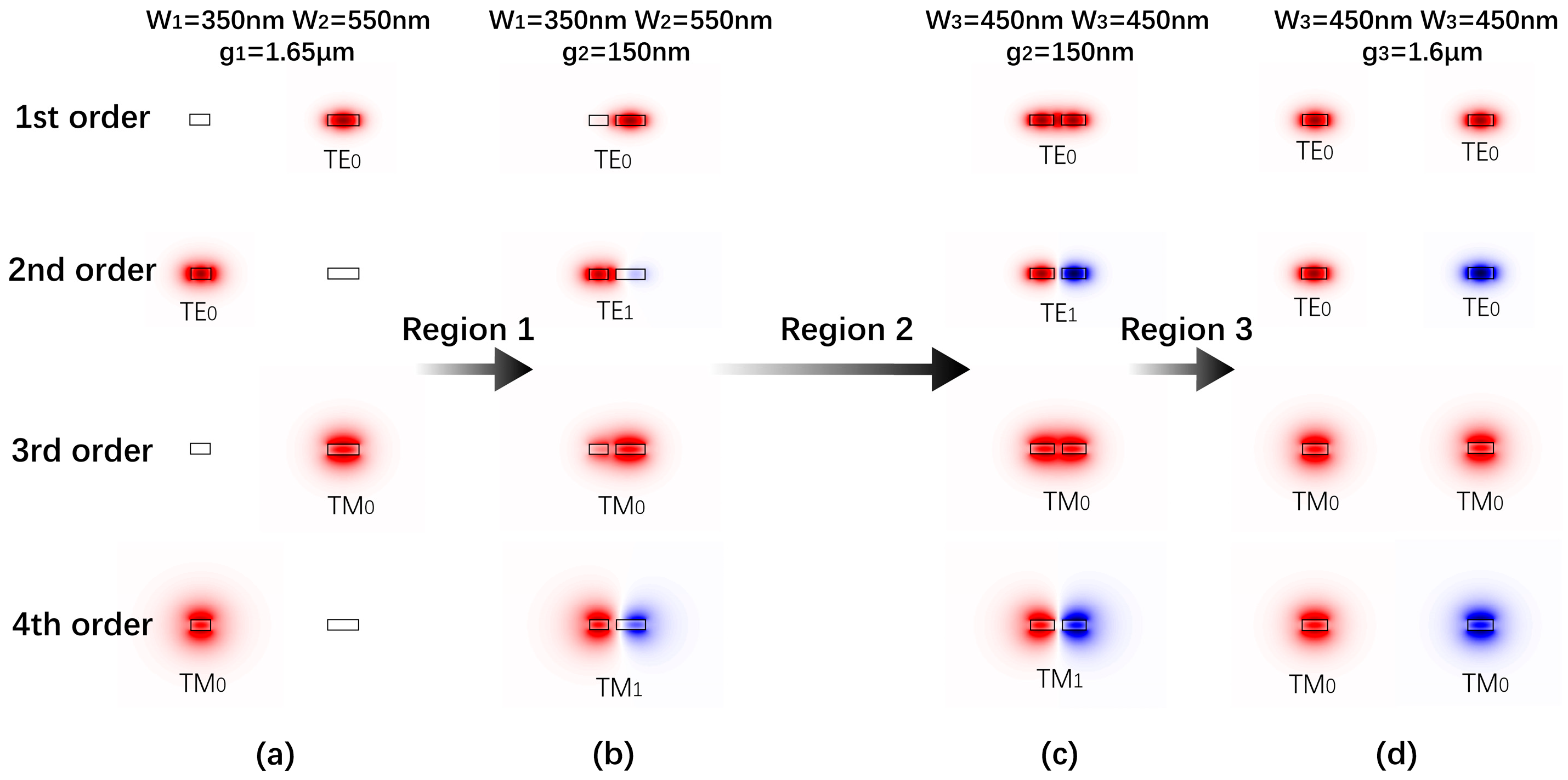
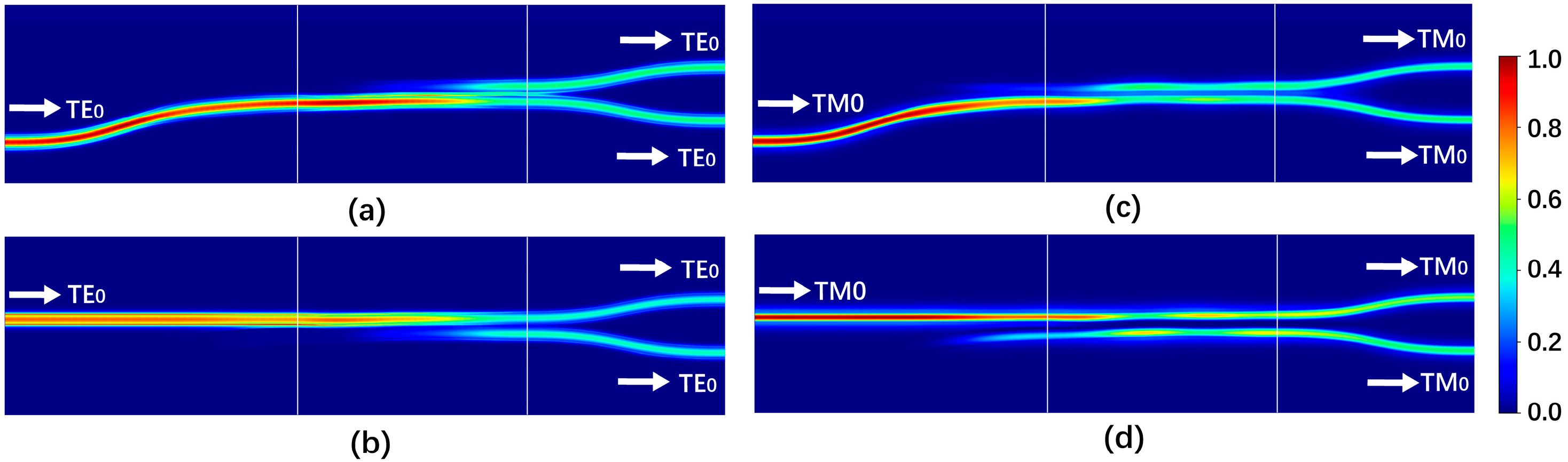
Figure 2 illustrates the mode profiles for each section’s input and output ports. In this paper, we order the modes of the two-waveguide system according to the effective index from largest to smallest. When TE
0-/TM
0-mode light is launched into input I1 on the narrow waveguide, the second-/fourth-order supermode of the two asymmetrical waveguides is initially excited in the coupling section and then evolves into the odd supermode of the two symmetrical waveguides. At the two outputs O1 and O2, the light is split evenly and has a π phase difference. Similarly, when TE
0-/TM
0-mode light is launched into input I2 on the wide waveguide, the first-/third order supermode of the two asymmetrical waveguides is excited and then evolves into the even supermode of the two symmetrical waveguides. At the two outputs O1 and O2, the light has the same intensity and phase.
ADCs usually require a long coupling region to avoid the input supermode coupling into the other unexpected supermode with the same polarization during its evolution toward the output port. We use an inverse design to shorten the evolution length while maintaining the adiabatic evolution of the excited supermodes along the coupling region. The expression of the four B-spline curves is:
where
represents the (
j+1)-th control point of curve
, and the coordinates of
are
.
are the third-order B-spline basis functions. There are several ways to define B-spline basis functions, and in this work, we use the Cox–de Boor recursion formula [
17] to define them:
where
are the
i-th B-spline basis functions of order
k and also are piecewise polynomials of degree
k-1. These piecewise polynomials are joined by the knot vector, which is a sequence of non-decreasing real numbers
, and
.
There are three key restrictions on the parameters of the four curves in Equation (1): (1) To guarantee a smooth connection between the coupling waveguides and the input/output waveguides, the first control points and the last control points are fixed, and the endpoints of the curves coincide with these control points. (2) More control points and a lower order will introduce more details to the curve, but they may also introduce more difficulties in terms of fabrication. A growth in the number of control points will also improve the time required to calculate the gradient. On the other hand, fewer control points and a higher order will result in a smoother curve but will reduce the degrees of freedom in the parameter space. Consequently, the number of control points and the order of the curve were appropriately chosen to be 17 and 3 for balancing the flexibility and smoothness of the curve. (3) If the control points of curves C2 and C3 are allowed to move freely, the gap between them may not meet the fabrication constraints. Therefore, we set the gap between C3 and C2 constant at 150 nm, which means . Finally, the number of control points that are available for adjustment is 45, and both the x and y coordinates of these points will be optimized.
The figure of merit (FOM) for the coupling region is defined as follows:
where
is defined as the transmission onto the
i-th supermode of the two symmetrical waveguides, as illustrated in
Figure 2c, where the input is the
i-th supermode of the two asymmetrical waveguides, as illustrated in
Figure 2b. Therefore, the target value of
in this optimization was set to 1. To improve the device’s performance over a wide bandwidth, optimization was carried out at five wavelengths
, i.e., 1.5 μm, 1.525 μm, 1.55 μm, 1.575 μm, and 1.6 μm. Moreover, we used the root mean square error to calculate the error between the true value and the target value for this broadband optimization. The definition of
is as follows:
The three-dimensional finite-difference time-domain (3D-FDTD) method and adjoint method are applied to update the gradient of the FOM. During each iteration, the gradient of the FOM with respect to the permittivity for each mode is calculated by two electric field distributions, which are obtained from two simulations consisting of one forward simulation and one adjoint simulation. Consequently, a total of eight simulations are needed for the four modes. Next, the gradient of the FOM with respect to the design parameters is calculated by the chain rule, and here, the design parameters refer to the coordinates of the control points. After obtaining the gradient, the L-BFGS-B algorithm is employed to update the design parameters.
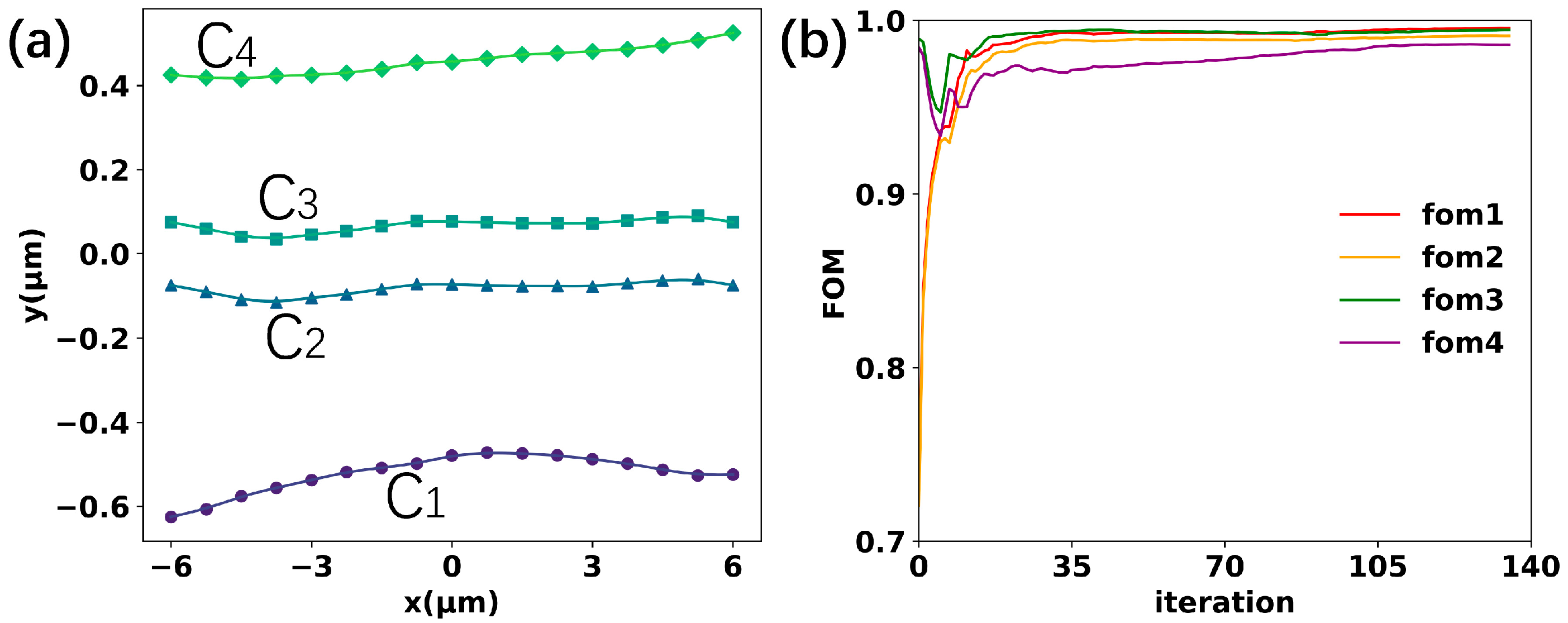
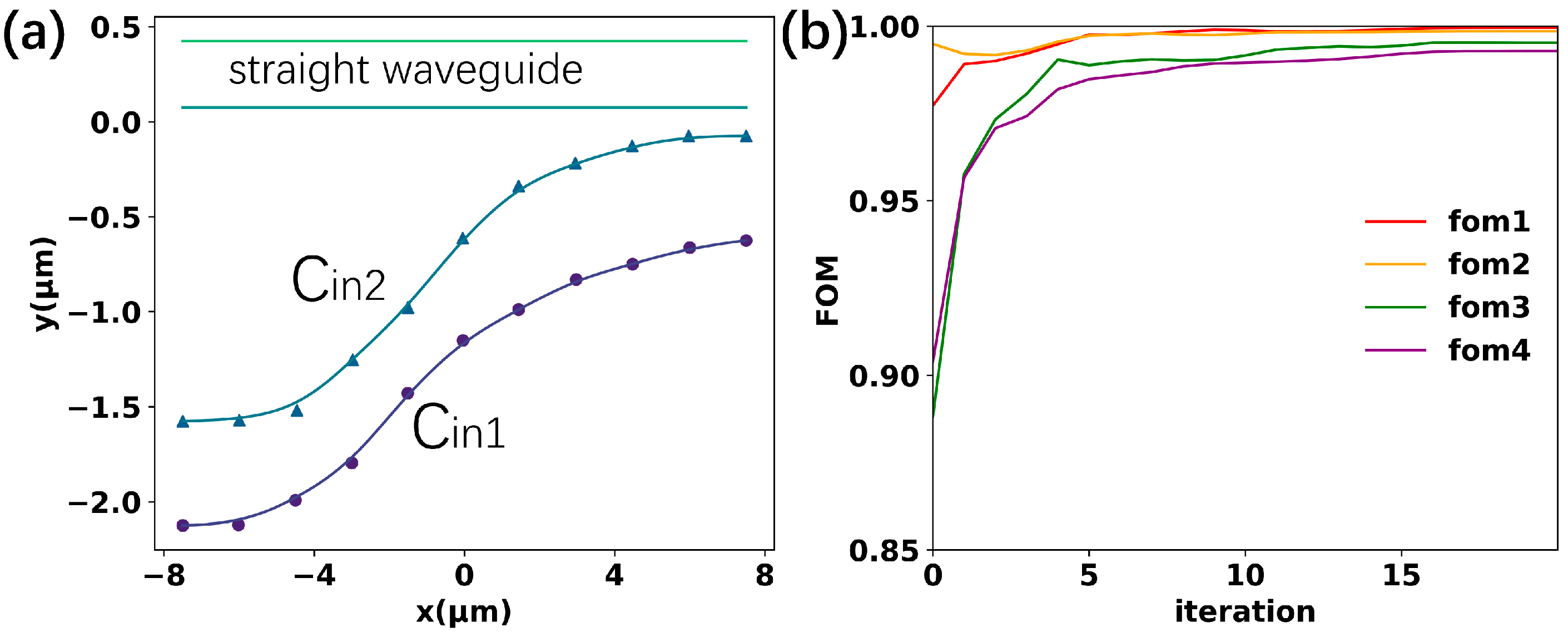
Before starting the optimization, the shape of the four curves in the coupling region was initially chosen to be straight, which also means that the two waveguides were linearly tapered. To realize this shape, the initial coordinates of the control points were uniformly distributed between the first and the last points. The final optimized curve shape is shown in
Figure 3a.
Figure 3b illustrates the evolution of the FOMs with iterations for four modes. After 135 iterations, the FOMs for modes 1 to 4 were 0.9955, 0.9911, 0.9945, and 0.9860, respectively. The iteration procedure took 44 h on a 2.10 Ghz Intel Core 17-12700 PC with 32 GB RAM.
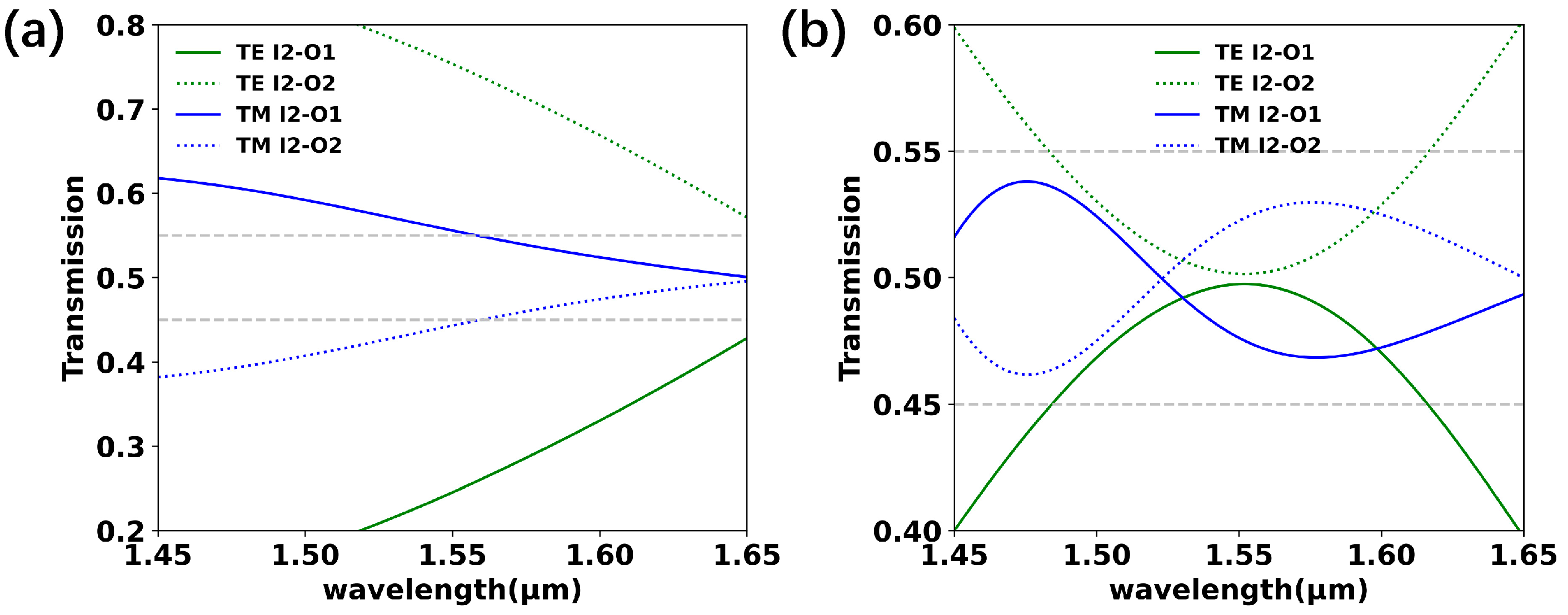
Figure 4a,b show the simulated results of the 2 × 2 3 dB coupler with a standard S-shaped input waveguide of 30 μm length before and after optimizing the shape of the coupling waveguides. As shown in
Figure 4a, the coupling region consisting of two linear tapered waveguides with a length of 12 μm was too short for 3 dB power splitting. After optimizing the shape of the coupling waveguides, the power splitting ratio was maintained within 50% ± 5% for both the TE and TM modes over a wavelength range of 1490 nm–1625 nm, with the IL being lower than 0.06 dB.
When two waveguides get closer, a longer length helps to achieve a lower insertion loss (IL) by reducing bending losses or the excitation of undesired modes. To further minimize the footprint of the device while maintaining low loss, we optimized the S-shaped waveguide in the input region using the same algorithm as the coupling region. The number of control points and the order of the curves were chosen to be 11 and 3, respectively. The optimization was also performed at five equally spaced wavelengths from 1500 nm to 1600 nm. The shapes of the input waveguides of the final optimized curves are shown in
Figure 5a. After 20 iterations, the FOMs for modes 1 to 4 were 0.9996, 0.9985, 0.9952, and 0.9929, respectively. The iteration curves of the FOM are shown in
Figure 5b. The iteration procedure took 29 h on a dual 2.90 Ghz Intel Xeon Platinum 8268 server with 256 GB RAM.
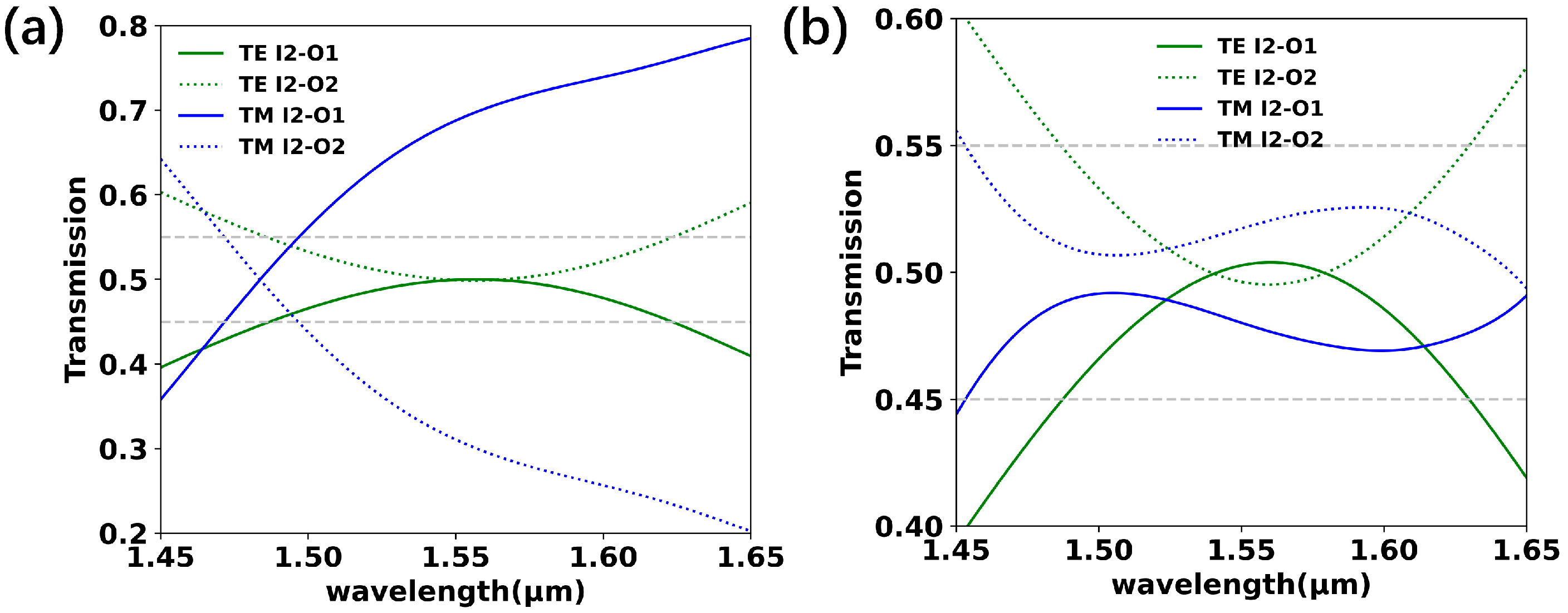
Figure 6a shows the simulated results of the 2 × 2 3 dB coupler with a standard S-shaped input waveguide with a 15 μm length and a shape-optimized coupling region. Shortening the length of the input region significantly reduced the performance of the TM mode.
Figure 6b shows the simulated results of the 2 × 2 3 dB coupler with both the input region and coupling region optimized. After further optimizing the shape of the input waveguides, the power splitting ratio was maintained within 50% ± 5% for both modes over a wavelength range of 1490 nm–1630 nm, with a maximum IL of 0.09 dB.
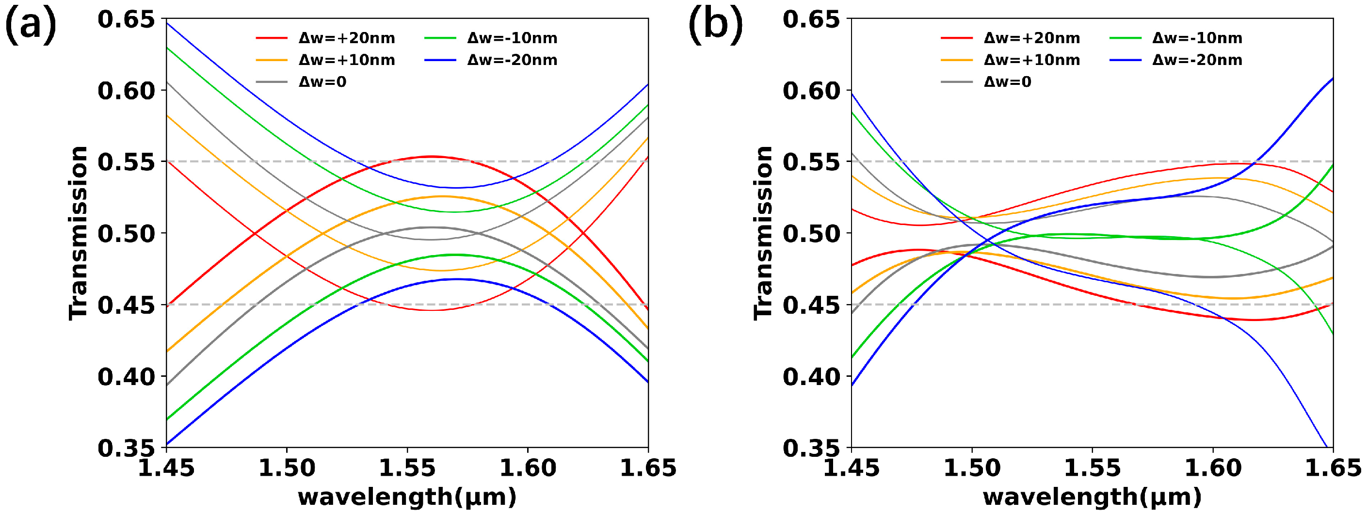
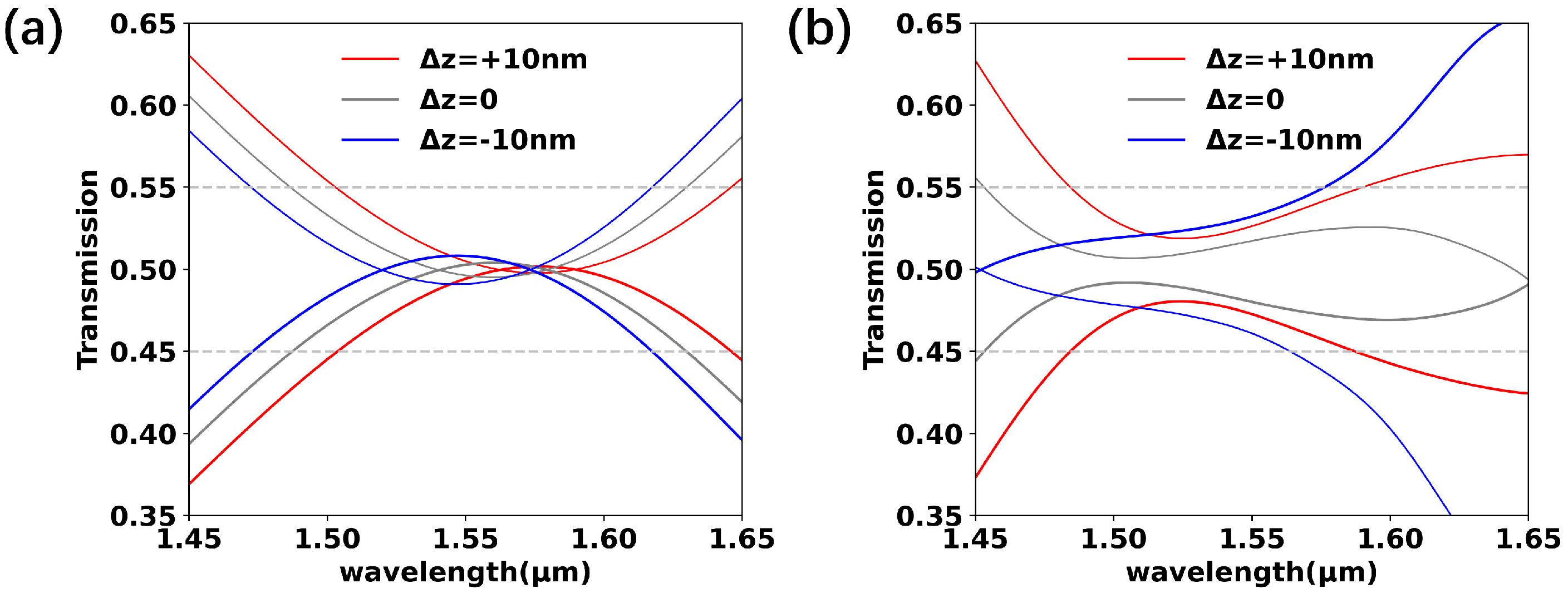
Figure 7a,b show the power splitting ratio of the final optimized device with a waveguide width variation of Δw = 0, ±10, and ±20 nm when light was launched into input I2. The results show that the device can tolerate fabrication errors up to ±10 nm in terms of width variation. The results for a ±10 nm variation in waveguide thickness are displayed in
Figure 8. It can be seen that the spectra of the TM mode were more affected by the thickness of the waveguide.
Figure 9a demonstrates the simulated light propagation profiles of the final optimized device for both polarizations at a 1550 nm wavelength when the light was launched into input I1 and I2, respectively. It can be seen that the operation of the TE mode was based on adiabatic evolution. In the case of the TM mode, the 3 dB power splitting was actually realized based on mode coupling in a quasi-adiabatic regime.
3. Fabrication and Experimental Results
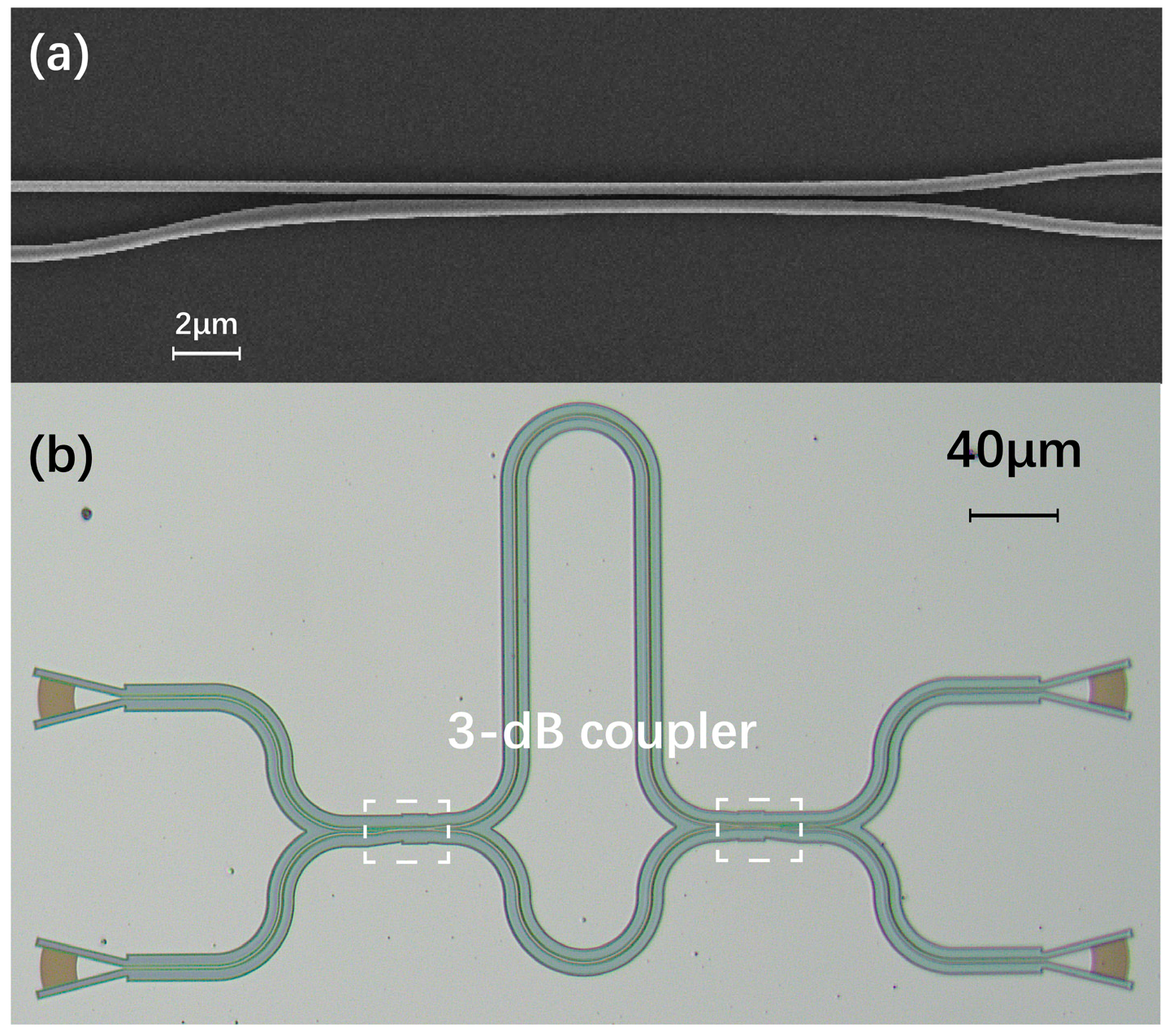
The device was fabricated through the SOI platform with a top silicon thickness of 220 nm and a buried oxide layer thickness of 3 µm. The fabrication process began with electron beam lithography (EBL) to define the pattern, followed by inductively coupled plasma (ICP) etching to transfer the pattern onto the silicon layer. Finally, a 3 µm thick upper silica cladding layer was deposited by plasma-enhanced chemical vapor deposition (PECVD).
Figure 10a shows a scanning electron microscope (SEM) image of a fabricated 2 × 2 3 dB coupler.
Figure 10b shows a microscope image of an unbalanced Mach–Zehnder interferometer (MZI), which was used to characterize the power splitting ratios of the device, and the difference in the length between the two arms was ΔL = 150 µm for the TE mode and ΔL = 250 µm for the TM mode.
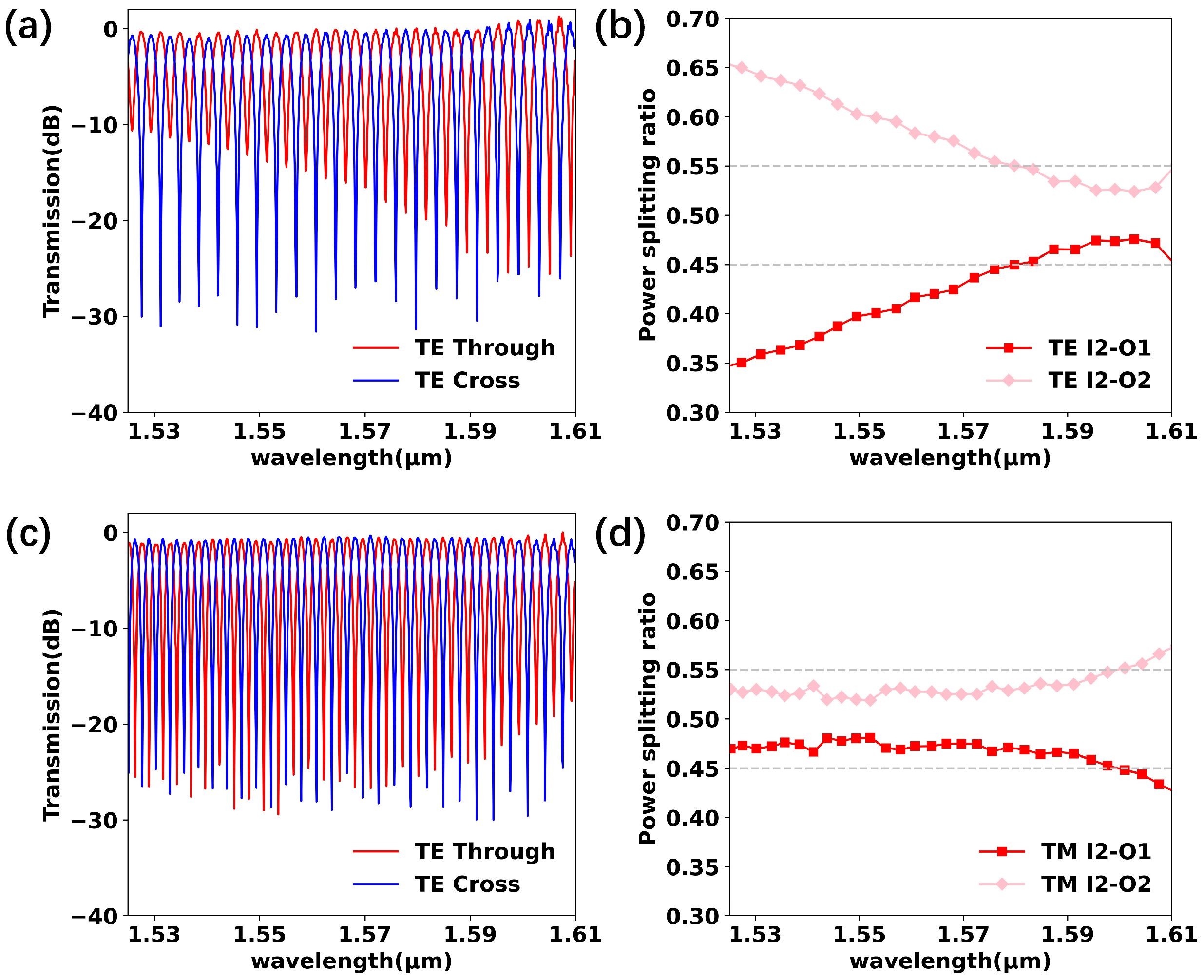
To characterize the performance of the fabricated devices, an amplified spontaneous emission (ASE) broadband light source with an operating wavelength range of 1525 nm–1610 nm and an optical spectrum analyzer (OSA) was employed. The measured spectra of the unbalanced MZI and the power splitting ratios K of the 3 dB coupler are displayed in
Figure 11. Here, K was calculated from the extinction ratios (ERs) of the measured spectra according to the following equation [
9]:
As displayed in
Figure 11, the TM mode achieved a power splitting ratio within 50% ± 5%, ranging from 1525 nm to 1600 nm. Meanwhile, the TE mode only achieved the desired power splitting ratio in the range of 1576 nm–1610 nm. The measured ILs of a single device for both polarizations were less than 1 dB. The results suggest that the boundary of the fabricated 2 × 2 3 dB couplers deviated from the design. Comparison with the fabrication tolerance analysis in
Figure 7 and
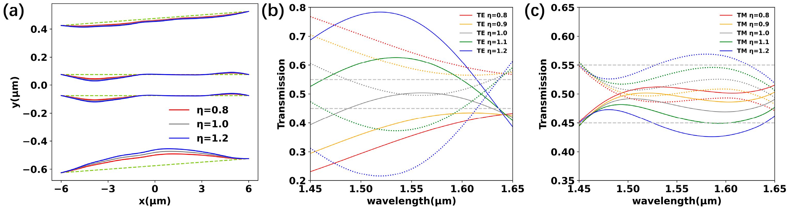
Figure 8 does not provide a good explanation for the apparent deviation in the experimental results of the TE mode from the simulation results. We believe that the deviation came from a particular kind of fabrication imperfection in the coupling region. We modeled the deviated curves
by adding a variable controlled by the parameter η on the curves
. Specifically, the curve equation can be defined as follows:
where η was used to control the generation of manufacturing error, and η ranged from 0.8 to 1.2. When η was less than 1, the curve approached towards the line segment whose endpoints coincided with the curve’s endpoints, appearing as under-etching with a non-uniform magnitude at different locations. Conversely, when η was greater than 1, the curve moved away from the line segment, appearing as over-etching with a non-uniform magnitude at different locations.
Figure 12 illustrates the deviated curves and transmission spectra for different η values. As is apparent in
Figure 12b,c, the power splitting ratio in the TE mode was more sensitive to η than that in the TM mode. In addition, the experimental results of the TE mode were consistent with η < 1, indicating that the error came from the curve shape deviation caused by localized under-etching.
From a design perspective, we considered the following methods to mitigate the effects of such deviations: (1) appropriately increase the length of the coupling region; (2) not optimize the shape of the gap (curves C2 and C3) to reduce the effect of the simultaneous deviation of curves on both sides of the waveguide; (3) change the number of control points and the order to further improve the smoothness of the curves; (4) add some random errors during the iteration process to improve the robustness of the optimization results.
Table 1 summarizes the performance of our device and state-of-the-art polarization-insensitive 3 dB couplers built on the SOI platform with a 220 nm core silicon thickness. From the simulation results, our optimized design resulted in a more compact 2 × 2 3 dB coupler with broader bandwidth and lower loss. However, the fabrication tolerance of our design was not as high as expected, making the experimental results of the TE mode deviate excessively from the design.


