Abstract
This work reports the design of a 1x2 photonic digital switch controlled by an electrically induced metasurface, configurated by a rectangular array of points where the refractive index is locally changed through the application of an external bias. The device is simulated using the Beam Propagation Method (BPM) and Finite Difference Time Domain (FDTD) algorithms and the structure under evaluation is an amorphous silicon 1x2 multimode interference (MMI), joined to an arrayed Metal Oxide Semiconductor (MOS) structure Al/SiNx/a-Si:H/ITO to be used in active-matrix pixel fashion to control the output of the switch. MMI couplers, based on self-imaging multimode waveguides, are very compact integrated optical components that can perform many different splitting and recombining functions. The input–output model has been defined using a machine learning approach; a high number of images have been generated through simulations, based on the beam propagation algorithm, obtaining a large dataset for an MMI structure under different activation maps of the MOS pixels. This dataset has been used for training and testing of a machine learning algorithm for the classification of the MMI configuration in terms of binary digital output for a 1x2 switch. Also, a statistical analysis has been produced, targeting the definition of the most incident-activated pixel for each switch operation. An optimal configuration is proposed and applied to demonstrate the operation of a digital cascaded switch. This proof of concept paves the way to a more complex device class, supporting the recent advances in programmable photonic integrated circuits.
1. Introduction
Integrated photonics represents an unmatched opportunity for implementing a large variety of programmable functions [1,2], and a large-scale implementation of fabrication facilities for Photonics Integrated Circuits (PICs) may be expected in the near future, targeting an economy of scale comparable to the one attained by in microelectronics. There is great expectation for this roadmap [3] aiming for application-specific integrated circuit (ASICs) standardization of the overall process, from design simulation to the fabrication-packaging steps [4]. There has been great interest in the application of photonic switching structures [5], aiming for the development of programmable devices for optical data processing [6]. An interesting approach recently reported used nanostructured material geometry to create an arbitrary distribution of the refractive index values, permitting power splitting with arbitrary input and output directions [7]. The combination of a Deep Artificial Neural Network with the optimized design of a local perturbation for the refractive index in nanophotonic structures has opened a path toward the fabrication of universal optical components [8]. Considering that while the overmentioned examples are based on a lithographic design to produce a device associated with a specific function, there is also a large investment in the scientific community in developing proper layouts for programmable integrated circuits, compatible with standard CMOS fabrication technology and capable of addressing a wide range of applications by providing a higher-level platform for prototyping novel optical functionalities without the need for custom chip fabrication [9]. PICs manipulation of light flow is based on a tunable control operated on switching devices, over an array of switches connected by waveguides. Programming functionality allows the implementation of a wide set of logical functions, leading to the conception of a general-purpose photonic processor to leverage the unique properties of photonics in terms of ultra-high bandwidth, high-speed operation, and low power consumption [10]. The switching operation in the devices proposed and described in the literature is typically based on phase shifting control, operated on a set of light couplers conveniently distributed and mutually interconnected. The phase-shifting function is generally operated by the thermo-optical effect [11]. For reducing the power requirements of these systems, novel approaches using liquid crystals [12] and/or MEMS [13] structures have been proposed as an alternative to heaters, in line with the general recommendations for the next generation of energy-efficient smart edge devices.
More recently, externally induced material phase changes have also been demonstrated, allowing reconfigurable bistable functions [14], giving rise, among other applications, to the proposal of efficient structure for non-volatile memory storage with reconfigurable memory addressing to be used in photonic computing architectures [15].
While MxN digital optical switches have been studied since the gold times [16,17], a large effort is presently being applied to produce advancements in photonic-electronic integrated circuits for computing and AI tasks. Targeting the full implementation of the photonic tensor core, one main research direction is the search for novel device concepts and photonic material integration [18]. A programmable photonic structure based on the MMI features, named Function Programmable Waveguide Engine (FPWE), has been recently presented and demonstrated to be applicable in developing cascaded switches and logical gates, built upon a combination of electrical inputs and optical outputs [19]. The 1xN switch functionality has gained increasing consideration for possible applications in optical communication networks, supporting large port count optical devices for big data and artificial intelligence, and boosting the use of materials requiring a simplified fabrication process [20]. Due to the complexity of the layout of these kinds of structures, a deep learning approach has been chosen as an effective tool to optimize the device geometry and its correlation with the desired functionalities [21]. Whenever functional meta-components need to be configured, improving the optical performances is supported by machine learning algorithms for optimization and inverse design [22].
Independently of the underlying physical effect, the switching mechanism depends on the fine-tuning of the refractive index of suitable materials incorporated in the device. Thus, the integration of subwavelength-structured metasurfaces and metamaterials on the standard optical waveguides can be suited to the proper design of a variety of meta-waveguides with unprecedented control capabilities [23]. Within this context, the application of machine learning techniques grants the project of metamaterial-based devices [24] that can be fabricated in the traditional semiconductor process. The neural network method for the optimization of metamaterial-based devices permits us to overcome the intrinsic limitations of conventional design, allowing an inverse design approach for metamaterial-based devices [25]. From this point of view, a deep learning model can be used to determine the output spectrum of a specific photonic device, using the nanostructured geometry of the material as an input. The supervised model needs to be trained with a large dataset of input/output points obtained from simulation, but once trained, it can be used to accurately approximate the output spectrum of a metamaterial much faster than using direct simulations [26]. The inverse problem can also be solved using a deep learning model by using the outputs as inputs and training the network to find the configuration for a particular output.
One of the most important limits for a large-scale commercialization of Photonic Integrated Circuits is the manufacturing tolerances that strongly degrade the PICs fabrication [27]. While nanoimprint lithography is generally accepted as a technology with great potential to approach these problems [28,29,30] an alternative approach, based on a waveguide with a multi-micron dimension, allowing a better polarization and process tolerance management, has been recently proposed [31]. In agreement with these considerations, the increased fabrication tolerance induced by a multi-micron dimension paves the way for a new efficient use of hydrogenated amorphous silicon (a-Si:H) deposited by the Pressure Enhanced Chemical Vapor Deposition (PECVD) method [32]. State-of-the-art good quality a-Si:H can be deposited by PECVD as this technique has reached a stable maturity and quality, due to the large investment directed to mass production of a-Si:H solar cells [33] and thin film transistor for active-matrix flat panel displays [34]. The electro-optical effects in silicon were well described and theoretically supported by Soref in 1987 [35], where the charge carrier effect is reported to produce a modification of the semiconductor refractive index up to an order of 1–10%.
Based on the same, adapted, Soref model, electrooptic modulators based on a-Si:H material have been dimensioned and fabricated [36,37]. Indium thin Oxide (ITO) has been observed to exhibit a huge enhancement of the non-linear optical response [38] and proposed as a good candidate for nonlinear photonics metasurfaces [39]. Such peculiar characteristics have been exploited for ITO-Silicon integrated structures in very attractive structures for photonics neural network applications [40] and reconfigurable devices where the ITO/Si structure acts as a localized MOS capacitor island [41].
Taking into consideration all the application opportunities and the technology requirements presented above, following a methodology previously introduced by the authors [42], this work presents a feasibility study about an alternative switching structure. The study is based on numerical simulations performed using the RSOFT Photonics Packages FDTD and BPM algorithms via a University Donation Program [43]. The proposed solution joins the multi-micron approach to the switching functionality and the specific electro-optic properties of amorphous silicon. The typical light splitter/coupler multimode interference structure (MMI) configuration is interfaced with a reconfigurable pixeled metasurface, producing a building block suitable to be used as a photonic digital 1x2 switch. The configuration proposed, where each MOS “pixel” produces a local alteration of the refractive index, is only possible with the use of amorphous silicon. In fact, due to its intrinsic low conductivity, a-Si:H lateral transport effects are naturally confined to the region of the charge source [44,45], as has been extensively reported in previous works targeting imaging devices [46]. Therefore, limiting the crosstalk between neighbor MOS pixels, amorphous silicon appears to be a natural choice for the idea hereby proposed, based on joining the concept of metamaterial-based devices with PECVD materials and Active-Matrix control.
2. The Optical Phase Shifter
The main building block for a programmable PIC is a 2x2 switch, and the standard approach for implementing a programmable functionality is based on the thermo-optic effect, by employing an electrically controlled heater on the waveguide surface and inducing a slight change on the semiconductor refractive index.
The working principle of the thermo-optics effect is to alter the refractive index of the waveguide and cladding material by means of injecting a current into a resistive heater along them. At a specific wavelength , the resulting variation of the refractive index () induced by a change in the temperature () is controlled through the effective thermo-optic coefficient of the semiconductor ().
where, according to joule heating, the temperature increase is directly proportional to the power consumed by the microheater, denoted as .
The refractive index modulation speed can be evaluated by a time constant , denoting the switching time, measured in microseconds (), determined as: [47]
where is the thermal conductance between the heated waveguide and the heater, is the heat capacity of the heated arm including the area traversed by the heat flux (Gap). The typical configuration for a refractive index controller based on the thermo-optic effect, is reported inn Figure 1.
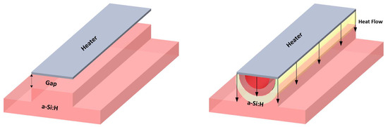
Figure 1.
A typical configuration for a refractive index controller based on the thermo-optic effect.
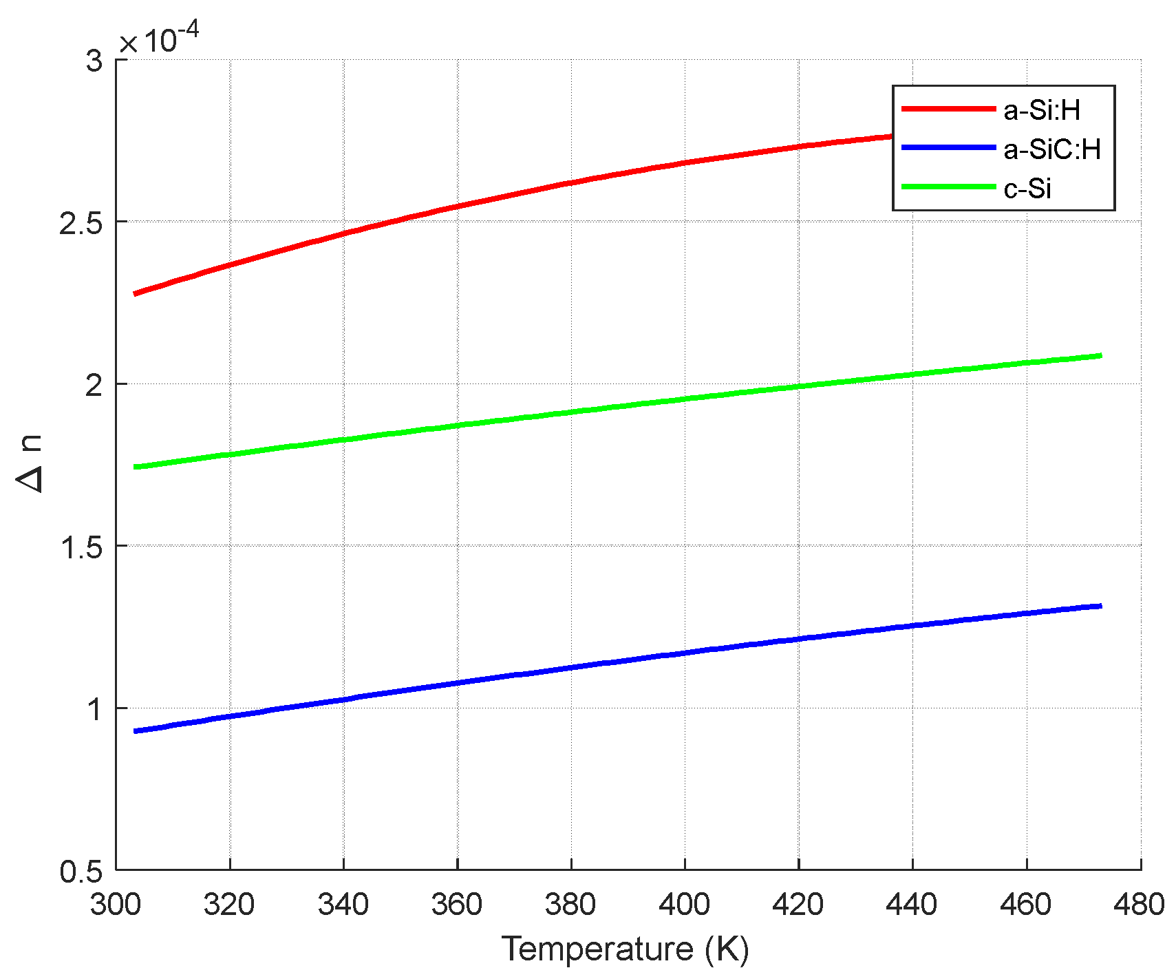
The thermo-optic coefficients of a-Si:H have been measured in operation temperature range 300–500 K, at the communication wavelength of 1550 nm [48]. The experimental data have been fitted using a single-oscillator model:
which results in a variation stronger than the one observed in crystalline silicon. The thermo-optic coefficient of a-Si:H at room temperature is estimated to be 2.3 × 10⁻⁴ K−1 [49], about 20% higher than that of c-Si [50].
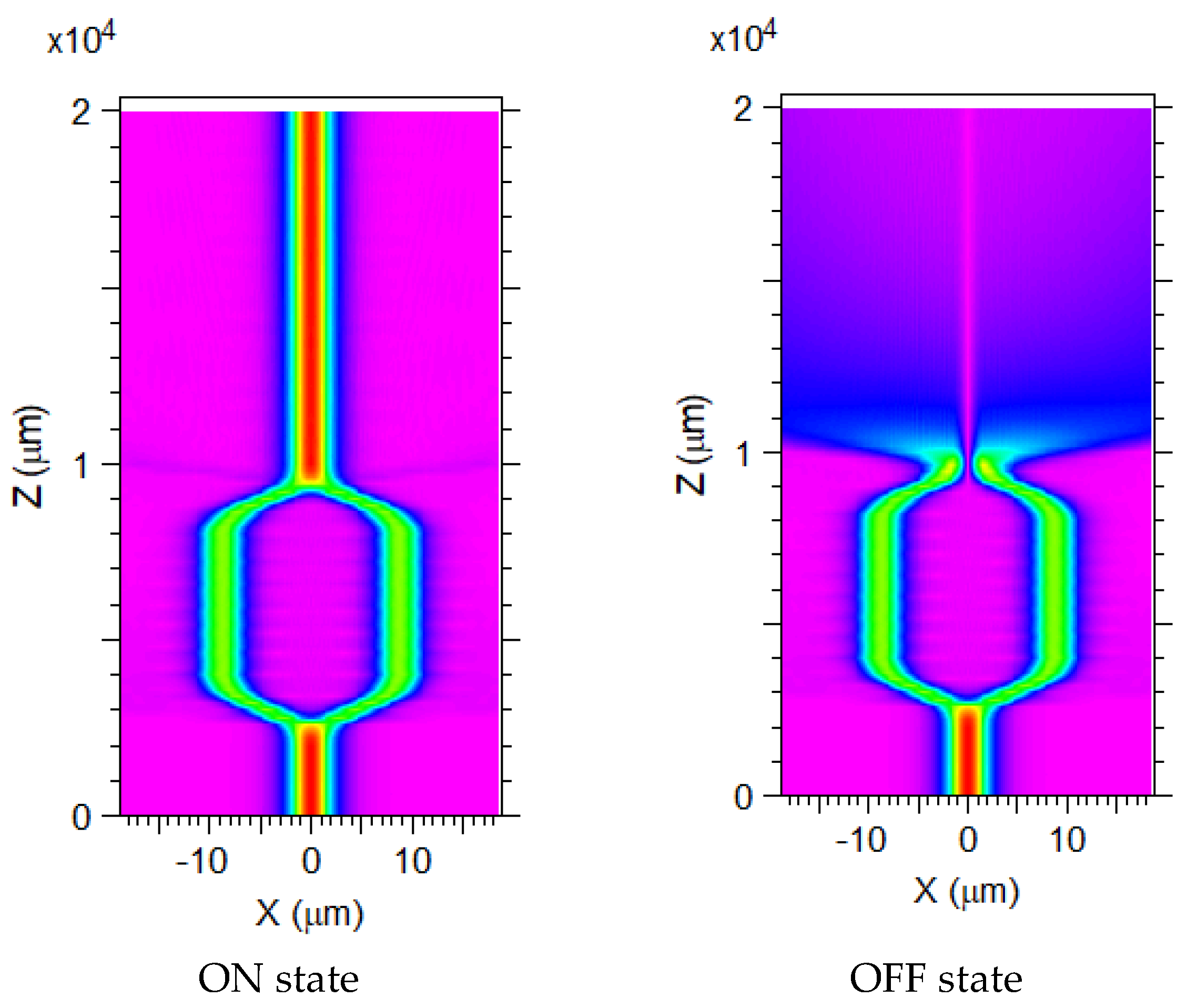
Figure 2 and Figure 3 report the simulated results about the index change over a temperature variation of 100 K. The extent of the index variation is present but limited to small values, which leads to a standard geometry for an interferometric switch with dimensions in the order of magnitude of tenths of millimeters (see Figure 4). While the PECVD deposition technique is prone to handle the fabrication of large area devices, the uniformity of the lithographic process can be a challenge requirement to be fulfilled. A largely exploited alternative is based on the electro-optic effect induced by free carrier accumulation, extensively described in silicon [51] as having a refractive index change up to 10−2 for the wavelength of 1550 nm and even higher in a-Si:H the because of the presence of the trapped carriers at localized states [52]. Yet, the dimension of the phase shifter, necessary for an On-Off function, remains higher, limiting the fabrication of Programmable Pics with a large number of switches. So, other alternatives approaches have been proposed to address the problem of scaling PICs dimension, like phase change materials, liquid crystal based, MEMS, Piezo or Pockels [53]. In the following of this manuscript, we propose the Meta-MMI as alternative switching structure with reduced dimension.
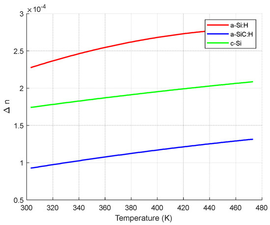
Figure 2.
Graphical representation of the thermo-optical coefficient models described in [45,46].
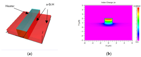
Figure 3.
Temperature-induced variation of the refractive index of an a-Si:H waveguide. Simulated structure (a) and the spatial distribution of the index change (b).

Figure 4.
On-Off function of an a-Si:H interferometer controlled by thermo-optic effect.
3. The metaMMI Model
An analytical description of self-imaging in uniform index slab waveguide multi-mode optical waveguides of homogeneous refractive index was first presented by Ulrich in 1975 and successively elegantly described by Soldano [54] as a property of multimode waveguides by which an input field profile is reproduced in single or multiple images at periodic intervals along the propagation direction of the waveguide. According to this theory, multiple images of the input filed can be found at periodic distance Lp which, in turn, depends on the width of the planar waveguide, the light wavelength, and the effective index of the input mode. The MMI structure takes advantage of these properties allowing flexible splitting functionalities. When compared with other structures, like, for example, the directional couplers, the MMI presents higher tolerance to dimension changes in the fabrication process by not requiring submicron lithography gaps, has a large optical bandwidth, and has a low polarization dependence. Following this path, it becomes possible to design MMI layouts with an arbitrary number of multiple input and output ports. Violating the symmetry of the components, for example, the position of the input channel, as reported in Figure 5 the constructed self-images reflect the asymmetry, and it is possible to route the output on a specific channel. Anyway, in this case, some of the attractive characteristics of the MMI splitters, like the invariance of the losses to an increasing number of input/output are reduced. The asymmetry proposed in this work is produced by a reconfigurable array of local controllers for the refractive index. To address this point, a study was performed on the number of output channels and the dimension of the main MMI body. Regarding the first point, we have found that

Figure 5.
MMI output asymmetry induced by the position of the input waveguide in a 1x3 splitter.
MMI couplers, based on self-imaging multimode waveguides, are highly compact integrated optical components that can perform multiple different splitting and recombining functions. The underlying self-imaging principle, in multimode waveguides, is described using a guided mode propagation analysis and an optimal configuration can be analytically calculated [55]. Anyway, when the device geometry becomes irregular, an analytical approach is no longer possible, and the solution can be obtained only by the application of numerical simulation techniques [56].
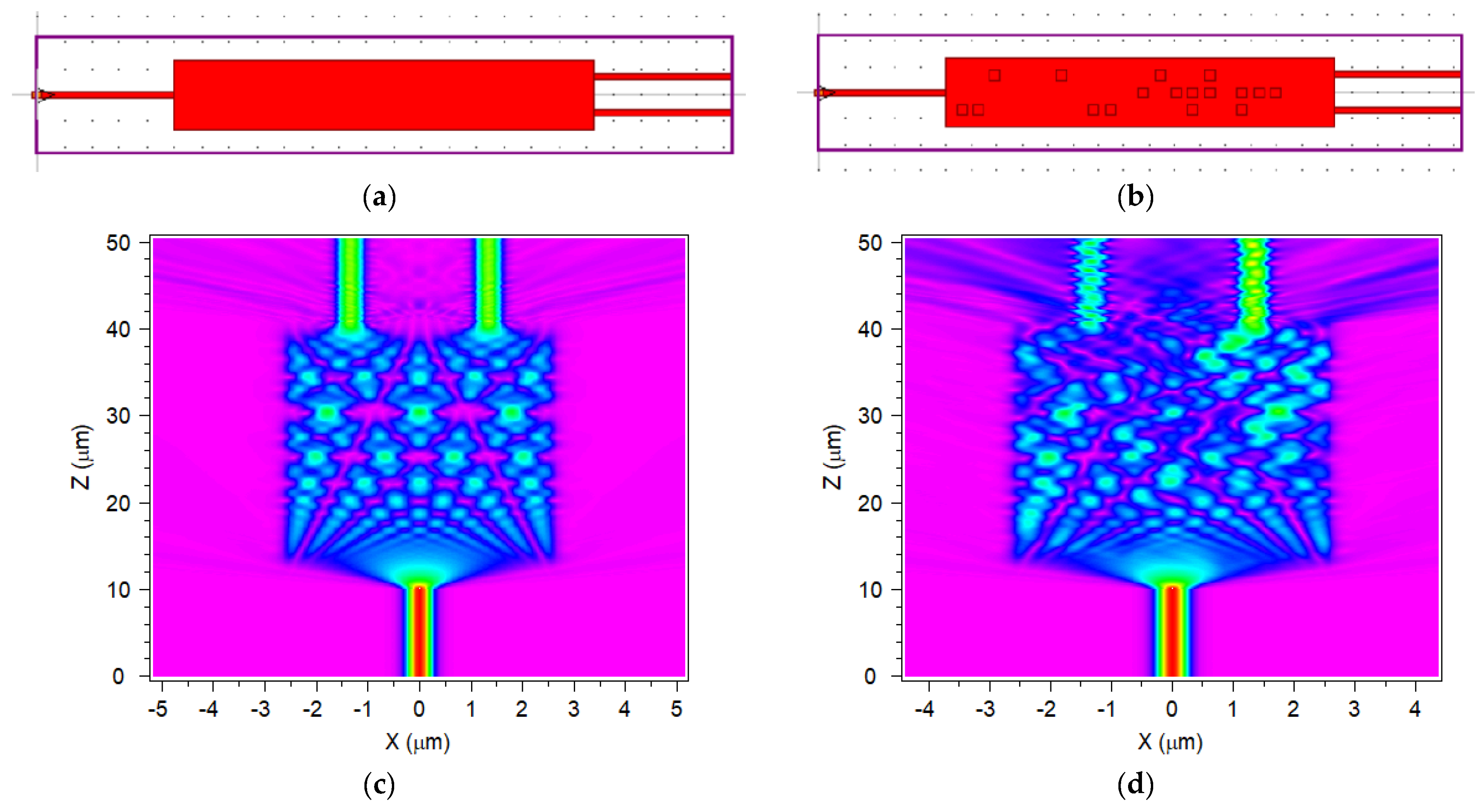
As a first step, we have simulated and optimized the MMI behavior. It can be observed in Figure 6c that if all the MMI dimensions are optimized, the field entering through the input port is equally divided into two output channels. This configuration (Figure 6a), typical in splitter devices, is very sensitive to the parameter defining the device geometry, the material used, and the light wavelength.
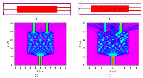
Figure 6.
Simulation layout of basic MMI structure (a), the MMI interfaced to a metasurface (b) and the correspondent calculated EM field inside the MMIs. In the basic structure (c) the input light is equally split in the two output waveguides, while in the MMI controlled by the metasurface, the output balance is changed (d).
The second step is the introduction, in the simulation layout, of an array of small square regions where the material optical properties (i.e., the refractive index) are locally modified Figure 6b. Consequently, light propagation inside the MMI is also modified, and the light intensity at the output channels changes conveniently (Figure 6d). This configuration can be considered as an externally induced metasurface in the MMI main body.
Such metasurface effect could be created and controlled by a MOS structure deposited on top of the semiconductor surface, where the charge accumulation induced at the surface by an externally applied voltage, together with the thin dimension in the vertical dimension of the photonic layer produces a small change in the semiconductor refractive index that can be approximated by a uniform vertical distribution. Figure 7 reports a sketch of the proposed MOS-controlled metasurface, as we have introduced it in our simulations.
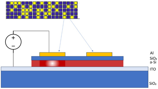
Figure 7.
MOS controlled metasurface. The white region represents the charge accumulation when an external bias is applied to the metal contacts.
Indeed, the perturbation induced on the refractive index depends on the concentration of the accumulated charge, which in turn depends on the MOS structure and on the applied voltage. Finally, once one knows the induced charge accumulation, the new refractive index can be calculated by the Soref model. This model relies on the Drude theory and it describes the variation of the refractive index (Dn) with the charge accumulation (Ne and Nh) be summarized by the following expression:
where ε0 is the vacuum permittivity e is the elementary charge, n the unperturbed refractive index of the material, m* denotes the carrier effective mass, and the subscripts e and h label quantities associated with electrons and holes, respectively.
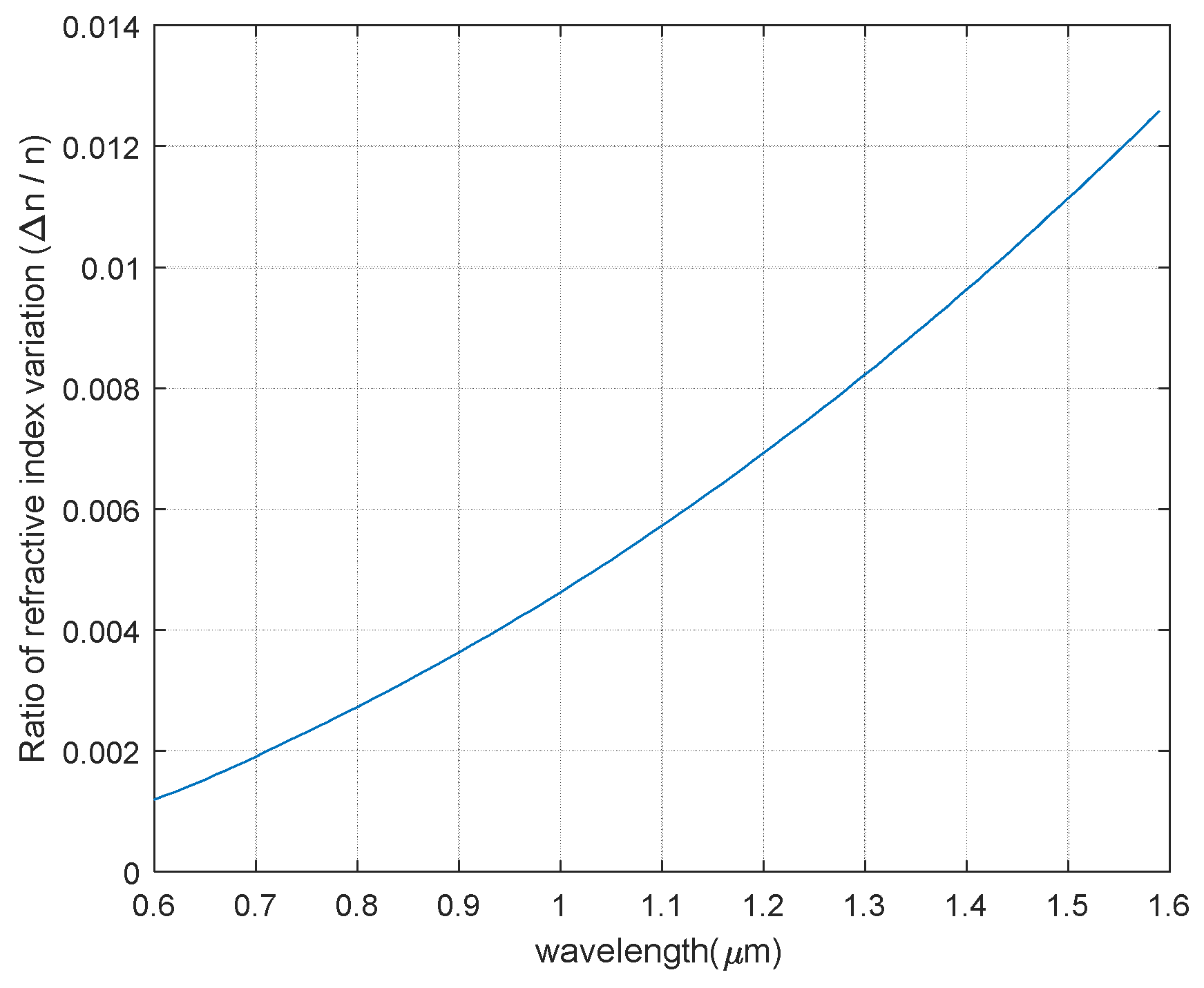
Figure 8 depicts the variation of the refractive index, calculated by the Soref model, induced in amorphous silicon by a charge accumulation of 1019 cm−3 for a wavelength interval in the visible and near IR range. It may be observed that in the near-infrared region, the induced variation is about 1%. This model does not take into account the saturation of free-carrier-induced index change, so, for a detailed calculation, it should be given special attention to this point. Furthermore, the presence of trapped charge in defect states of amorphous silicon is expected to boost the charge accumulation process and consequently the electro-optic effect.
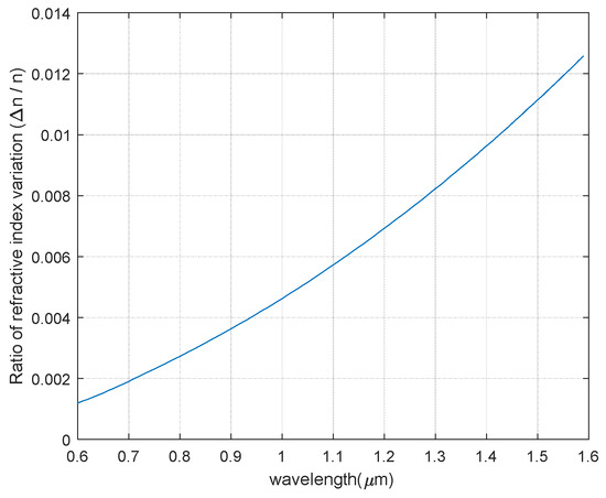
Figure 8.
Ratio of the refractive index variation over the corresponding value as a function of the wavelength. The values are calculated by the Soref model.
The fine-tuning of the electrically controlled refractive index was not studied in detail in this work, and our conclusion about its feasibility relies on the well-established technology for Thin Film Transistors (TFTs) supporting Active Matrix Displays [57].
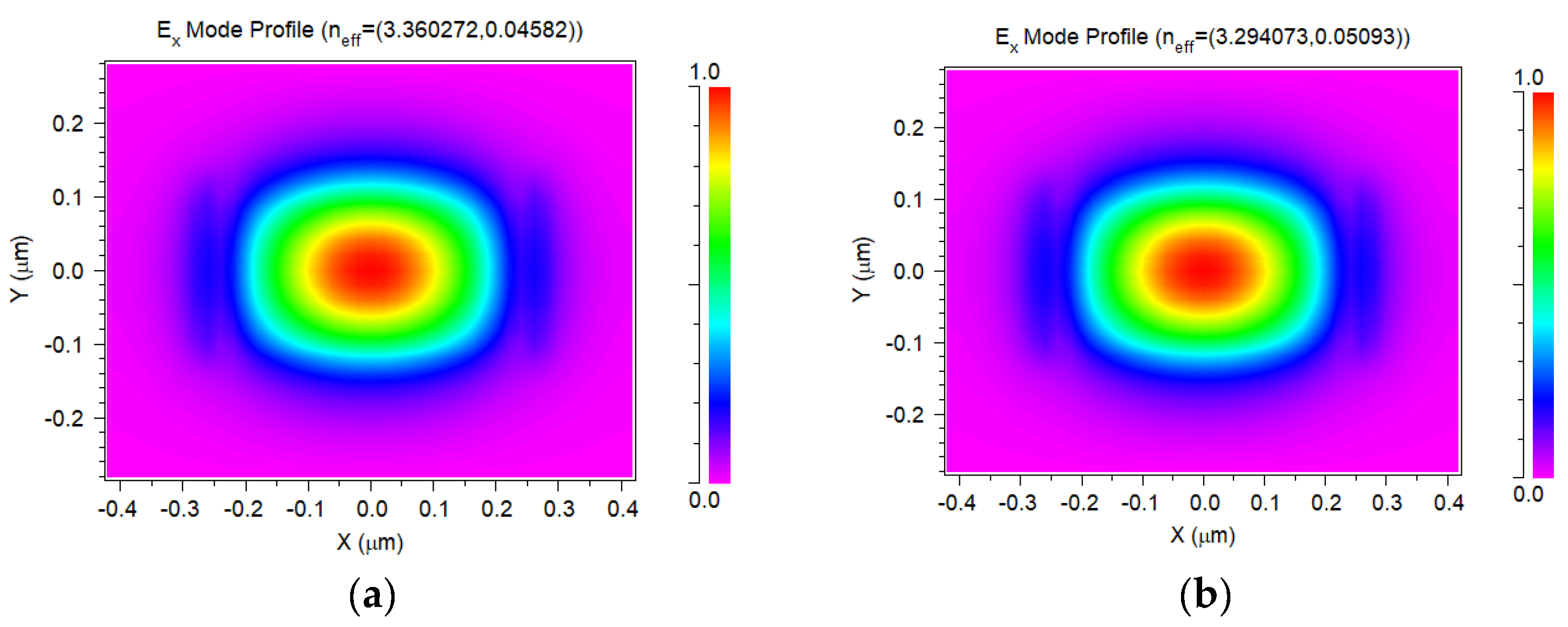
The thermo-optics-based phase shifters offer efficient and stable modulation, but the free-carrier-dispersion-based modulation is preferred in applications requiring high-speed phase modulation, such as telecommunications [58]. Charge accumulation is usually performed using a p-n junction or a metal-insulator-semiconductor (MIS) structure. The capacitance per unit area in a MIS structure is the main parameter influencing the responsivity, but when the dimension is reduced to the nanoscale, it may be observed a significant enhancement of the inversion effect and a decrease in the response time. Consequently, nanoscale MOS capacitors are revealed to be a promising device for active electro-optical modulation [59]. The metaMMI structure hereby proposed attempts to profit this MOS characteristic, by keeping the area of the single pixels as small as possible, aiming to generate a small total capacitance for the control matrix and consequently targeting a fast time response. At the present stage, our approach targets mainly the demonstration of the metasurface effects, to control the output of a reconfigurable switch, so the physical considerations about the material properties, even if of major importance in a fabrication step, will be further addressed in a second time, together with the specific requirements from the selected facilities for the device fabrication. The semiconductor used in our simulation is amorphous silicon, with a refractive index naSi = 3.42149, deposited on an ITO substrate [60]. Covered by a SiO2 layer with nSiO2= 1.4551. By a straightforward calculation, as reported in literature [61], over a MOS structure ITO/SiO2/a-Si:H the bias application is expected to produce a charge accumulation in the range 1019–1020 cm−3, being possible to control this value through the modulation of the oxide layer thickness. Such charge accumulation corresponds to an index variation spanning in the range 0.01–0.22 [52]. As an example, Figure 9 reports the TE00 mode within an a-Si:H waveguide with no charge accumulation compared with the case of a charge accumulation of 1020 cm−3; it is possible to observe that the effective modal index reduction is of the order of 10−2.
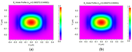
Figure 9.
TE00 mode within an a-Si:H waveguide with no charge accumulation (a) and with a charge accumulation of 1020 cm−3 (b).
In our simulation, we have assumed the MOS activation to induce a variation in the refractive index of 0.01%. This value is in the range of what is reported in the literature for crystalline silicon [62] and below the values that could be expected in the amorphous counterpart by exploiting the localized charge trapping due to the unavoidable presence of midgap density of states. Additionally, the choice of amorphous silicon allows taking profit from the high resistivity of the material, reducing lateral charge diffusion [63] and its related cross-talking effects. In Figure 4 it was possible to see the device simulation layout, and the results obtained by the simulation, as well as the impact of a random distribution of activated MOS on the output channels.
Once the objective of the study is defined, it is necessary to design a 1x2 MMI layout suitable to host on its surface a matrix array of contacts with dimension and density capable of imposing control on the light intensity of the output channels. The same standard 1x2 3 dB splitter function can be obtained by varying conveniently the length (LMMI) and the width (WMMI) of the MMI box. Following a preliminary study, our choice has been guided by the following requirements, where the dimension of the structure is maintained within the limits of a standard lithography process:
- The size of each metal contact should be larger than 0.5 mm2.
- The separation between adjacent metal contacts should be at least 0.5 mm.
- The number of metal contacts should be maintained as small as possible
- The MMI should perform an optimized 3dB splitting function when no bias is applied to the metal contacts.
- By varying the activated MOS contacts, each of the output channels should allow an independent and continued variation of the light intensity.
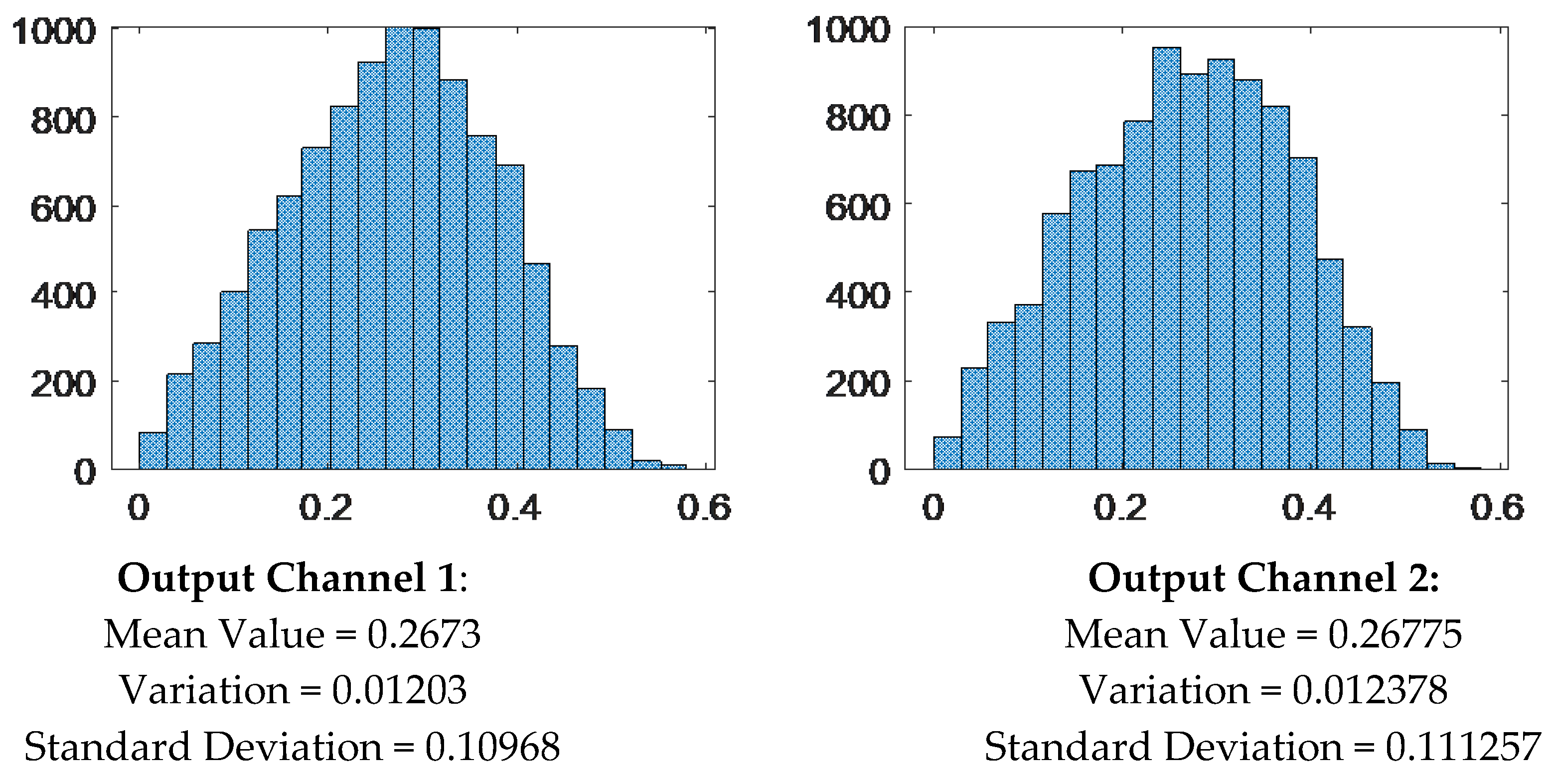
Considering these requirements, we have chosen an MMI with dimensions LMMI = 30.55 mm and LMMI = 5.2 mm. This small footprint allows complete control of the output channels with a 3x20 MOS array where each metal contact is a square with a 0.8 mm side. On the active control of the MOS array, we have imposed a rule for maintaining an average of 70% of the contacts in the ON state, while the other 30% is kept in the OFF state. This choice allows for the possibility of having one of the output channels with full light intensity while the other one receives no light. This configuration, interesting from the digital application point of view, cannot be completely attained with a lower number of contacts in the ON state. Figure 10 reports a simple statistical analysis of power distribution on each of the two channels, obtained on a set with 1000 samples, randomly generated, yet respecting the optimal condition described above. The channels are symmetric and each one spans between 0 and 50% of the input power. The layout of the metasurface has been tailored to be able to produce output configurations for all the classes in analysis. So, the number of array elements, their size, and position have been chosen in order to allocate 10% of the total number of simulated results in the most asymmetric classes (1, 0) and (0, 1).
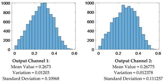
Figure 10.
Histogram of the distribution of the power level at the output channels, calculated on a set of 1000 samples randomly generated. On the x-axis the fraction of the power is reported, calculated on the input power, while on the y-axis the number of occurrences is reported.
4. Database Creation and Analysis
As previously put in evidence, the input–output relationship cannot be defined either as a full input–output map, or as an analytic function; the first one due to the fact that the input size is , the second for the complexity of the structure and the phenomena involved. The choices adopted here consist of the use of a subset of possible input combinations, with the corresponding output obtained by simulations previously described, and the identification of common characteristics when the same output is produced. The first attempt makes use of a machine-learning-based approach for the model definition: the common characteristics detection is demanded to a suitable neural network training, whose effectiveness is measured by a confusion matrix, discussed in the next Section. To this aim, using the the model and the layout described in Section 2, it has been produced a database with 105 simulations, obtained using the BeamProp method.
The BPM method exploits finite difference methods to solve the parabolic, or paraxial, approximation of the Helmholtz equation [64], implementing transparent boundary conditions. Despite some mitigation techniques implemented in the RSOFT package, the main physical limitation of the parabolic approximation of the Helmholtz equation is the difficulty of simulating sharply curved waveguides [65]. A second limitation of the described approach arises from the assumption of scalar waves, which do not allow the effects of polarization to be considered. One additional limitation of the BPM algorithm is that it cannot account for backward reflections, limiting the analysis to the one-way wave equation. While the first two limitations have no impact on our work, the back reflection can be an issue in MMI functionalities. Anyway, RSOFT BeamPROP has a bidirectional BPM algorithm [66], which considers coupled forward and backward traveling waves, and can account for reflection phenomenon, including resonant effects. Despite these limitations, we have adopted the BPM method for database creation due to its attractive execution time and computer memory management. All the results have been confirmed by FullWAVE FDTD simulation at the end of the analysis, dispelling doubts regarding the back-reflection effects.
Each simulation run has a different configuration of the ON-OFF distribution state of the electric contacts. The result of each simulation run has been classified on the basis of the power reading on the output channels. For the output definition, two different approaches have been attempted, where the power intensity has been discretized on 3 or 5 levels, yielding to the output sizes or respectively. In the 3-level configuration, the thresholds, defined on the power fraction, separating the different classes are 0.05 and 0.35 for the lower and the higher level, respectively. So, we have level 0 representing the dark state (power between 0 and 0.05), level 1 represents the light state (power higher than 0.35), and an intermediate level 2 (power between 0.05 and 0.35). From a digital point of view, we may consider levels 0 and 1 as the significative ones, while level 2 is an intermediate value with no information content. In the 5-level configuration, the higher and lower thresholds are maintained, while the intermediate level is subdivided into three parts. This approach permits a better understanding of the impact that the array ON/OFF configuration has on the final output. We observed that by operating a random generation of the metasurface layout, the number of elements assigned to the intermediate class is much higher than the others. Therefore, while the two meaningful power threshold levels (below 0.05 and over 0.35) remain the same in the two approaches, the further intermediate stratification in five levels produces a more balanced distribution of the configuration. Additionally, it supports a more detailed analysis of the errors that can be produced in the classification process of the meaningful 0 and 1 levels, allowing a rough quantification of the distance between the predicted and the true class. It may be thought of as a secondary classification over the intermediate (and unwanted) classifications. Regardless, no differences in the accuracy and reliability of the results are introduced; the overall result is not affected by this additional classification scheme and for the sake of readability, only the results obtained with the 3-level scheme are reported.
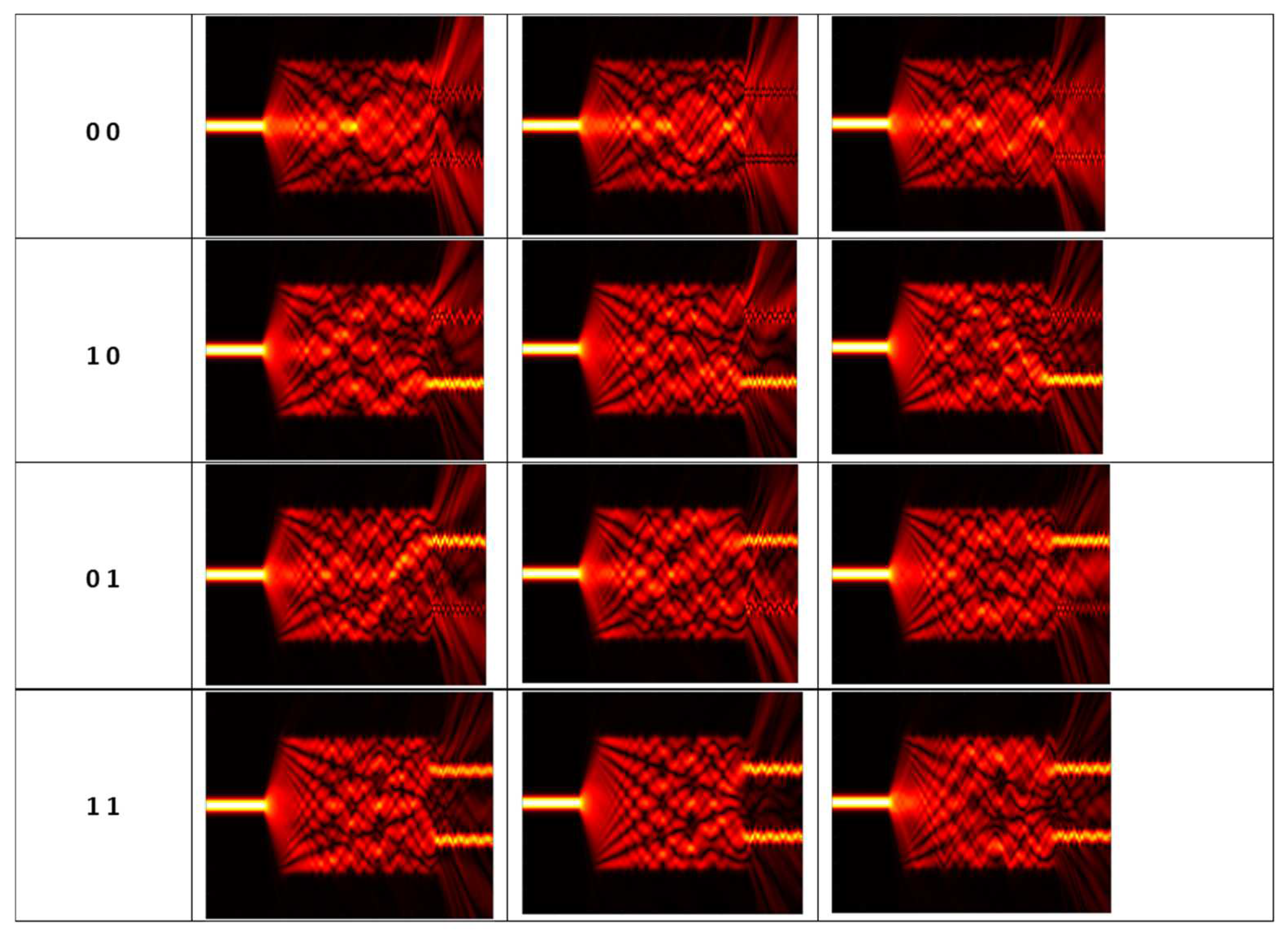
A Python 2.7 script produced a set of about 2 × 10⁵ RSOFT simulation runs, based on a random generation of the MOS distribution. The results have been saved in three different formats: straight numerical, B&W graphical representation of the matrix, and internally generated EM field. Figure 11 reports an example of the three output formats. The classification of the switch function has been operated on the same scheme previously described at the beginning of this section. Figure 12 reports a few samples of the classification result obtained using the images of EM fields. We attribute the digital value 0 or 1 to the output of each channel, depending on the intensity of light. For the analysis carried out, two consequent strategies have been adopted: a machine learning approach from the images and a statistical one from the numerical descriptions. They are detailed in the next section.
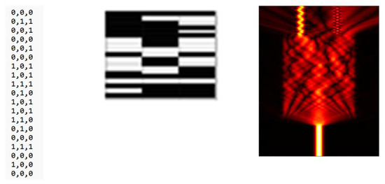
Figure 11.
Simulation output in three different formats: straight numerical, B&W graphical representation of the matrix, and internally generated EM field.
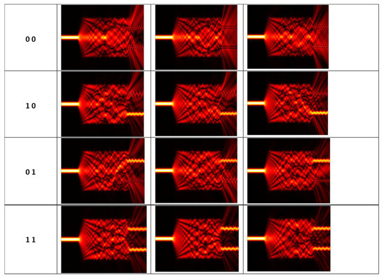
Figure 12.
Examples of the simulation output obtained for the logical output classes.
5. Machine Learning
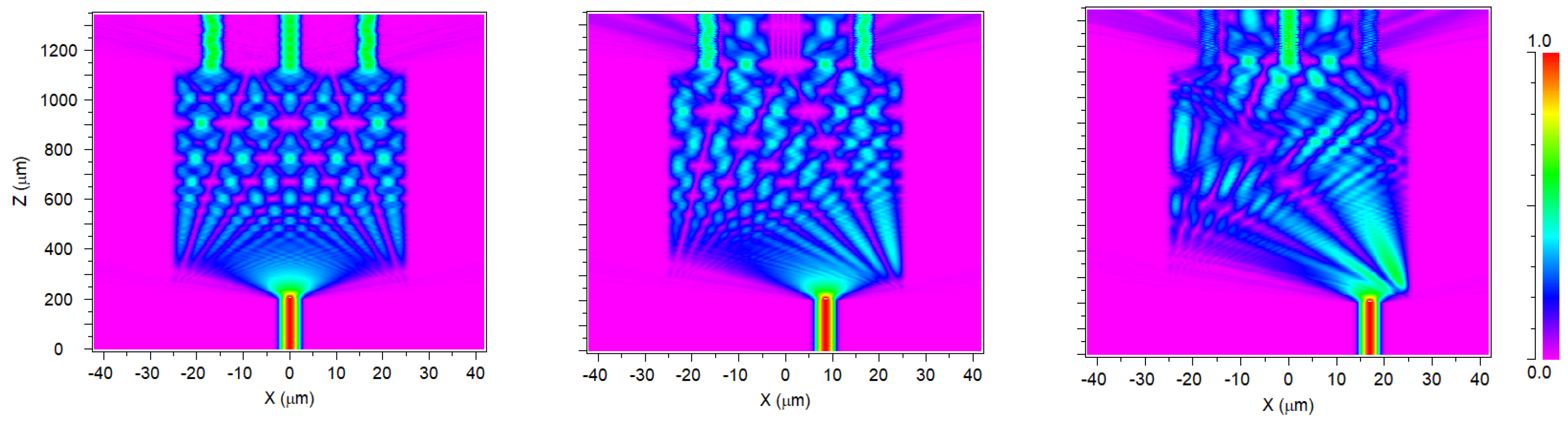
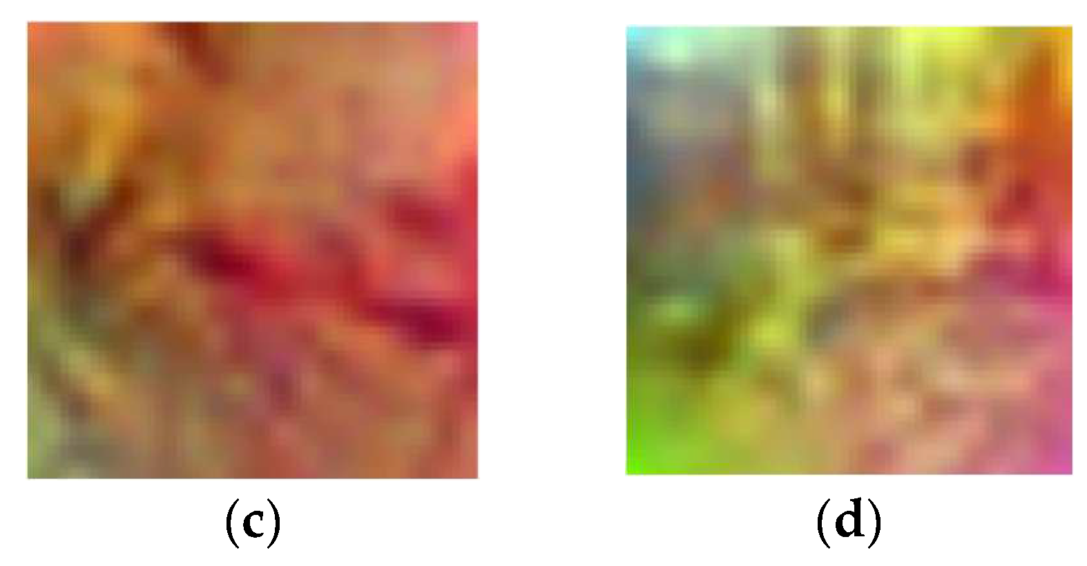
The ML approach for patterns classification according to their generated outputs tries to define a relationship between the features that can be identified in the pictures and the corresponding output they generate. It is a very useful technique when it is assumed that there are also features that cannot be identified by human inspection. In this case, the simulations output in the form of image of internally generated EM field (rightest image in Figure 11) has been used for training of a machine learning network, developed on the Deep Learning Matlab 2023 Toolbox. It is mainly constituted of a sequence of segmentation and convolutions, followed by Normalization and a Rectifying Linear Unit operation to get only positive quantities (for example, ReLU(x) = max(0,x)). Going deeper in the network, the images transformations produce patterns and features that human interpretation cannot explain but are somehow connected to the original images through deterministic operations. For example, one can have patterns like the ones in Figure 13 (a and b, higher level, still geometric features, c. and d., deeper level, lost human visual correspondence and interpretation). It is possible to appreciate in this sequence the progressive blurring effect of the images as a visual characteristic of the ML analysis.
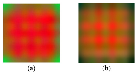

Figure 13.
Examples of output at different levels of the ML network. (a,b), higher level, still geometric features, (c,d) deeper level, lost human visual correspondence and interpretation.
The casual generation of patterns for the input–output determination produced a nonhomogeneous number of samples among the different classes of output, but sufficiently large anyway. The available input set of X analyzed cases has been divided into three subsets: the training, the validation, and the test ones, taking 60%, 20%, and 20% of the data, respectively, a commonly adopted choice.
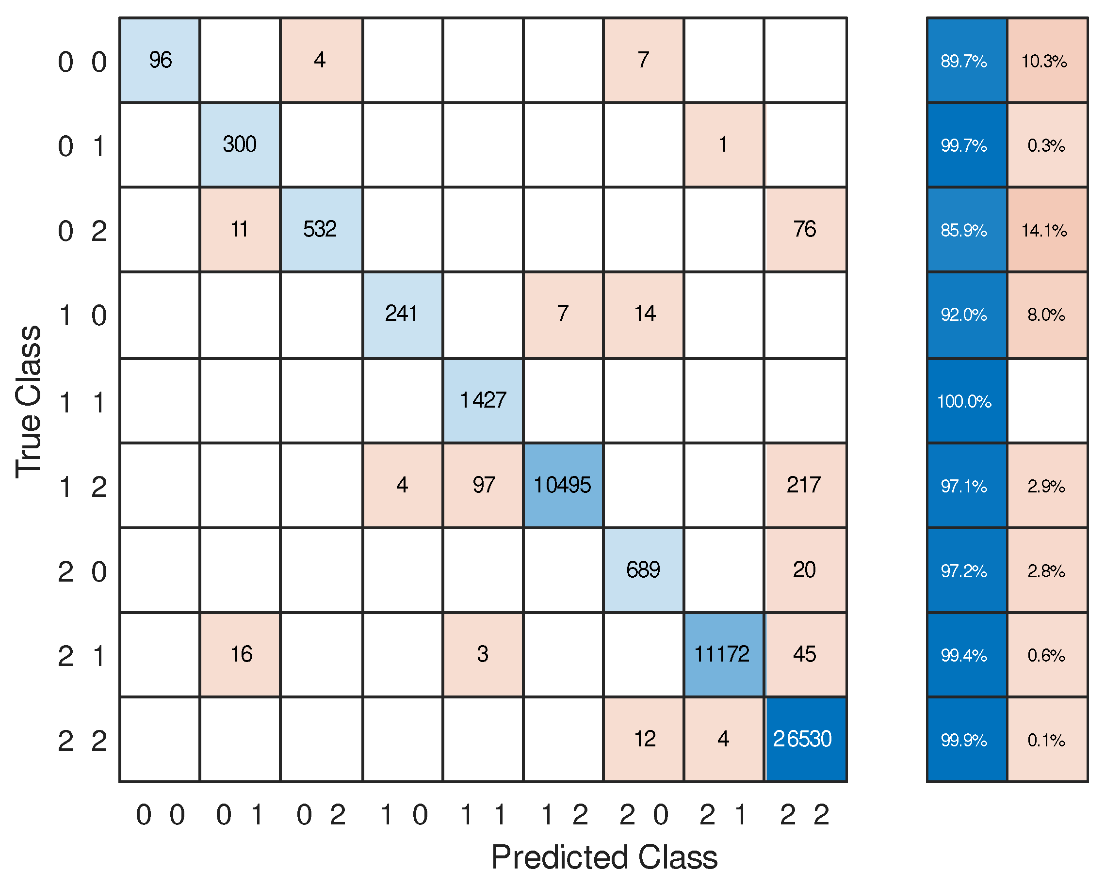
Figure 10 synthetizes the effectiveness of the system identification of the output produced for any given image to be analyzed. It is reported in the form of a confusion matrix for a classification of a 1x2 digital switch output channels, obtained by the previously trained network. It reports, for all the images belonging to each class and given in the vertical axis, which class the trained network associates with, horizontal axis.
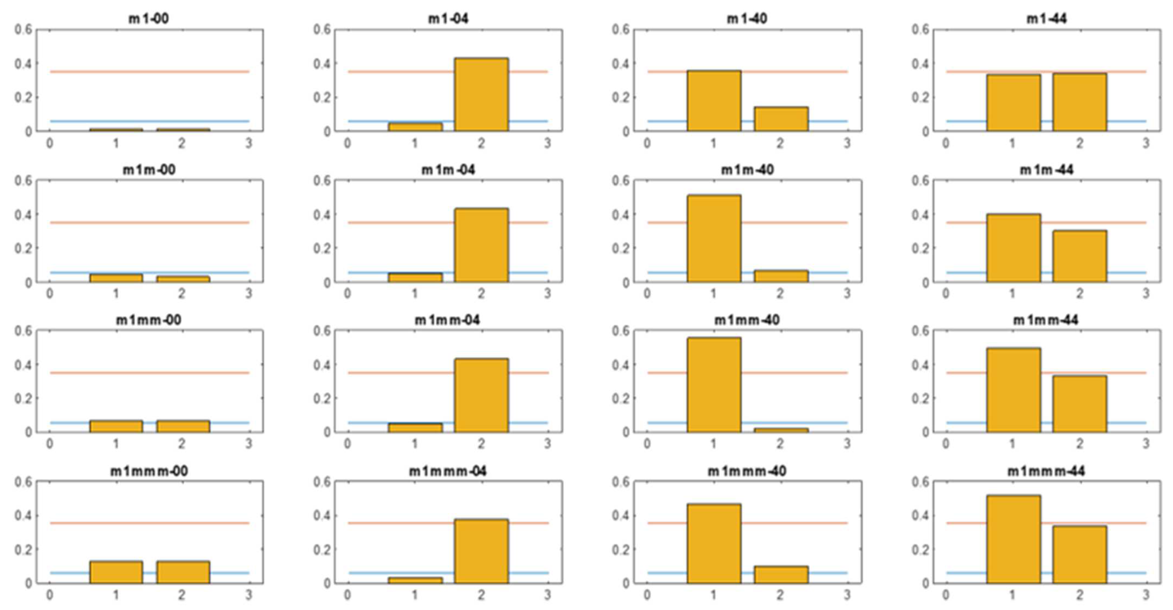
Power in the channel is subdivided in three levels (0, 1, and 2). Precision of the classification is 90%. Accuracy is 97%. 0 should be intended as “light off”, 1 as “light on”, while 2 represents an intermediate value. The four combinations of interest are (0, 0); (1, 0); (1, 0); (1, 1). The values “0” and “1” can be thought as the logical high and logical low in a binary logic family. The presence intermediate value “2”, which is the most commonly obtained, determine the non-usability of the configuration. Normally this result is obtained when we have some light intensity in the output, but not clearly enough do define a logical level.
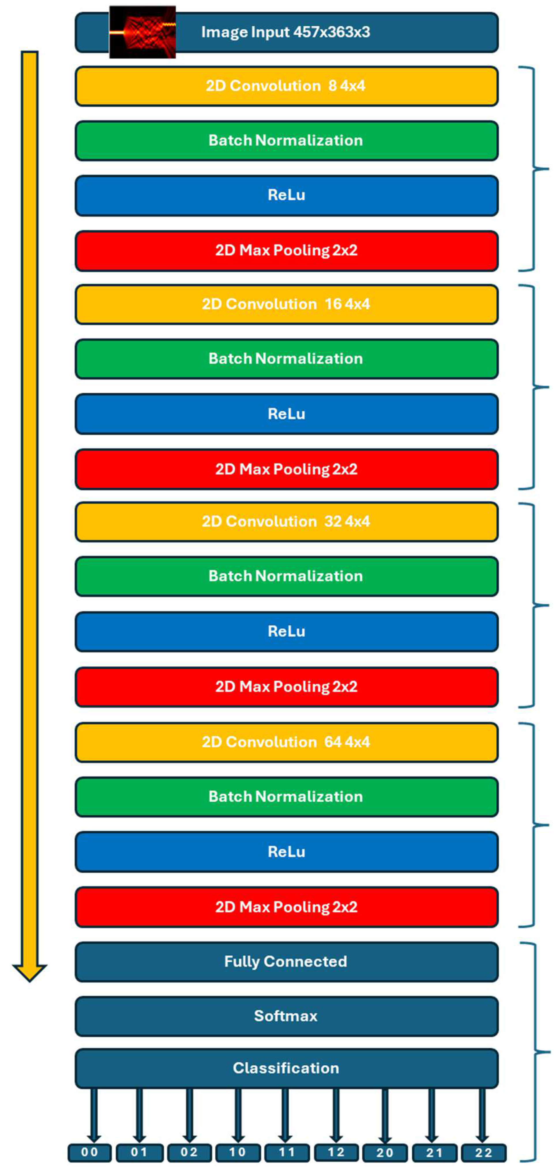
A graphical representation of the network architecture is reported in Figure 14. It is organized over four groups of convolution layers with increasing filters number (from 4 to 64). The confusion matrix obtained after the ML training is reported in Figure 15. The result confirms that the approach can successfully produce an optical reconfigurable digital 1x2 output by controlling the distribution of the refractive index inside a MMI structure, imposed by a MOS active matrix behaving as a reconfigurable metasurface.
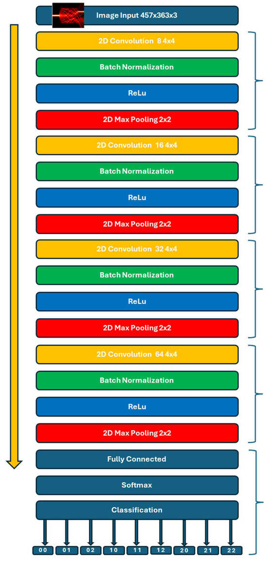
Figure 14.
Network architecture used to classify the output of the 1x2 digital switch.
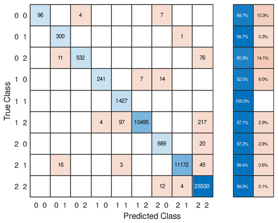
Figure 15.
Confusion matrix for classification of a 1x2 digital switch output channels, obtained by training the system with the images of the field intensities.
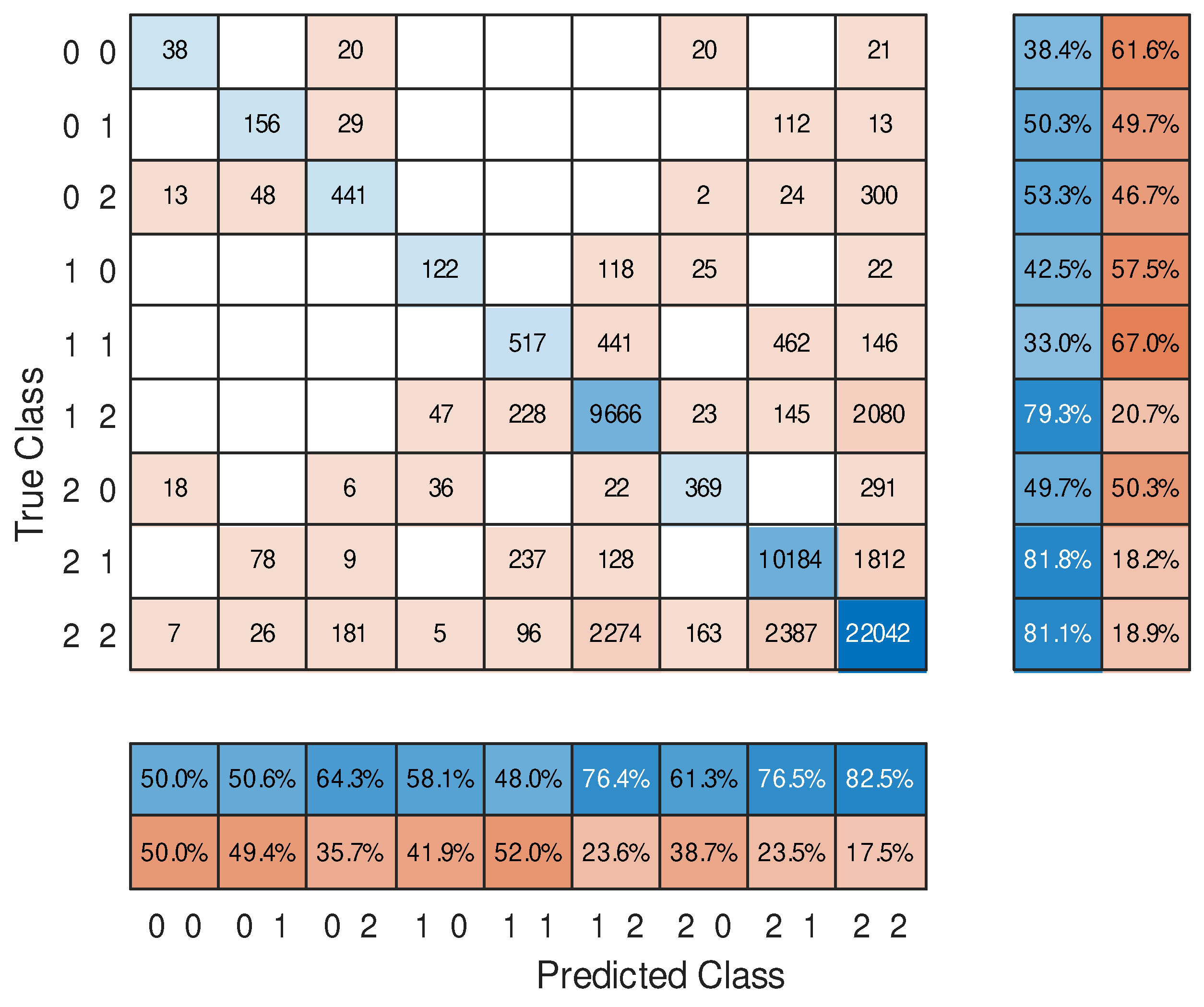
On the other hand, using images like the second kind in Figure 11, B&W pictures representing the binary matrix of activation, the identification of common features characteristics from a geometric figure is not as effective as the use of the simulated internal EM field (third picture in Figure 11); in fact, the confusion matrix obtained in this case after a training phase, depicted in Figure 16, clearly show that it is not so easy to distinguish between consecutive classes; the obtained result has an accuracy of 78% and precision of 56%.
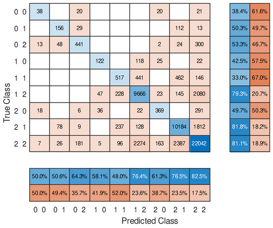
Figure 16.
Confusion matrix for a classification of a 1x2 digital switch output channels, obtained by training the system with the B&W images depicting the binary activation matrix.
This observation confirms that while it is harder to apply a machine learning approach on more complex images, once well trained, the corresponding neural network gains the power to better distinguish the different classes.
However, the binary information yielded by the on/off activation matrix should be sufficient to represent the input map, even without a direct and predictable corresponding output. So, an approach different from an image-based one like in machine learning systems is investigated in the next section.
6. Statistical Analysis
The matrix structure of the device, once seen as an array of activation points, suggests a different approach for the identification and the detection of the characteristic patterns generating each output.
In fact, it is possible to assume that there exists at least one optimal activation pattern for any desired output, and small changes in the optimal pattern (differences in a few activation points, ON instead of OFF and vice versa) produce small changes in the output signals. In this case, given a randomly generated activation array, the closer it is to the (one of) optimal pattern, the more the output is like the exact one. Then, given two activation arrays with comparable output, the differences between their patterns and the optimal one should be small and, consequently, also the differences between their patterns should be small too.
Be the -th array associated with a certain pattern configuration of activated points, the one of (unknown) optimal pattern which best generates the output , and be the error between patterns, for example defined simply as the array
so that each entry , with 0 when the activation point is present in both the patterns and when it is present in only one.
Then, given a set of p patterns which produces outputs comparable with the k-th optimal one , a classical procedure of the least square error computation can be adopted to find the best estimation of the optimal one, defining the mean square error
and computing to minimize . One has
yielding to the classical expression of the average value
Clearly, according to those definitions, each entry of belongs to the continuous interval while entries of the optimal pattern should be 0 or 1. A statistical interpretation of such a result allows one to associate the values of the entries to the probability of the presence of the corresponding activation point in the optimal pattern.
Being the input matrix defined over , possible choices for reliable activation patterns can be obtained assuming a confidential threshold for probability, defining the NxM array with all entries equal to and choosing
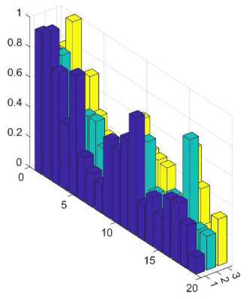
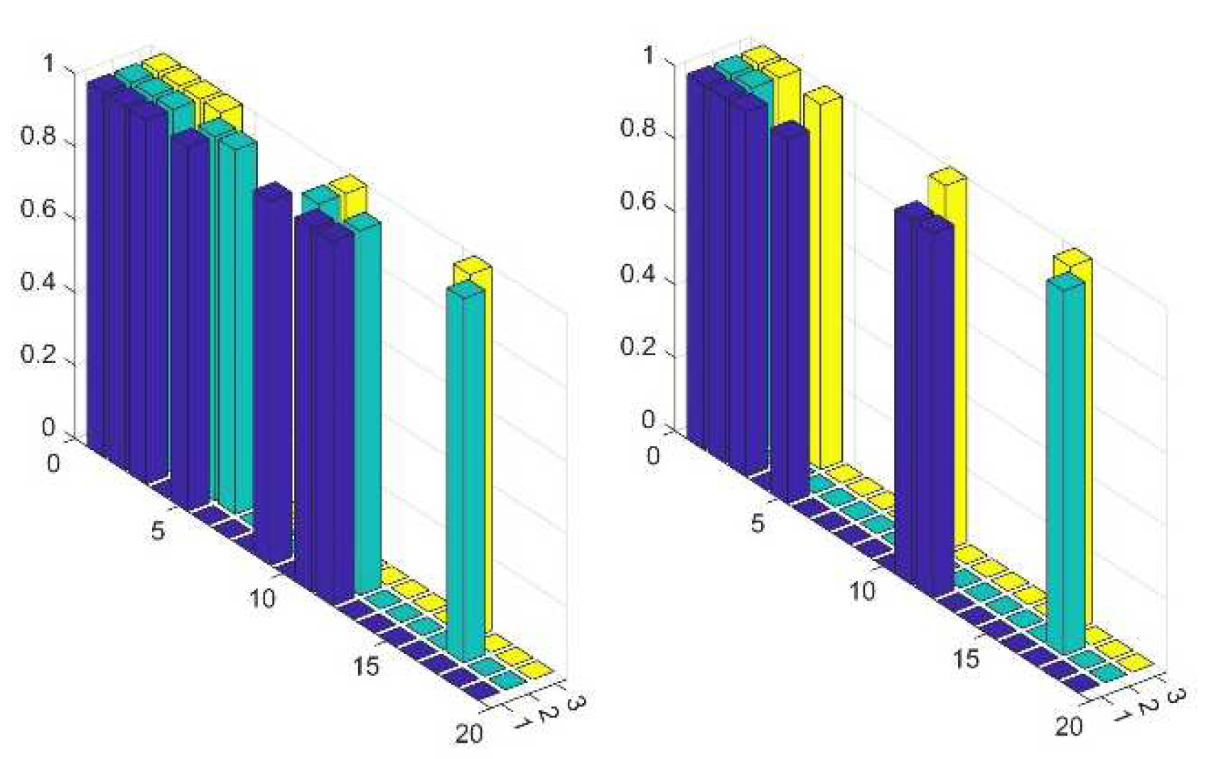
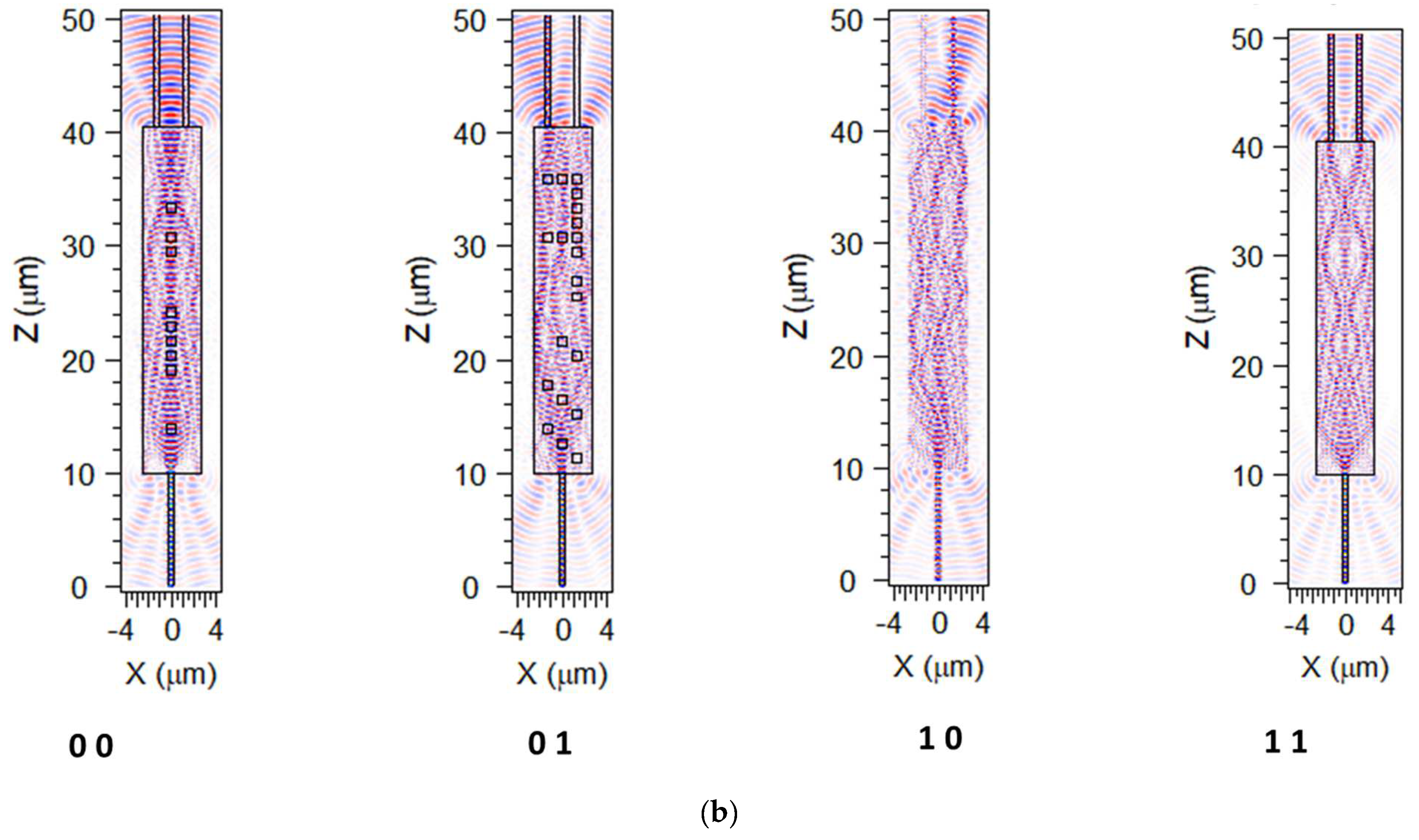
as best approximation of optimal pattern. An example is depicted in Figure 17, where the probability array obtained as the average matrix over all the patterns corresponding to acceptable outputs close to (1,0), , is reported: Correspondingly, the appliable configurations obtained choosing as possible confidence thresholds 0.5 and 0.6 are depicted in Figure 18. All the patterns obtained with such a procedure for all the possible output have been simulated, obtaining very satisfactory results.

Figure 17.
Matrix of probability of activation points for the configuration with output (1, 0).

Figure 18.
Matrix of activation points for output (1, 0) assuming a threshold (left) and (right).
Toward the Optimization of the Metasurfaces
Based on the previously described analysis, a set of optimized configurations has been created for each of the logic classes. Figure 19 reports the results of the output intensities obtained by FDTD simulation of the metaMMI for the different configurations.
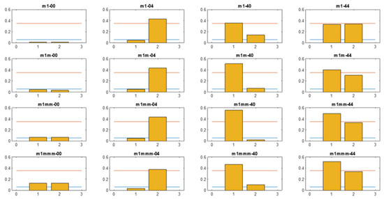
Figure 19.
Figure of Merit for the simulation output obtained by using the optimized MOS arrays. The orange and cyan horizontal line represents the LOW and HIGH logical threshold.
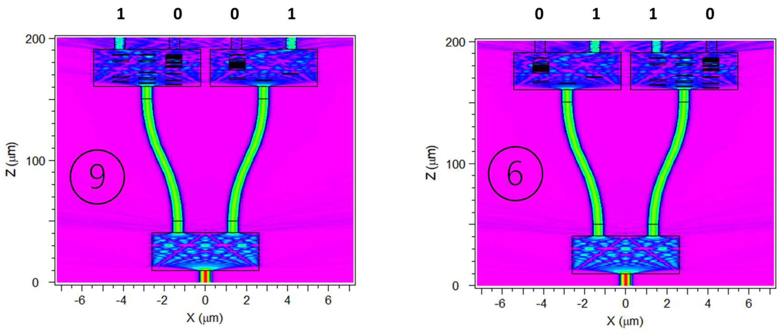
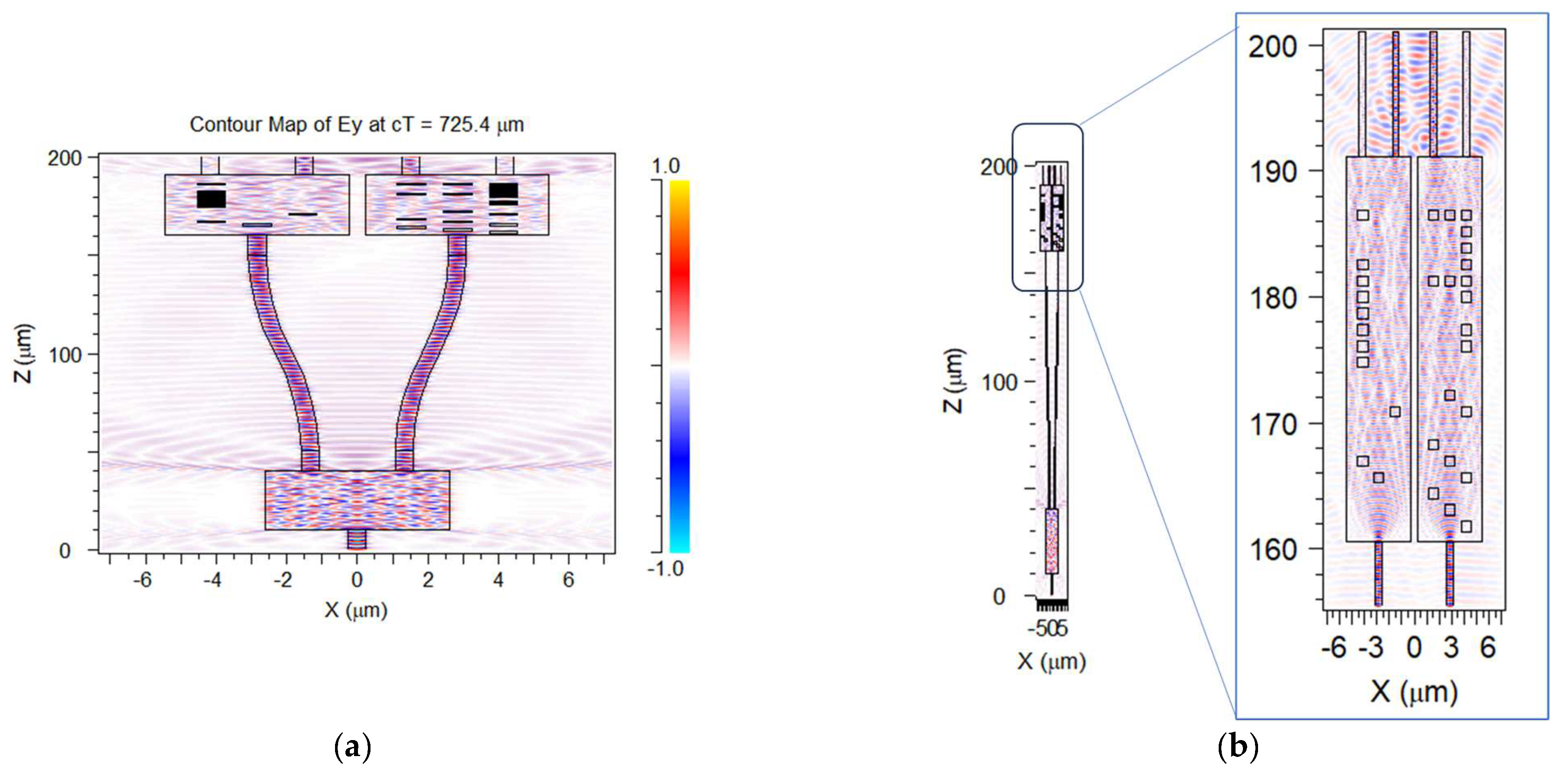
For each class, an example of the results obtained with four different thresholds is reported, together with the HIGH and LOW values used for the classification. The plots report the power value calculated on each output channel. A good agreement was obtained between the results provided by the statistical method and the BPM simulations. The most important consideration is that the method succeeded in creating, separating and isolating the four meaningful configurations from the large number of chaotic layouts leading to intermediate values with no useful meaning. The configurations used for these simulations are not part of the database used for the analysis and are created ex novo. To confirm the effectiveness of the results, additional simulations on the same layouts produced by the FDTD algorithm have been executed. Figure 20 shows the internal field obtained by using the optimized MOS arrays for each of the logical classes obtained by simulating the device by BPM and FDTD algorithms. No significant difference is observed between the results obtained by the different methods and the logic functions are clearly defined for all cases. The output at each channel is satisfactorily controlled by the MOS activation. Obviously, the light intensity in the output is reduced to half of the input, defining some constraints on the Fan-Out limits. The device is compact, with a dimension within the order of few tenths of mm, and multiple combinations of metaMMIs can be arranged for more complex functionalities. In Figure 21, as an example, a cascaded digital switch is demonstrated to write two 4-bit binary numbers: nine and six (1001 and 0110, respectively). The different numbers are obtained through different configurations of the MOS array. As confirmation, in Figure 22 it is reported the 1001 configuration, simulated with the FDTD algorithm. While all the simulation results have been obtained in continuous wave (CW) conditions, the simulation has been also realized with a pulsed light input, demonstrating the correct dynamic operation of the MetaMMI. Two videos about these results are reported as Supplementary Material in Videos S1 and S2.
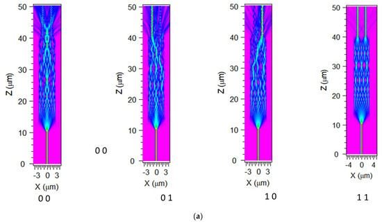

Figure 20.
Internal field obtained by using the optimized MOS arrays for each of the logical class. Simulation obtained by BPM (a) and FDTD (b) algorithms. Different from the other plots, Class 1 0 simulated in FDTD, does not show the device boundaries, for a better visual insight.
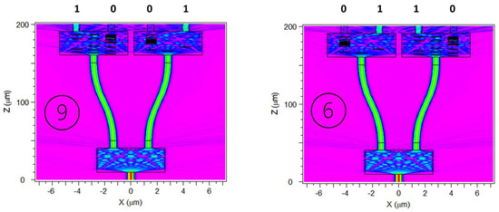
Figure 21.
Internal field of a metaMMI combination used as a cascaded digital switch writing two binary numbers: 9 and 6 (1001 and 0110, respectively). Simulation obtained with BPM method.
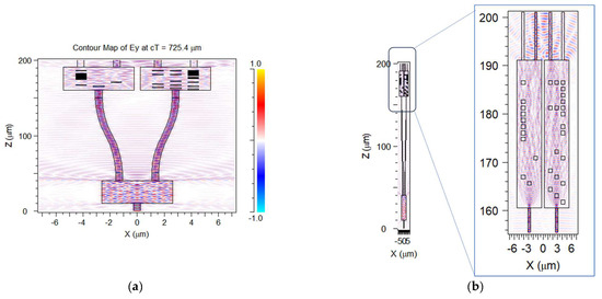
Figure 22.
Internal field of a metaMMI combination used as a cascaded digital switch writing number: 9 (1001) respectively. Simulation obtained with FDTD method. In (a) is reported the overall file distribution. (b) report a zoom on the output port, with respected dimension proportionality.
7. Conclusions
The recent advances in silicon photonic integrated circuits have highlighted the need for a new class of reconfigurable building blocks. In this paper, we have proposed a novel approach, based on a MOS-induced charge accumulation and respective local refractive index modification. As a proof of concept, a 1x2 digital switch has been demonstrated through the application of a machine learning approach for analyzing the MOS matrix configuration. A similar approach can be used for configuring more complex devices, with special attention to a 2x2 reconfigurable optical digital switch, with the potential of being used as the basic building block for programmable photonic integrated circuits. As proof of concept, cascaded switch, operated by a combination of three metaMMIs has been demonstrated in continuous wave and pulsed light input conditions.
Once the method for controlling the reconfigurability of the device is demonstrated, future developments can be elaborated, addressing more complex functionalities, like for example a Nx1 reconfigurable logic gate or a 2x2 switch to be used in programmable PICs. Upscaling the complexity of the photonic circuit by combining a set of metaMMI building blocks will make it possible to design an arbitrary NxM weighted switch. Considering the potential applications of this kind of device as an optical layer for machine learning computation, further investigation is indeed attractive. As reported in the analysis of Section 6, cascade configuration is not an issue. It should be taken into account that by increasing the number of output lines, the signal power will proportionally decrease, leading to a power management limitation that will need to be properly addressed.
Supplementary Materials
The following supporting information can be downloaded at: https://www.mdpi.com/article/10.3390/photonics12030263/s1, Video S1: Time-dependent simulation of a pulsed light input traveling inside a metaMMI (1-1 output) and Video S2: Time-dependent simulation of a pulsed light input traveling inside a metaMMI (0-1 output).
Author Contributions
Conceptualization, A.F. and P.D.G.; methodology, A.F. and P.D.G.; software, A.F. and P.D.G.; validation, A.F.; formal analysis, P.D.G.; resources, A.F. and P.D.G.; data curation, A.F.; writing—original draft preparation, A.F. and P.D.G.; funding acquisition, A.F. and P.D.G. All authors have read and agreed to the published version of the manuscript.
Funding
This research was supported by FCT—Fundação para a Ciência e Tecnologia, through the Portuguese FCT program, Center of Technology and Systems (CTS) UIDB/00066/2020/UIDP/00066/2020, by FCT project ASER-META 2022.07694.PTDC, by project IPL/IDI&CA2024/OPAPIC2D_ISEL and by the University of Roma “la Sapienza” through the Sapienza Visiting Professor Programme 2022.
Institutional Review Board Statement
Not applicable.
Informed Consent Statement
Not applicable.
Data Availability Statement
Data are available upon request.
Acknowledgments
The authors would like to thank Ernesto Velazquez, from Instituto Superior de Engenharia de Lisboa for collaborating on the discussion about the thermo-optical effect.
Conflicts of Interest
The authors declare no conflicts of interest. The funders had no role in the design of the study; in the collection, analyses, or interpretation of data; in the writing of the manuscript; or in the decision to publish the results.
References
- Thomson, D.; Zilkie, A.; Bowers, J.E.; Komljenovic, T.; Reed, G.T.; Vivien, L.; Marris-Morini, D.; Cassan, E.; Virot, L.; Fédéli, J.-M.; et al. Roadmap on silicon photonics. J. Opt. 2016, 18, 073003-1–073003-20. [Google Scholar] [CrossRef]
- Minkenberg, C.; Farrington, N.; Zilkie, A.; Nelson, D.; Lai, C.P.; Brunina, D.; Byrd, J.; Chowdhuri, B.; Kucharewski, N.; Muth, K.; et al. Reimagining datacenter topologies with integrated silicon photonics. J. Opt. Commun. Netw. 2018, 10, B126. [Google Scholar] [CrossRef]
- Margalit, N.; Xiang, C.; Bowers, S.M.; Bjorlin, A.; Blum, R.; Bowers, J.E. Perspective on the future of silicon photonics and electronics. Appl. Phys. Lett. 2021, 118, 220501. [Google Scholar] [CrossRef]
- Shekhar, S.; Bogaerts, W.; Chrostowski, L.; Bowers, J.E.; Hochberg, M.; Soref, R.; Shastri, B.J. Roadmapping the next generation of silicon photonics. Nat. Commun. 2024, 15, 751. [Google Scholar] [CrossRef] [PubMed]
- Soref, R. Tutorial: Integrated-photonic switching structures. APL Photonics 2018, 3, 021101. [Google Scholar] [CrossRef]
- Miscuglio, M.; Sorger, V.J. Photonic tensor cores for machine learning. Appl. Phys. Rev. 2020, 7, 031404. [Google Scholar] [CrossRef]
- Xu, Y.; Huang, J.; Yang, L.; Ma, H.; Yuan, H.; Xie, T.; Yang, J.; Zhang, Z. Inverse-designed ultra-compact high efficiency and low crosstalk optical interconnect based on waveguide crossing and wavelength demultiplexer. Sci. Rep. 2021, 11, 12842. [Google Scholar] [CrossRef]
- Dinsdale, N.J.; Wiecha, P.R.; Delaney, M.; Reynolds, J.; Ebert, M.; Zeimpekis, I.; Thomson, D.J.; Reed, G.T.; Lalanne, P.; Vynck, K.; et al. Deep learning enabled design of complex transmission matrices for universal optical components. ACS Photonics 2021, 8, 283–295. [Google Scholar] [CrossRef]
- Bogaerts, W.; Pérez, D.; Capmany, J.; Miller, D.A.; Poon, J.; Englund, D.; Morichetti, F.; Melloni, A. Programmable photonic circuits. Nature 2020, 586, 207–216. [Google Scholar] [CrossRef]
- Francoy, J.C. General-purpose programmable integrated photonics processors: What things can you do with them? In Proceedings of the SPIE PC13012, Integrated Photonics Platforms III, PC130120J, Strasbourg, France, 19 June 2024; p. 130120. [Google Scholar] [CrossRef]
- Pérez, D.; Gasulla, I.; Mahapatra, P.D.; Capmany, J. Principles, fundamentals, and applications of programmable integrated photonics. Adv. Opt. Photonics 2020, 12, 709–786. [Google Scholar] [CrossRef]
- Beeckman, J.; Bogaerts, W.; Van Iseghem, L.; García, J.P.; Liu, J. Liquid Crystal as Material for Highly Efficient Phase Shifters in Integrated Photonics. In Liquid Crystals Optics and Photonic Devices; SPIE: Bellingham, WA, USA, 2024; p. PC130160H. [Google Scholar]
- Quack, N.; Takabayashi, A.Y.; Sattari, H.; Edinger, P.; Jo, G.; Bleiker, S.J.; Errando-Herranz, C.; Gylfason, K.B.; Niklaus, F.; Khan, U.; et al. Integrated silicon photonic MEMS. Microsyst. Nanoeng. 2023, 9, 27. [Google Scholar] [CrossRef]
- Wang, Q.; Rogers, E.T.; Gholipour, B.; Wang, C.M.; Yuan, G.; Teng, J.; Zheludev, N.I. Optically reconfigurable metasurfaces and photonic devices based on phase change materials. Nat. Photonics 2016, 10, 60–65. [Google Scholar] [CrossRef]
- Nurgali, A.; Nakarmi, B.; Molardi, C.; Ukaegbu, I.A. 4 × 4 bit Programmable Optical Memory Array with Digital Addressing using Micro-Ring Resonators. IEEE Access 2024, 12, 13822–13832. [Google Scholar] [CrossRef]
- Okayama, H.; Matoba, A.; Shibuya, R.; Ishida, T. Optical switch matrix with simplified N*N tree structure. J. Light. Technol. 1989, 7, 1023–1028. [Google Scholar] [CrossRef]
- Silberberg, Y.; Perlmutter, P.; Baran, J.E. Digital Optical Switch. In Optical Fiber Communication Conference; Optica Publishing Group: Washington, DC, USA, 1988; p. ThA3. [Google Scholar]
- Ning, S.; Zhu, H.; Feng, C.; Gu, J.; Jiang, Z.; Ying, Z.; Midkiff, J.; Jain, S.; Hlaing, M.H.; Pan, D.Z.; et al. Photonic-electronic integrated circuits for high-performance computing and ai accelerators. J. Light. Technol. 2024, 42, 7834–7859. [Google Scholar] [CrossRef]
- Chen, T.; Dang, Z.; Ding, Z.; Zhang, Z. Programmable Parallel Optical Logic Gates on a Multimode Waveguide Engine. Photonics 2022, 9, 736. [Google Scholar] [CrossRef]
- Zeng, G.; Zhang, D.; Wang, F.; Wang, X.; Yin, Y. 1 × N All-Logic Optical Switch Based on Polymer Platform Using Multimode Interferometer. Adv. Photonics Res. 2025, 6, 2400118. [Google Scholar] [CrossRef]
- Deng, Z.; Dang, Z.; Chen, T.; Ding, Z.; Zhang, Z. 3-Port beam splitter of arbitrary power ratio enabled by deep learning on a multimode waveguide. Opt. Laser Technol. 2024, 169, 109950. [Google Scholar] [CrossRef]
- Wang, N.; Yan, W.; Qu, Y.; Ma, S.; Li, S.Z.; Qiu, M. Intelligent designs in nanophotonics: From optimization towards inverse creation. PhotoniX 2021, 2, 1–35. [Google Scholar] [CrossRef]
- Meng, Y.; Chen, Y.; Lu, L.; Ding, Y.; Cusano, A.; Fan, J.A.; Hu, Q.; Wang, K.; Xie, Z.; Liu, Z.; et al. Optical meta-waveguides for integrated photonics and beyond. Light Sci. Appl. 2021, 10, 1–44. [Google Scholar] [CrossRef]
- Banerji, S.; Majumder, A.; Hamrick, A.; Menon, R.; Sensale-Rodriguez, B. Ultra-compact integrated photonic devices enabled by machine learning and digital metamaterials. OSA Contin. 2021, 4, 602–607. [Google Scholar] [CrossRef]
- Khatib, O.; Ren, S.; Malof, J.; Padilla, W.J. Deep learning the electromagnetic properties of metamaterials—A comprehensive review. Adv. Funct. Mater. 2021, 31, 2101748. [Google Scholar] [CrossRef]
- Nadell, C.C.; Huang, B.; Malof, J.M.; Padilla, W.J. Deep learning for accelerated all-dielectric metasurface design. Opt. Express 2019, 27, 27523–27535. [Google Scholar] [CrossRef] [PubMed]
- Richter, A.; Matsiusheuski, D.; Polatynski, A.; Duzgol, O.; Sokolov, E.; Koltchanov, I.; Mingaleev, S. Schematic-Driven PIC Design Process Considering Manufacturing Tolerances. In Smart Photonic and Optoelectronic Integrated Circuits XXIII; International Society for Optics and Photonics: Bellingham, WA, USA, 2021; Volume 11690, p. 1169004. [Google Scholar]
- Hillmer, H.; Woidt, C.; Istock, A.; Kobylinskiy, A.; Nguyen, D.T.; Ahmed, N.; Brunner, R.; Kusserow, T. Role of nanoimprint lithography for strongly miniaturized optical spectrometers. Nanomaterials 2021, 11, 164. [Google Scholar] [CrossRef]
- Rabus, D.G.; Sada, C. Sensors. In Integrated Ring Resonators; Springer Series in Optical Sciences; Springer: Cham, Switzerland, 2020; Volume 127. [Google Scholar] [CrossRef]
- Oh, D.K.; Lee, T.; Ko, B.; Badloe, T.; Ok, J.G.; Rho, J. Nanoimprint lithography for high-throughput fabrication of metasurfaces. Front. Optoelectron. 2021, 14, 229–251. [Google Scholar] [CrossRef]
- Zilkie, A.J.; Srinivasan, P.; Trita, A.; Schrans, T.; Yu, G.; Byrd, J.; Nelson, D.A.; Muth, K.; Lerose, D.; Alalusi, M.; et al. Multi-micron silicon photonics platform for highly manufacturable and versatile photonic integrated circuits. IEEE J. Sel. Top. Quantum Electron. 2019, 25, 1–13. [Google Scholar] [CrossRef]
- Trita, A.; Thomas, A.; Rickman, A. CMOS compatible athermal silicon photonic filters based on hydrogenated amorphous silicon. Opt. Express 2022, 30, 19311–19319. [Google Scholar] [CrossRef]
- Schropp, R.E.; Carius, R.; Beaucarne, G. Amorphous silicon, microcrystalline silicon, and thin-film polycrystalline silicon solar cells. MRS Bull. 2007, 32, 219–224. [Google Scholar] [CrossRef]
- Jang, J. Preparation and Properties of Hydrogenated Amorphous Silicon Thin-Film Transistors, Thin Film Tansistors; Kagan, C., Andry, P., Eds.; Marcel Dekker: New York, NY, USA, 2003. [Google Scholar]
- Soref, R.; Bennett, B. Electrooptical effects in silicon. IEEE J. Quantum Electron. 1987, 23, 123–129. [Google Scholar] [CrossRef]
- Rao, S.; Della Corte, F.G. Numerical analysis of electro-optical modulators based on the amorphous silicon technology. J. Light. Technol. 2014, 32, 2399–2407. [Google Scholar] [CrossRef]
- Della Corte, F.G.; Rao, S.; Coppola, G.; Summonte, C. Electro-optical modulation at 1550 nm in an as-deposited hydrogenated amorphous silicon pin waveguiding device. Opt. Express 2011, 19, 2941–2951. [Google Scholar] [CrossRef] [PubMed]
- Reshef, O.; De Leon, I.; Alam, M.Z.; Boyd, R.W. Nonlinear optical effects in epsilon-near-zero media. Nat. Rev. Mater. 2019, 4, 535–551. [Google Scholar] [CrossRef]
- Li, G.; Zhang, S.; Zentgraf, T. Nonlinear photonic metasurfaces. Nat. Rev. Mater. 2017, 2, 17010. [Google Scholar] [CrossRef]
- Amin, R.; George, J.K.; Sun, S.; Ferreira de Lima, T.; Tait, A.N.; Khurgin, J.B.; Miscuglio, M.; Shastri, B.J.; Prucnal, P.R.; El-Ghazawi, T.; et al. ITO-based electro-absorption modulator for photonic neural activation function. APL Mater. 2019, 7, 081112. [Google Scholar] [CrossRef]
- Ye, C.; Liu, K.; Soref, R.A.; Sorger, V.J. A compact plasmonic MOS-based 2 × 2 electro-optic switch. Nanophotonics 2015, 4, 261–268. [Google Scholar] [CrossRef]
- Fantoni, A.; Di Giamberardino, P. A Machine Learning-Based Analysis of a Reconfigurable 1 × 2 Logic Gate Operated Through an Externally-Induced Metamaterial. In Machine Learning in Photonics; SPIE: Bellingham, WA, USA, 2024; Volume 13017, pp. 190–196. [Google Scholar]
- RSOFT Photonic Device Tools. Available online: https://www.synopsys.com/photonic-solutions/rsoft-photonic-device-tools/rsoft-products.html (accessed on 21 December 2024).
- Fernandes, M.; Vieira, M.; Rodrigues, I.; Martins, R. Large area image sensing structures based on a-SiC: H: A dynamic characterization. Sens. Actuators A Phys. 2004, 113, 360–364. [Google Scholar] [CrossRef]
- Vieira, M.A.; Vieira, M.; Louro, P.; Silva, V.; Costa, J.; Fantoni, A. SiC multilayer structures as light controlled photonic active filters. Plasmonics 2013, 8, 63–70. [Google Scholar] [CrossRef]
- Vieira, M.; Fernandes, M.; Fantoni, A.; Louro, P.; Schwarz, R. A new CLSP sensor for Image recognition and color separation. MRS Online Proc. Libr. (OPL) 2002, 715, A3–A4. [Google Scholar] [CrossRef]
- Jacques, M.; Samani, A.; El-Fiky, E.; Patel, D.; Xing, Z.; Plant, D.V. Optimization of thermo-optic phase-shifter design and mitigation of thermal crosstalk on the SOI platform. Opt. Express 2019, 27, 10456–10471. [Google Scholar] [CrossRef]
- Della Corte, F.G.; Montefusco, M.E.; Moretti, L.; Rendina, I.; Rubino, A. Study of the thermo-optic effect in hydrogenated amorphous silicon and hydrogenated amorphous silicon carbide between 300 and 500 K at 1.55 μm. Appl. Phys. Lett. 2001, 79, 168–170. [Google Scholar] [CrossRef]
- Cocorullo, G.; Della Corte, F.G.; Moretti, L.; Rendina, I.; Rubino, A. Measurement of the thermo-optic coefficient of a-Si: H at the wavelength of 1500 nm from room temperature to 200 °C. J. Non-Cryst. Solids 2002, 299, 310–313. [Google Scholar] [CrossRef]
- Della Corte, F.G.; Esposito Montefusco, M.; Moretti, L.; Rendina, I.; Cocorullo, G. Temperature dependence analysis of the thermo-optic effect in silicon by single and double oscillator models. J. Appl. Phys. 2000, 88, 7115–7119. [Google Scholar] [CrossRef]
- Nedeljkovic, M.; Soref, R.; Mashanovich, G.Z. Free-Carrier Electrorefraction and Electroabsorption Modulation Predictions for Silicon Over the 1–14-μm Infrared Wavelength Range. IEEE Photonics J. 2011, 3, 1171–1180. [Google Scholar] [CrossRef]
- Della Corte, F.G.; Rao, S. Use of amorphous silicon for active photonic devices. IEEE Trans. Electron Devices 2013, 60, 1495–1505. [Google Scholar] [CrossRef]
- Bogaerts, W.; Nagarjun, K.P.; Van Iseghem, L.; Chen, X.; Deng, H.; Zand, I.; Zhang, Y.; Liu, Y.; Takabayashi, A.Y.; Sattari, H.; et al. Scaling Programmable Silicon Photonics Circuits. In Silicon Photonics XVIII; SPIE: Bellingham, WA, USA, 2023; Volume 12426, p. 1242601. [Google Scholar]
- Soldano, L.B.; Pennings, E.C. Optical multi-mode interference devices based on self-imaging: Principles and applications. J. Light. Technol. 1995, 13, 615–627. [Google Scholar] [CrossRef]
- Hosseini, A.; Kwong, D.N.; Zhang, Y.; Subbaraman, H.; Xu, X.; Chen, R.T. 1 × N multimode interference beam splitter design techniques for on-chip optical interconnections. IEEE J. Sel. Top. Quantum Electron. 2011, 17, 510–515. [Google Scholar] [CrossRef]
- Lourenço, P.; Fantoni, A.; Costa, J.; Vieira, M. Lithographic mask defects analysis on an MMI 3 dB splitter. Photonics 2019, 6, 118. [Google Scholar] [CrossRef]
- Brotherton, S.D. Introduction to Thin Film Transistors: Physics and Technology of TFTs; Springer Science & Business Media: Berlin, Germany, 2013. [Google Scholar]
- Sun, H.; Qiao, Q.; Guan, Q.; Zhou, G. Silicon Photonic Phase Shifters and Their Applications: A Review. Micromachines 2022, 13, 1509. [Google Scholar] [CrossRef]
- Levi, M.; Chelly, A.; Karsenty, A. A Comprehensive Review of Nanoscale MOS Capacitors Applications in Photonics. Rev. Phys. 2025, 13, 100106. [Google Scholar] [CrossRef]
- Fantoni, A.; Lourenco, P.; Vieira, M. A model for the refractive index of amorphous silicon for FDTD simulation of photonics waveguides. In Proceedings of the 2017 International Conference on Numerical Simulation of Optoelectronic Devices (NUSOD), Copenhagen, Denmark, 24–28 July 2017; IEEE: Piscataway, NJ, USA, 2017; pp. 167–168. [Google Scholar]
- Muller, R.S.; Kamins, T.I. Device Electronics for Integrated Circuits; John Wiley & Sons: Hoboken, NJ, USA, 2002; Chapter 8. [Google Scholar]
- Nedeljković, M. Silicon Photonic Modulators for the Mid-Infrared. Ph.D. Thesis, University of Southampton, Southampton, UK, 2013. [Google Scholar]
- Fantoni, A.; Vieira, M.; Cruz, J.; Schwarz, R.; Martins, R. A two-dimensional numerical simulation of a non-uniformly illuminated amorphous silicon solar cell. J. Phys. D Appl. Phys. 1996, 29, 3154. [Google Scholar] [CrossRef]
- Scarmozzino, R.; Gopinath, A.; Pregla, R.; Helfert, S. Numerical Techniques for Modeling Guided-Wave Photonic Devices. J. Sel. Top. Quantum Electron. 2000, 6, 150. [Google Scholar] [CrossRef]
- Hadley, G.R. Wide-angle beam propagation using Pade approximant operators. Opt. Lett. 1992, 17, 1426. [Google Scholar] [CrossRef] [PubMed]
- Rao, H.; Scarmozzino, R.; Osgood, R.M., Jr. A bidirectional beam propagation method for multiple dielectric interfaces. Photon. Technol. Lett. 1999, 11, 830. [Google Scholar]


Disclaimer/Publisher’s Note: The statements, opinions and data contained in all publications are solely those of the individual author(s) and contributor(s) and not of MDPI and/or the editor(s). MDPI and/or the editor(s) disclaim responsibility for any injury to people or property resulting from any ideas, methods, instructions or products referred to in the content. |
© 2025 by the authors. Licensee MDPI, Basel, Switzerland. This article is an open access article distributed under the terms and conditions of the Creative Commons Attribution (CC BY) license (https://creativecommons.org/licenses/by/4.0/).