High-Performance Optical NOR Gate with SOA-MZI


Abstract
1. Introduction
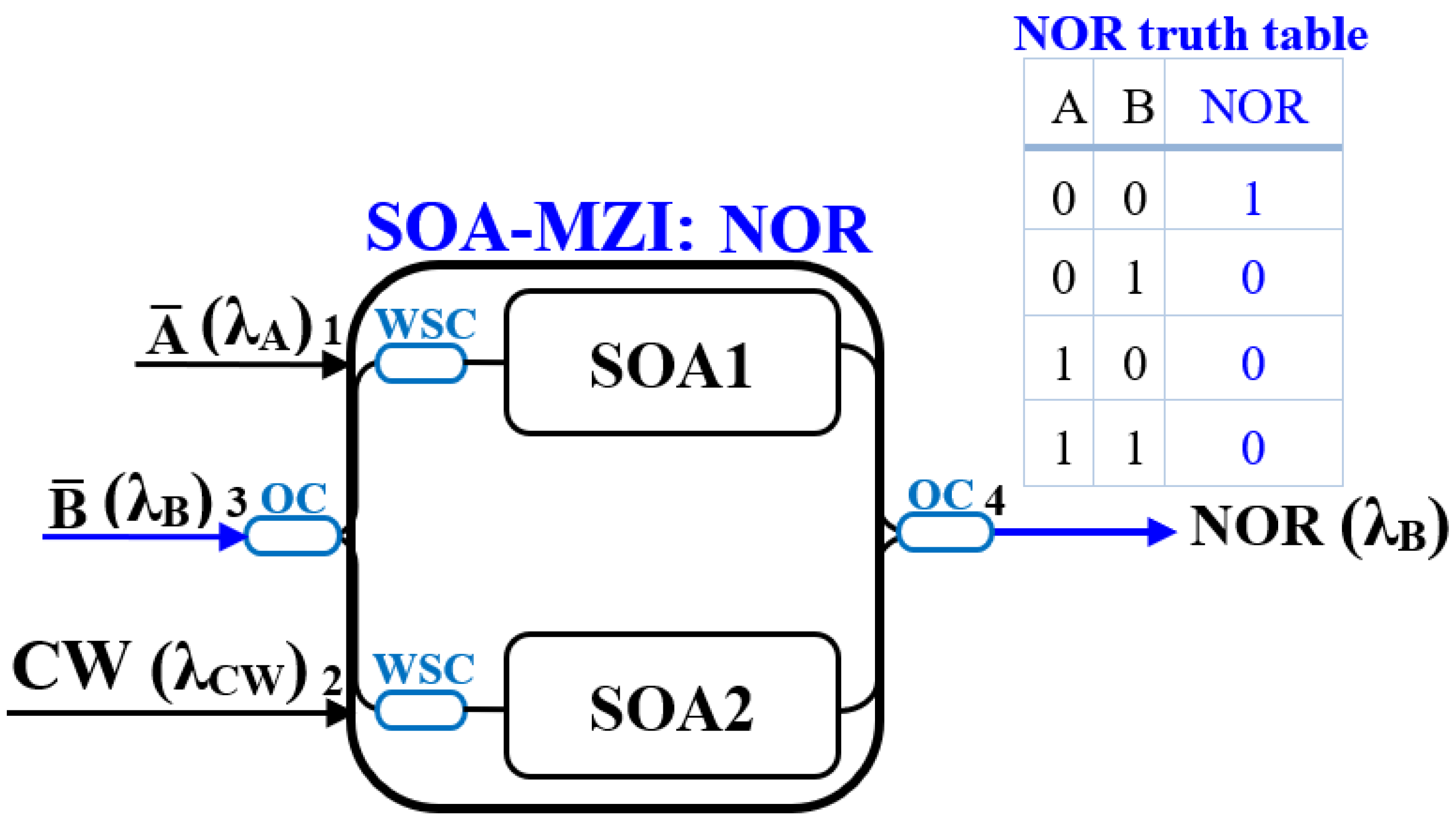
2. NOR Gate
2.1. Operation Principle
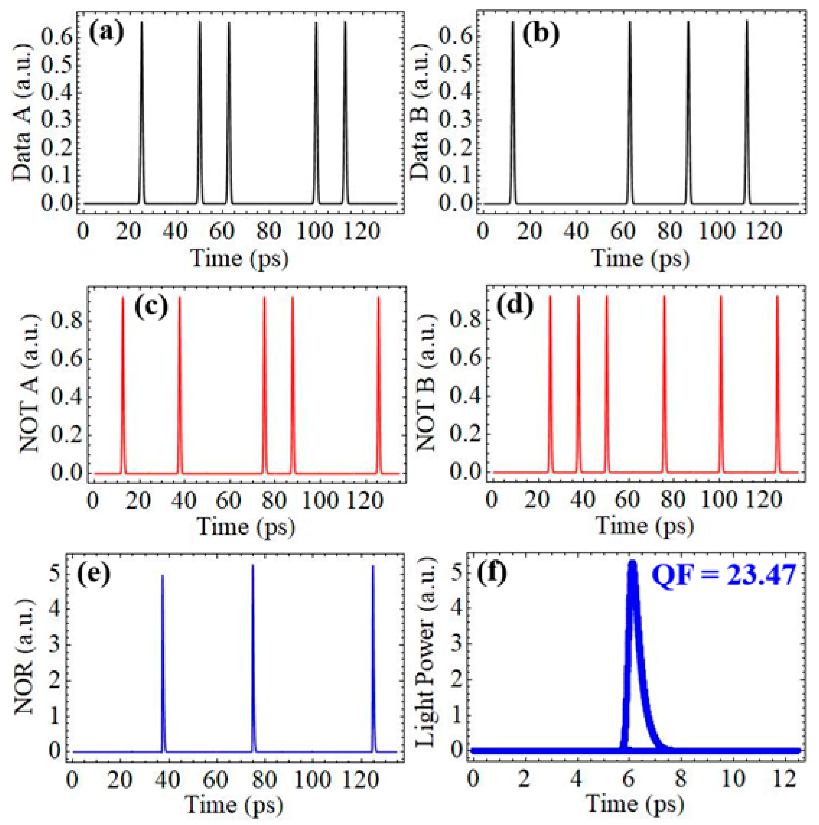
2.2. Numerical Analysis
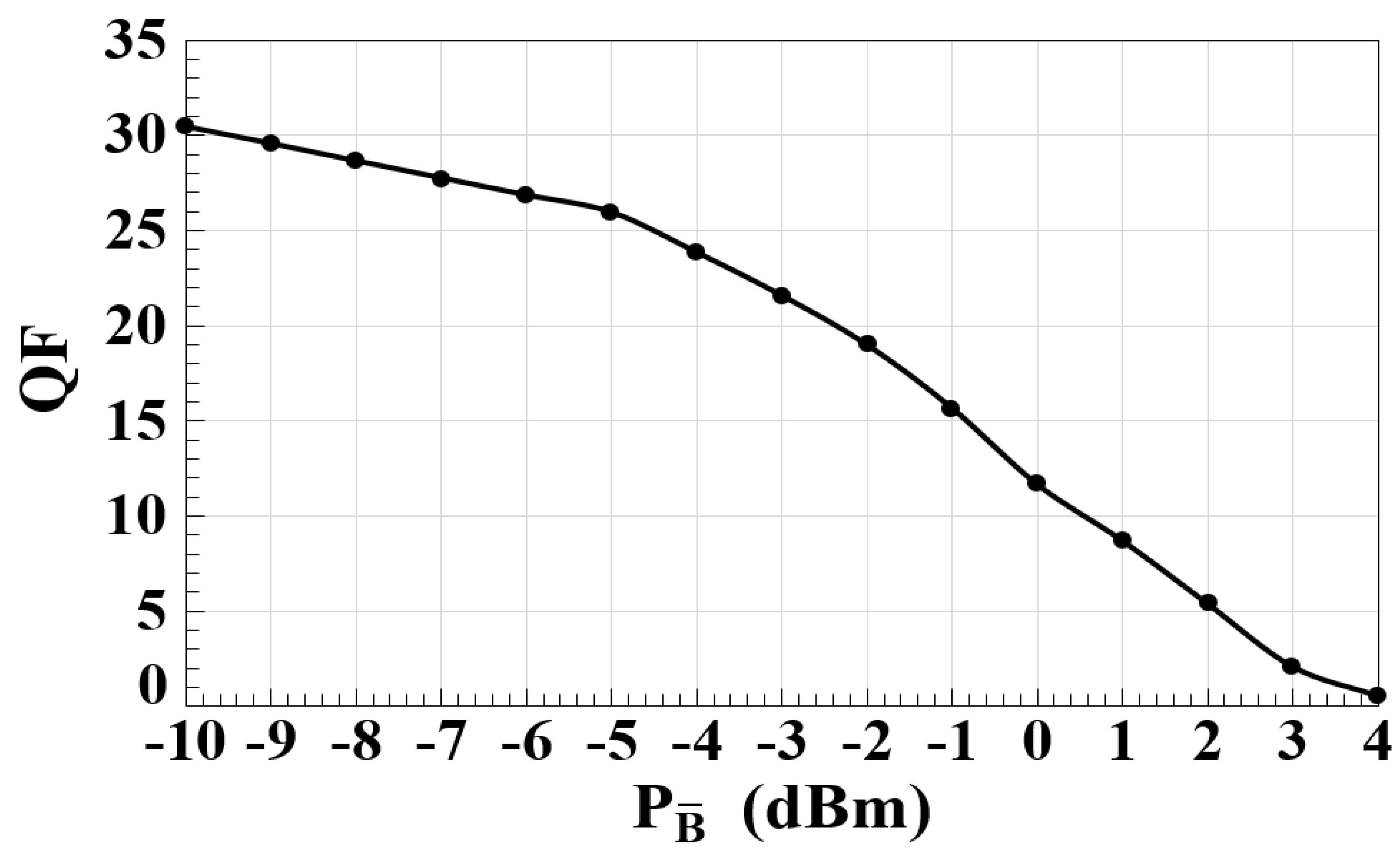
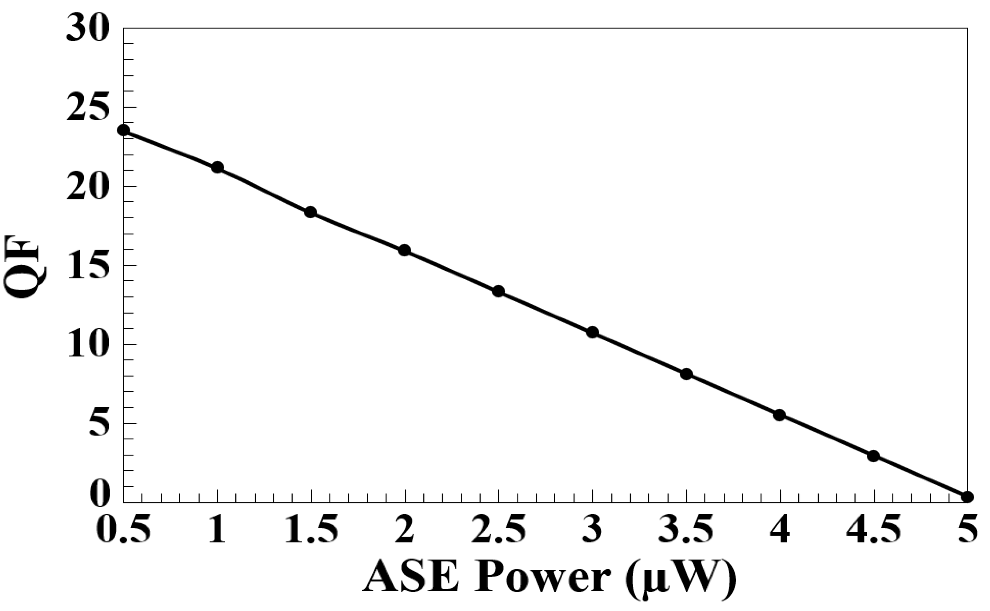
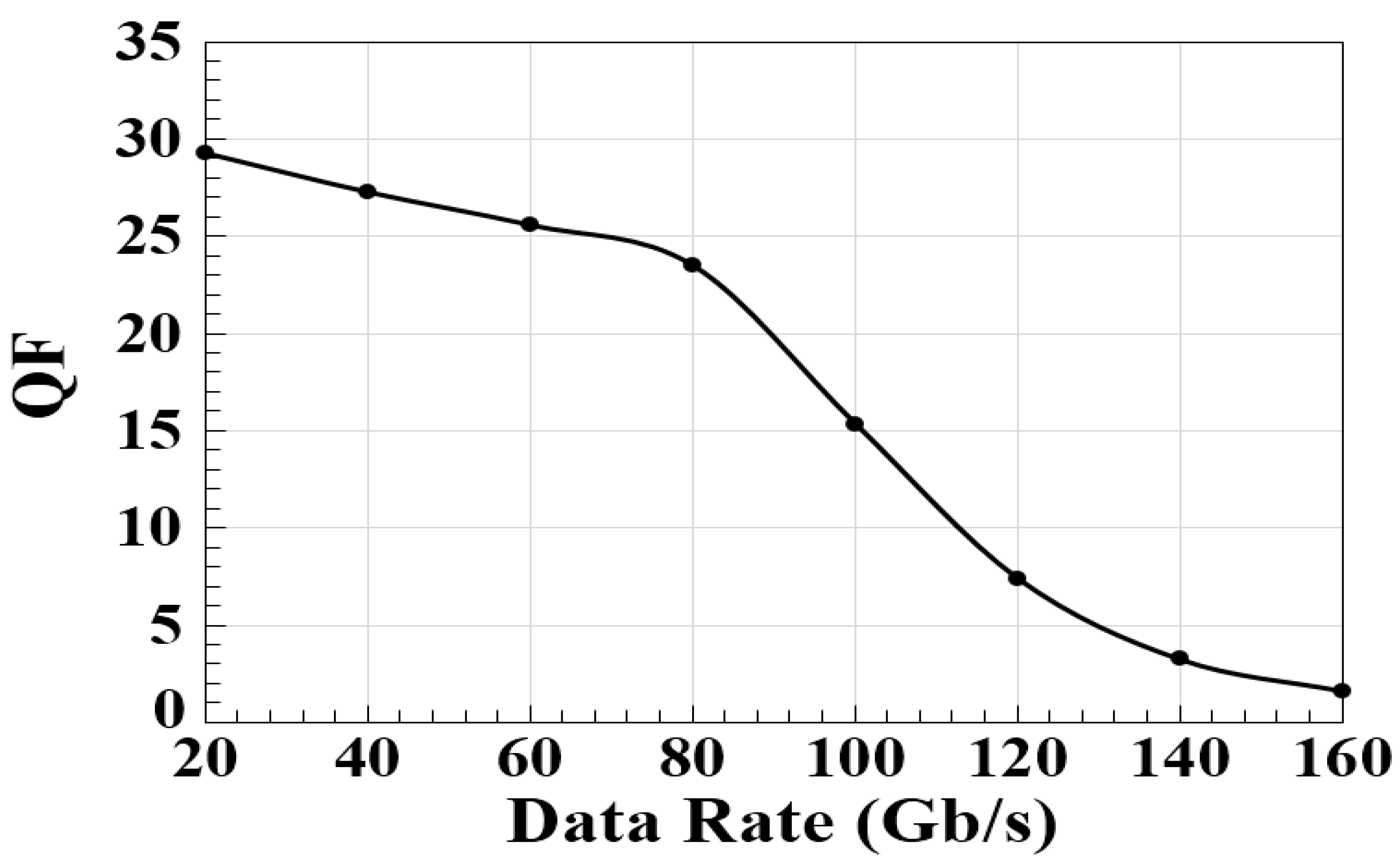
3. Analysis and Discussion
4. Comparison
5. Limitations and Future Work
6. Conclusions
Author Contributions
Funding
Institutional Review Board Statement
Informed Consent Statement
Data Availability Statement
Acknowledgments
Conflicts of Interest
References
- Chan, L.Y.; Qureshi, K.K.; Wai, P.K.A.; Moses, B.; Lui, L.F.K.; Tam, H.Y.; Demokan, M.S. All-optical bit-error monitoring system using cascaded inverted wavelength converter and optical NOR gate. IEEE Photon. Technol. Lett. 2003, 15, 593–595. [Google Scholar] [CrossRef]
- Jung, Y.J.; Son, C.W.; Jhon, Y.M.; Lee, S.; Park, N. One-level simplification method for all-optical combinational logic circuits. IEEE Photon. Technol. Lett. 2008, 20, 800–802. [Google Scholar] [CrossRef]
- Xu, J.; Zhang, X.; Dong, J.; Liu, D.; Huang, D. Simultaneous all-optical AND and NOR gates for NRZ differential phase-shift-keying signals. IEEE Photon. Technol. Lett. 2008, 20, 596–598. [Google Scholar] [CrossRef]
- Dutta, N.K.; Wang, Q. Semiconductor Optical Amplifiers, 2nd ed.; World Scientific: Singapore, 2013. [Google Scholar]
- Taraphdar, C.; Chattopadhyay, T.; Roy, J.N. Mach–Zehnder interferometer-based all-optical reversible logic gate. Opt. Laser Technol. 2010, 42, 249–259. [Google Scholar] [CrossRef]
- Roy, J.N. Mach–Zehnder interferometer-based tree architecture for all-optical logic and arithmetic operations. Optik 2009, 120, 318–324. [Google Scholar] [CrossRef]
- Vadukanathan, A.; Suyambragasam, G.; Sivaraj, P.; Kasiviswanathan, M.M.S. Simulation of all-optical NOR gate design with improved extinction ratio using semiconductor optical amplifier. Microw. Opt. Technol. Lett. 2024, 66, e33993. [Google Scholar] [CrossRef]
- Han, B.; Liu, Y. All-optical reconfigurable non-inverted logic gates with a single semiconductor optical amplifier. AIP Adv. 2019, 9, 015007. [Google Scholar] [CrossRef]
- Kotb, A.; Zoiros, K.E.; Guo, C. All-optical XOR, NOR, and NAND logic functions with parallel semiconductor optical amplifier-based Mach-Zehnder interferometer modules. Opt. Laser Technol. 2018, 108, 426–433. [Google Scholar] [CrossRef]
- Chen, X.; Huo, L.; Zhao, Z.; Zhuang, L.; Lou, C. Study on 100-Gb/s reconfigurable all-optical logic gates using a single semiconductor optical amplifier. Opt. Express 2016, 24, 30245–30253. [Google Scholar] [CrossRef]
- El-Saeed, E.M.; Abd El-Aziz, A.; Fayed, H.A.; Aly, M.H. Optical logic gates based on semiconductor optical amplifier Mach–Zehnder interferometer: Design and simulation. Opt. Eng. 2016, 55, 025104. [Google Scholar] [CrossRef]
- Singh, P.; Tripathi, D.K.; Dixit, H.K. Designs of all-optical NOR gates using SOA based MZI. Optik 2014, 125, 4437–4440. [Google Scholar] [CrossRef]
- Kotb, A.; Ma, S.; Chen, Z.; Dutta, N.K.; Said, G. Effect of amplified spontaneous emission on semiconductor optical amplifier-based all-optical logic. Opt. Commun. 2011, 284, 5798–5803. [Google Scholar] [CrossRef]
- Dong, J.; Zhang, X.; Xu, J.; Huang, D. 40 Gb/s all-optical logic NOR and OR gates using a semiconductor optical amplifier: Experimental demonstration and theoretical analysis. Opt. Commun. 2008, 281, 1710–1715. [Google Scholar] [CrossRef]
- Sun, H.; Chen, Z.; Ma, S.; Dutta, N.K. All-optical logic NOR gate using SOA-based Mach-Zehnder interferometer. In Proceedings of the Active and Passive Optical Components for Communications VII, Optics East, Boston, MA, USA, 10 September 2007; Volume 6775. [Google Scholar]
- Sharaiha, A.; Topomondzo, J.; Morel, P. All-optical logic AND-NOR gates with three inputs based on cross-gain modulation in a semiconductor optical amplifier. Opt. Commun. 2006, 265, 322–325. [Google Scholar] [CrossRef]
- Kim, J.Y.; Kang, J.M.; Kim, T.Y.; Han, S.K. All-optical multiple logic gates with XOR, NOR, OR, and NAND function using parallel SOA-MZI structures: Theory and experiment. J. Lightwave Technol. 2006, 24, 3392–3399. [Google Scholar]
- Kim, J.Y.; Kang, J.M.; Kim, T.Y.; Han, S.K. 10 Gbits all-optical composite logic gates with XOR, NOR, OR, and NAND functions using SOA-MZI structures. Electron. Lett. 2006, 42, 303–307. [Google Scholar] [CrossRef]
- Xu, J.; Zhang, X.; Liu, D.; Huang, D. Ultrafast all-optical NOR gate based on semiconductor optical amplifier and fiber delay interferometer. Opt. Express 2006, 14, 10708–10714. [Google Scholar] [CrossRef]
- Zhao, C.; Zhang, X.; Liu, H.; Liu, D.; Huang, D. Tunable all-optical NOR gate at 10 Gb/s based on SOA fiber ring laser. Opt. Express 2005, 13, 2793–2798. [Google Scholar] [CrossRef]
- Kim, J.H.; Kim, Y.I.; Byun, Y.T.; Jhon, Y.M.; Lee, S.; Kim, S.H.; Woo, D.H. All-optical logic gates using semiconductor optical-amplifier-based devices and their applications. J. Korean Phys. Soc. 2004, 45, 1158–1161. [Google Scholar]
- Byun, Y.T.; Kim, J.H.; Jhon, Y.M.; Lee, S.; Woo, D.H.; Kim, S.H. High-speed all-optical NOR gate using semiconductor optical amplifier. In Proceedings of the 2003 Conference on Lasers and Electro-Optics Europe (CLEO/Europe 2003) (IEEE Cat. No.03TH8666), Munich, Germany, 22–27 June 2003. [Google Scholar]
- Prakash, S.; Joseph, S.; Kishore, D.; Devi, Y. Stochastic Computing Solutions: Challenges and Applications. Adv. Technol. Digit. Eng. 2023, 10, 3233. [Google Scholar]
- López-Magaña, C.; Rivera, J.; Ortega-Cisneros, S.; Sandoval-Ibarra, F.; Del Valle, J.L. A Reduced Hardware SNG for Stochastic Computing. Electronics 2023, 12, 3383. [Google Scholar] [CrossRef]
- Cao, X.Y.; Li, B.H.; Wang, Y.; Fu, Y.; Yin, H.L.; Chen, Z.B. Experimental Quantum E-Commerce. Sci. Adv. 2024, 10, eadk3258. [Google Scholar] [CrossRef] [PubMed]
- Zhou, M.G.; Liu, Z.P.; Yin, H.L.; Li, C.L.; Xu, T.K.; Chen, Z.B. Quantum Neural Network for Quantum Neural Computing. Research 2023, 6, 0134. [Google Scholar] [CrossRef] [PubMed]
- Bartlett, B.; Fan, S. Universal programmable photonic architecture for quantum information processing. Phys. Rev. A 2020, 101, 042319. [Google Scholar] [CrossRef]
- Choure, K.K.; Saharia, A.; Mudgal, N.; Pandey, R.; Prajapat, M.; Maddila, R.K.; Tiwari, M.; Singh, G. Implementation of all-optical single qubit gates using Si3N4-based micro ring resonator. Opt. Laser Technol. 2024, 170, 110263. [Google Scholar] [CrossRef]
- Kotb, A.; Guo, C. All-optical OR and NOR gates using quantum-dot semiconductor optical amplifiers-assisted turbo-switched Mach-Zehnder interferometer and serially delayed interferometer at 1 Tb/s. Optik 2020, 218, 164879. [Google Scholar] [CrossRef]
- Kotb, A. 1 Tb/s high-quality factor NOR gate based on quantum-dot semiconductor optical amplifier. Opt. Quant. Electron. 2013, 45, 1258–1268. [Google Scholar] [CrossRef]
- Dimitriadou, E.; Zoiros, K.E. On the design of reconfigurable ultrafast all-optical NOR and NAND gates using a single quantum-dot semiconductor optical amplifier-based Mach-Zehnder interferometer. J. Opt. 2012, 14, 105401. [Google Scholar] [CrossRef]
- Dimitriadou, E.; Zoiros, K.E. Proposal for all-optical NOR gate using single quantum-dot semiconductor optical amplifier-based Mach-Zehnder interferometer. Opt. Commun. 2012, 285, 1710–1716. [Google Scholar] [CrossRef]
- Kotb, A.; Zoiros, K.E.; Li, W. Computational investigation of all-optical NOR logic operation using carrier reservoir semiconductor optical amplifiers at 120 Gb/s. Opt. Quant. Electron. 2022, 54, 827. [Google Scholar] [CrossRef]
- Mukherjee, K.; Maji, K.; Raja, A.; Mandal, M.K. All-optical soliton based universal logic NOR utilizing a single reflective semiconductor optical amplifier (RSOA). Photon. Netw. Commun. 2022, 43, 101–108. [Google Scholar] [CrossRef]
- Kotb, A.; Guo, C. Reflective semiconductor optical amplifiers-based all-optical NOR and XNOR logic gates at 120 Gb/s. J. Mod. Opt. 2020, 67, 1424–1435. [Google Scholar] [CrossRef]
- Kotb, A.; Guo, C. Numerical modeling of photonic crystal semiconductor optical amplifiers-based 160 Gb/s all-optical NOR and XNOR logic gates. Opt. Quant. Electron. 2020, 52, 1–17. [Google Scholar] [CrossRef]
- Kotb, A. Simulation of all-optical logic NOR gate based on two-photon absorption with semiconductor optical amplifier-assisted Mach-Zehnder interferometer with the effect of amplified spontaneous emission. J. Korean Phys. Soc. 2015, 66, 1593–1598. [Google Scholar] [CrossRef]
- Kumar, A.; Kumar, S.; Raghuwanshi, S.K. Implementation of All-Optical Logic Gate Using SOA-MZI Structures. STM J. 2013, 3, 13–21. [Google Scholar]
- Zhang, X.; Dutta, N.K. Effects of two-photon absorption on all optical logic operation based on quantum-dot semiconductor optical amplifiers. J. Mod. Opt. 2018, 65, 166–173. [Google Scholar] [CrossRef]
- Contestabile, G.; Maruta, A.; Sekiguchi, S.; Morito, K.; Sugawara, M.; Kitayama, K. Cross-gain modulation in quantum-dot SOA at 1550 nm. IEEE J. Quant. Electron. 2010, 46, 1696–1703. [Google Scholar] [CrossRef]
- Sobhanan, A.; Anthur, A.; O’Duill, S.; Pelusi, M.; Namiki, S.; Barry, L.; Venkitesh, D.; Agrawal, G.P. Semiconductor optical amplifiers: Recent advances and applications. Adv. Opt. Photon. 2022, 14, 571–651. [Google Scholar] [CrossRef]
- Yamada, M. Noise in semiconductor optical amplifiers (SOA). In Proceedings of the 2016 IEEE 6th International Conference on Photonics (ICP), Kuching, Malaysia, 11–13 March 2016; pp. 1–5. [Google Scholar]
- de Melo, A.M.; Petermann, K. On the amplified spontaneous emission noise modeling of semiconductor optical amplifiers. Opt. Commun. 2008, 281, 4598–4605. [Google Scholar] [CrossRef]


| Symbol | Definition | Value | Unit |
|---|---|---|---|
| E0 | Pulse energy | 0.07 | pJ |
| τFWHM | Pulse width | 1 | ps |
| T | Bit period | 12.5 | ps |
| n | PRBS length | 127 | - |
| wavelength | 1549.32 | nm | |
| wavelength | 1563.9 | nm | |
| λCW | CW wavelength | 1555.75 | nm |
| input power | −3.96 | dBm | |
| input power | −3.69 | dBm | |
| PCW | CW input power | −2.67 | dBm |
| I | Injection current | 300 | mA |
| Psat | Saturation power | 30 | mW |
| τc | Carrier lifetime | 200 | ps |
| α | α-factor | 5 | - |
| αCH | CH linewidth enhancement factor | 1 | - |
| αSHB | SHB linewidth enhancement factor | 0 | - |
| εCH | CH nonlinear gain suppression factor | 0.1 | W−1 |
| εSHB | SHB nonlinear gain suppression factor | 0.1 | W−1 |
| τCH | Temperature relaxation rate | 0.3 | ps |
| τSHB | Carrier-carrier scattering rate | 0.1 | ps |
| Γ | Confinement factor | 0.3 | - |
| α | Differential gain | 10−20 | m2 |
| Ntr | Transparency carrier density | 1024 | m−3 |
| L | Active region length | 500 | μm |
| d | Active region thickness | 0.3 | μm |
| w | Active region width | 3 | μm |
| G0 | Unsaturated power gain | 30 | dB |
| Nsp | Spontaneous emission factor | 2 | - |
| B0 | Optical bandwidth | 3 | nm |
| Ref. | Scheme | Speed (Gb/s) | Methodology | Metric |
|---|---|---|---|---|
| [3] | SOA-DI | 20 | Experimental | ER = 10 dB |
| [7] | SOA | 40 | Simulation | ER = 20.285 dB |
| [9] | SOA-MZIs | 80 | Simulation | QF = 15.4 |
| [10] | SOA | 100 | Experimental | QF = 7.4 |
| [11] | SOA-MZI | 10 | Simulation | QF = 6.9 |
| [12] | SOA-MZI | 10 | Experimental | QF = 5.86 |
| [13] | SOA-MZI | 80 | Simulation | QF = 8.2 |
| [14] | SOA | 40 | Experimental | QF = 6.5 |
| [15] | SOA-MZI | 40 | Simulation | QF = 10 |
| [16] | SOA | 1.25 | Experimental | ER = 8.5 dB |
| [17] | SOA-MZI | 10 | Experimental | ER = 15 dB |
| [18] | SOAs-MZIs | 10 | Experimental | ER = 15 dB |
| [19] | SOA-DI | 40 | Experimental | ER = 10 dB |
| [20] | SOA | 10 | Experimental | ER = 10.3 dB |
| [29] | QD-SOA-MZI | 1000 | Simulation | QF = 14.3 |
| [29] | QD-SOA-MZI-DI | 1000 | Simulation | QF = 21 |
| [30] | QD-SOA-MZI | 250 | Simulation | QF = 17.3 |
| [31] | QD-SOA-MZI | 160 | Simulation | ER = 10 dB |
| [32] | QD-SOA-MZI | 160 | Simulation | ER = 12 dB |
| [33] | CR-SOA-MZI | 120 | Simulation | QF = 14 |
| [34] | R-SOA | 200 | Simulation | ER = 14 dB |
| [35] | R-SOA-MZI | 120 | Simulation | QF = 17.5 |
| [36] | PhC-SOA-MZI | 160 | Simulation | QF = 21.1 |
| [37] | SOA-MZI-TPA | 250 | Simulation | QF = 12 |
| This work | SOA-MZI | 80 | Simulation | QF = 23.47 |
Disclaimer/Publisher’s Note: The statements, opinions and data contained in all publications are solely those of the individual author(s) and contributor(s) and not of MDPI and/or the editor(s). MDPI and/or the editor(s) disclaim responsibility for any injury to people or property resulting from any ideas, methods, instructions or products referred to in the content. |
© 2025 by the authors. Licensee MDPI, Basel, Switzerland. This article is an open access article distributed under the terms and conditions of the Creative Commons Attribution (CC BY) license (https://creativecommons.org/licenses/by/4.0/).
Share and Cite
Kotb, A.; Zoiros, K.E.; Chen, W. High-Performance Optical NOR Gate with SOA-MZI. Photonics 2025, 12, 179. https://doi.org/10.3390/photonics12030179
Kotb A, Zoiros KE, Chen W. High-Performance Optical NOR Gate with SOA-MZI. Photonics. 2025; 12(3):179. https://doi.org/10.3390/photonics12030179
Chicago/Turabian StyleKotb, Amer, Kyriakos E. Zoiros, and Wei Chen. 2025. "High-Performance Optical NOR Gate with SOA-MZI" Photonics 12, no. 3: 179. https://doi.org/10.3390/photonics12030179
APA StyleKotb, A., Zoiros, K. E., & Chen, W. (2025). High-Performance Optical NOR Gate with SOA-MZI. Photonics, 12(3), 179. https://doi.org/10.3390/photonics12030179