Article

Modeling Dual-SiOxN Thin-Film Edge Coupler with Ultra-Low Loss and Large Alignment Tolerance

1
Institute of Microelectronics of the Chinese Academy of Sciences, Beijing 100080, China
2
University of Chinese Academy of Sciences, Beijing 100080, China
3
State Key Laboratory of Integrated Optoelectronics, Institute of Semiconductors, Chinese Academy of Sciences, Beijing 100080, China
4
State Key Laboratory of Advanced Optical Communications System and Networks, School of Electronics, Peking University, Beijing 100080, China
*
Authors to whom correspondence should be addressed.
Photonics 2025, 12(2), 136; https://doi.org/10.3390/photonics12020136
Submission received: 1 December 2024 / Revised: 13 January 2025 / Accepted: 26 January 2025 / Published: 7 February 2025

Abstract

:
High-performance facet couplers are essential components in the field of silicon nitride integrated photonic chips. In this work, a novel end-face coupling structure, using a double-layer SiOxN thin-film waveguide, is proposed. By precisely controlling the thickness and gap of the SiOxN layers, we achieve flexible tuning of the output mode field size. This structure offers exceptional performance, including ultra-low coupling loss (TE: 0.29 dB, TM: 0.31 dB), large 3 dB alignment tolerance (±2.5 μm), and near-zero polarization-dependent loss. The optimized design strikes a favorable balance between coupling efficiency and alignment tolerance, making it well-suited for a wide range of photonic applications.

1. Introduction

Silicon nitride (Si3N4) photonic integrated circuits (PICs) have emerged as a promising platform for a wide range of applications due to their low loss, broad transparency window, and strong nonlinear optical properties [1,2]. Efficient coupling between optical fibers and Si3N4 waveguides is essential to fully leverage the potential of these devices. However, the considerable mode mismatch between these two components presents a significant challenge.
Existing approaches to fiber-to-chip coupling primarily focus on vertical coupling and edge coupling techniques. Vertical coupling methods [3], such as grating couplers, have been extensively studied. While offering flexibility in terms of packaging, grating couplers typically suffer from relatively high coupling losses, polarization sensitivity, and limited bandwidth. Edge coupling [4] has emerged as a promising alternative due to its potential for low loss, polarization independence, and broad bandwidth. Efficient coupling between optical fibers and Si3N4 waveguides is crucial for realizing the full potential of these devices. However, the significant mode mismatch between these two components presents a substantial challenge. To address this challenge, researchers have explored various edge coupling techniques. While the foundational approach involves single inverse taper [5,6], which gradually reduces the waveguide width to expand the mode field, its limitations in terms of coupling efficiency and mode matching have spurred the development of more complex structures. Multi-tip and multiple-taper designs [7,8,9] introduce additional waveguide sections to increase the mode overlap area, potentially improving coupling efficiency. Vertical integration [10] techniques, such as incorporating multiple upper waveguides or cascaded multi-stage tapers, aim to expand the mode field in the vertical dimension. Three-dimensional tapers [11,12] offer the potential for more precise mode matching by controlling both lateral and vertical dimensions, but their fabrication is complex and not easily scalable. Lastly, cantilever structures [13,14,15] isolate the optical mode, potentially improving coupling efficiency, but instability hinders their practical implementation. Despite these efforts, achieving consistently high coupling efficiency, low loss, and robust performance in edge coupling remains a significant challenge.
In this work, we propose a novel end-face coupler structure consisting of two layers of silicon oxynitride (SiOxN) thin films based on the self-alignment process. To the best of our knowledge, this is the first time the self-alignment process has been introduced for application in edge coupling structures within the field of photonic integrated circuits. This structure offers a high degree of flexibility, allowing to precisely control the height and gap of the SiOxN layers to achieve flexible tuning of the output mode field size. With careful design, this novel edge coupler can achieve ultralow coupling loss (approximately 0.3 dB), a large alignment tolerance of 3 dB (up to ±2.5 μm), and extremely low polarization-dependent loss (PDL) (around 0.02 dB).

2. Device Design and Analysis

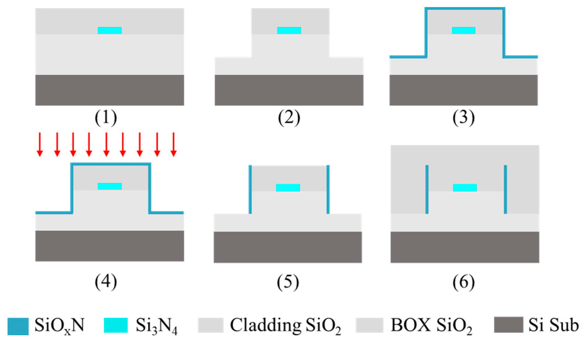
2.1. Development and Description of the Model

Our proposed edge coupling structure consists of three primary sections, as shown in Figure 1a–c. First, a double-layer SiOxN thin-film waveguide structure is designed for end-face coupling. It consists of two perpendicular SiOxN layers on a substrate, with an intermediate and cladding SiO2 layers forming the waveguide. The height of each SiOxN layer is denoted as H, and the gap between them as G. By precisely controlling these parameters, the mode size at the output can be effectively expanded, thereby enhancing mode matching with the fiber. Second, To ensure a smooth transition and minimize mode conversion losses, an adiabatic tapering section is employed. In this section, both the SiOxN and Si3N4 waveguides are gradually tapered. The gap G between the SiOxN layers and the central waveguide dimension gradually increase, enabling a seamless mode evolution from the double-layer SiOxN mode to the Si3N4 mode, as shown in Figure 1d. Lastly, a transition section connects the Si3N4 slab waveguide to a ridge waveguide using standard adiabatic taper. In the simulation model, the thickness of the silicon dioxide layer is fixed at 100 nm. The gap G2 between the SiOxN layers is set to 5 μm to ensure no coupling occurs between the Si3N4 waveguide and the SiOxN films. The simulated central wavelength is 1.55 µm, and the material dispersion is investigated. The refractive index values used in the modeling at the central wavelength of 1.55 µm are as follows: SiO2 has a refractive index of 1.44, Si3N4 has a refractive index of 2.0, and SiOxN has a refractive index of 1.7. We chose the silicon nitride strip waveguide with a total thickness of 400 nm as a study-case. The double-layer SiOxN thin-film waveguide structure can be fabricated with the self-aligned etching process [16]. The self-aligned etching process is a widely used technique in MOS transistor manufacturing, primarily for accurately defining and controlling the size and structure of specific regions [17,18,19].

2.2. Modeling Methods

The coupling efficiency of an edge coupler can be described as the product of two key factors: the overlap efficiency between the optical fiber mode and the mode at the coupler tip near the chip facet ( η 1 ), and the transformation efficiency from the delocalized mode at the facet to the mode of the nominal interconnecting waveguide ( η 2 ). η 1 refers to the coupling efficiency between the end face of the integrated photonic waveguide and the optical fiber. η 2 represents the efficiency of mode conversion from the waveguide to the end-face structure. The product of these two efficiencies ( η 1   ×   η 2 ) defines the overall efficiency of the end-face coupling structure.
For quasi-TE and quasi-TM polarizations, the coupling efficiency between the optical fiber and the chip edge facet can be obtained by calculating the overlap integral of the mode fields of the optical fiber and chip edge facet [20]. The definition of the mode overlap efficiency η 1   can be expressed as follows:
η 1 = | E 1 × E 2 d A | 2 E 1 2 d A × E 2 2 d A ,
where A is the modal distribution area, while E1 and E2 represent the electric fields of the fiber mode and the superimposed mode at the coupler facet, respectively. The mode transformation efficiency ( η 2 ) is determined by the design details of the taper structure, which facilitates the conversion of the mode at the chip facet into the mode of the interconnecting waveguide. Coupling loss is usually used to describe how much energy is lost during coupling, which can be transformed with coupling efficiency η as follows:
C o u p l i n g   L o s s = 10 × l o g 10 η .
The design process is carried out in two stages. Initially, the transverse field overlap between the optical fiber mode and the waveguide mode at the chip facet is optimized. In the second stage, a longitudinal taper structure is developed to convert the delocalized mode near the facet into the mode of the silicon nitride wire interconnecting waveguide.

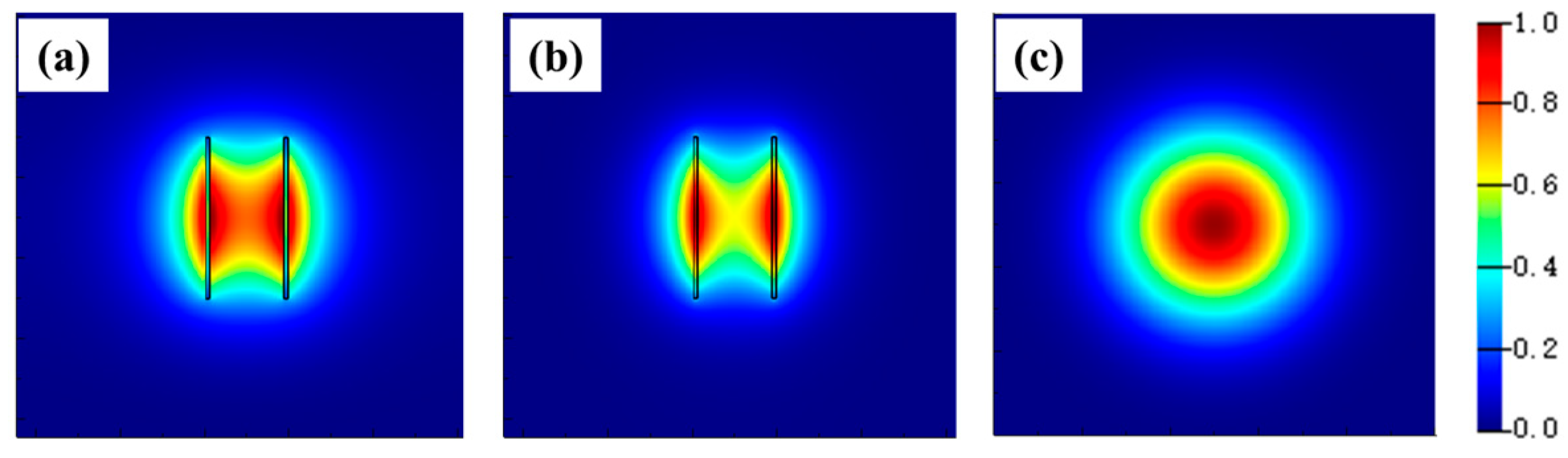
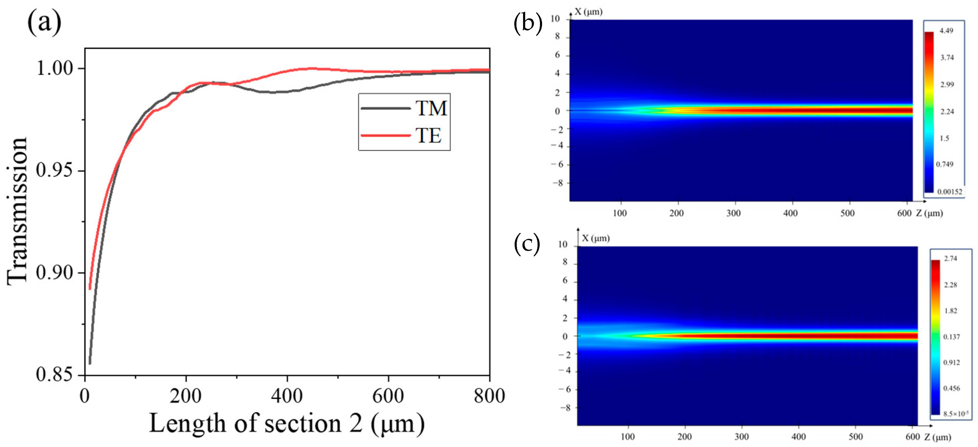
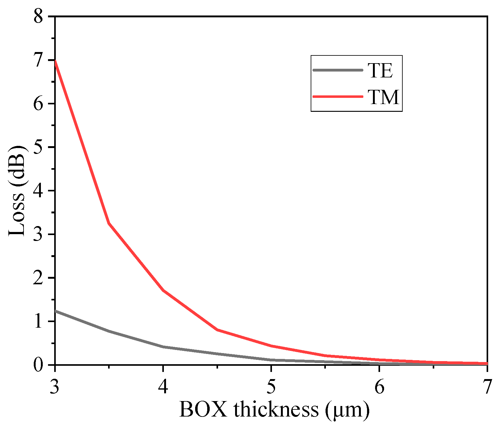
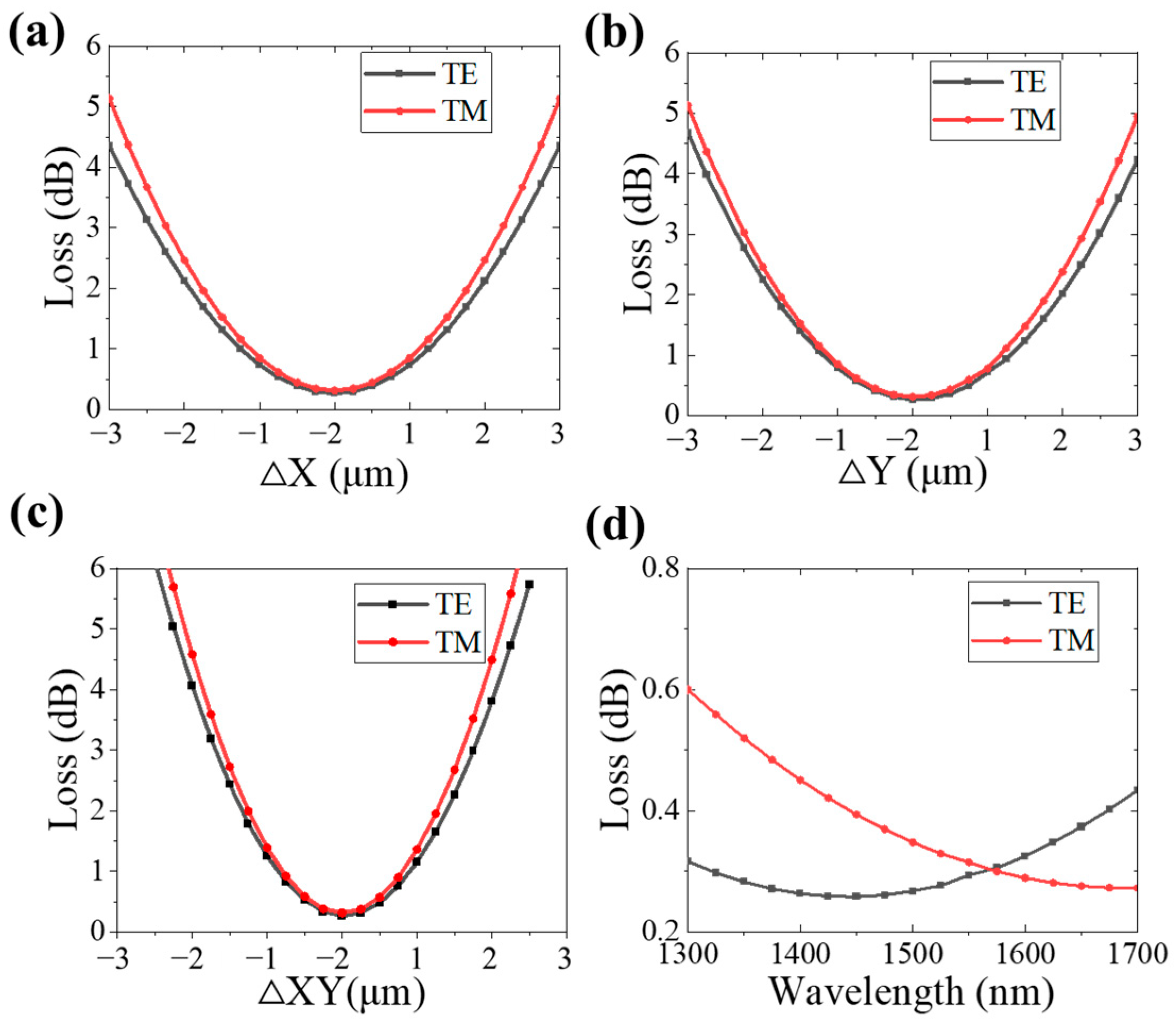
2.3. Modeling Results

In Figure 2, we present the simulation results of the coupling loss between the end-face coupler and fibers with different mode field diameters (MFDs) by systematically varying the Si3N4-height and SiOxN-gap of the end-face structure. The coupling loss for both TE and TM modes, as well as the polarization-dependent loss (PDL) [21], were calculated. The results indicate that the optimal SiOxN height and SiOxN gap for achieving the minimum coupling loss increase with increasing MFD. For instance, for a fiber with an MFD of 8 μm, the optimized structure is H = 4.5 μm and G = 2.5 μm, offering a coupling loss of TE = 0.4 dB and TM = 0.6 dB, while the PDL is 0.17 dB. For a fiber with MFD = 5 μm, the optimized structure is H = 3.5 μm and G = 1.0 μm, offering the coupling loss of TE = 0.56 dB and TM = 0.30 dB, while the PDL is 0.26 dB. We selected H = 4 μm and G = 1.75 μm as the optimal design for a fiber with an MFD of 6 μm, achieving the lowest coupling loss (TE = 0.29 dB, TM = 0.31 dB) and near-zero PDL (PDL = 0.02), and demonstrating a favorable balance between coupling loss and alignment tolerance. Figure 3 shows the mode field distribution of the selected end-face structure and the fiber with an MFD of 6 μm. The Gaussian-like mode field profile of the fiber matches that of the end-face structure, minimizing mode mismatch loss with a η 1 of 98%.
In the design outlined in Section 2, tapered structures are utilized to facilitate the transition from a 400 nm silicon nitride strip waveguide into a double-layer SiOxN waveguide. A key feature of the transformation structure is that a smaller tip dimension typically results in a higher conversion efficiency. In our simulation, the taper tip’s minimum feature size is strategically set to 100 nm to optimize manufacturability and performance. The Lumerical’s EigenMode Expansion (EME) method was utilized to calculate the transmission efficiencies of both transverse electric (TE) and transverse magnetic (TM) modes, relative to the length of Section 2, as depicted in Figure 4a. The results indicate that for lengths exceeding 600 microns, both TE and TM modes attain exceptionally high conversion efficiencies, consistently surpassing 99%. Sub-wavelength grating (SWG) structures [22] are integrated to decrease the transition length. However, such integrations also escalate manufacturing complexity and can lead to additional optical losses. Figure 4b,c provide further insight into smooth mode transition by illustrating the electric field evolution of the TE and TM modes, respectively, when the length of the transition length is set to 600 μm.
In edge coupler designs, substrate leakage loss is a critical consideration, especially as the optical mode size expands significantly in the Spot Size Converter (SSC) region. The optical field’s extension into the substrate can result in additional propagation losses, primarily influenced by the thickness of the BOX layer separating the silicon substrate from the waveguide. To investigate this effect, we performed simulations to calculate the substrate leakage loss in the region where the mode size is maximized. The simulation considered varying BOX layer thicknesses and evaluated the corresponding leakage loss for both TE and TM polarizations. A transmission length of 500 μm was chosen for the analysis to ensure the results reflect the leakage behavior over a sufficiently long propagation distance. The results are summarized in Figure 5. It can be seen that for BOX thicknesses of 6 μm or greater, the leakage loss for both TE and TM polarizations falls below 0.1 dB, effectively eliminating substrate leakage as a significant source of loss.
Finally, the alignment tolerance of the end-face coupling structure with the fiber was analyzed in detail, including both the horizontal (△X) and vertical (△Y) directions. Figure 6a,b present the coupling loss of the TE and TM modes under different alignment tolerances, respectively. The results demonstrate a remarkably large alignment tolerance of the proposed structure. Both the TE and TM modes can achieve a ±2.5 μm alignment tolerance with a 3 dB penalty in both the X and Y directions. It should be noted that while an optimized design with larger H and G can further improve alignment tolerance, it inevitably leads to higher coupling loss and PDL. Furthermore, we have expanded our tolerance analysis to account for the simultaneous variation in both the X and Y directions, as shown in Figure 6c. For the simultaneous variation in both the X and Y directions, the 3 dB alignment tolerance was reduced to ±1.75 μm. This reflects the more stringent tolerance requirements when both axes are varied together and demonstrates the effect of correlated variations in fabrication. The impact of wavelength on coupling loss was investigated, as shown in Figure 6d. Simulation results over the ultra-broadband wavelength range of 1300–1700 nm show that the coupling loss of the TE mode is less than 0.45 dB, with a variation of less than 0.2 dB, while the coupling loss of the TM mode is less than 0.6 dB, with a variation of less than 0.3 dB. These results indicate that the proposed end-face coupling structure exhibits excellent performance in terms of alignment tolerance and wavelength independence.

3. Discussion

In this paper, we have proposed a novel end-face coupling structure that offers excellent properties. To obtain a better assessment, we summarize the comparison between our device and several designs in Table 1. As shown, our proposed device demonstrates excellent coupling efficiency for both TE and TM modes, leading to ultra-low polarization-dependent loss (PDL). At the same time, it maintains a large mode size, which is well-matched to fibers with an MFD of 6 μm. This large mode size significantly enhances alignment tolerance, further improving the practicality of our device.
In the development of our photonic structures, we have implemented a vertically aligned SiOxN thin-film layer on the substrate, distinguishing our structure from the conventional horizontal film structures typically employed in end-face coupler designs. Vertically aligned SiOxN thin-film layers can be fabricated with a self-aligned technique commonly used in the production of MOS transistors in integrated circuits [16,17,18,19]. This method allows for the precise placement and alignment of the SiOxN film layers relative to the underlying silicon nitride waveguides. The core concept involves depositing a thin film directly onto the etched substrate, followed by reactive ion etching (RIE) without the need for an additional photolithography step. Due to the anisotropic nature of RIE, the etching is much more effective in the vertical direction, allowing complete removal of the film from horizontal surfaces while preserving the film on the vertical sidewalls.
The fabrication process of the proposed structure involves several key steps, as shown in Figure 7. First, the end-face silicon nitride waveguide begins with the etching of the strip waveguide structure, followed by deposition of a 3 μm thick silicon oxide cladding layer. Next, a silicon oxide layer is patterned and etched using a dry etching process with vertical sidewalls. A metal hard mask is typically used in this step to achieve a high aspect ratio. After etching the silicon dioxide, a 100 nm thick SiOxN thin film is deposited over the structured silicon dioxide layer using low-pressure chemical vapor deposition. Following deposition, the SiOxN layer undergoes a selective etching process using reactive ion etching without the need for photolithographic patterning. Finally, larger than 3 um cladding oxide is deposited using either PECVD or LPCVD. This self-aligned approach to layer deposition and patterning simplifies the fabrication process while enhancing the precise thickness control of the SiOxN layers, ensuring robust control over the optical path and interactions within the device.

4. Conclusions

In summary, we have proposed a novel end-face coupling structure that offers exceptional performance in terms of coupling loss, alignment tolerance, and polarization independence. By carefully engineering the double-layer SiOxN thin-film waveguide, we have achieved a highly optimized design that minimizes coupling loss while maintaining a large tolerance for alignment errors. Specifically, the proposed structure exhibits a coupling loss of 0.29 dB for the TE mode and 0.31 dB for the TM mode, along with a large 3 dB alignment tolerance of ±2.5 μm in both the horizontal and vertical directions and a polarization-dependent loss (PDL) of 0.02 dB. Our proposed method provides a new way of realizing a high-performance edge coupler for a wide range of photonic applications.
We believe our work paves the way for high-performance coupling solutions for silicon nitride (Si3N4) photonic integrated circuits.

Author Contributions

Conceptualization, Z.C. and L.Z.; Data curation, Z.C. and Z.H.; Formal analysis, Z.C., X.F. and Z.H.; Funding acquisition, Z.H.; Investigation, Z.C.; Methodology, Z.C.; Project administration, Z.H.; Software, Z.C. and X.F.; Supervision, Z.H.; Validation, Z.C. and Z.H.; Writing—original draft, Z.C.; Writing—review and editing, Z.C. All authors have read and agreed to the published version of the manuscript.

Funding

This research was funded by the National Key Research and Development Plan (2022YFB2802401), the National Key Research and Development Program (2021YFB2401600), and the Strategic Priority Research Program of Chinese Academy of Sciences (XDB43000000).

Institutional Review Board Statement

Not applicable.

Informed Consent Statement

Not applicable.

Data Availability Statement

The data presented in this study are available from the corresponding authors upon reasonable request.

Conflicts of Interest

The authors declare no conflicts of interest.

References

  1. Xiang, C.; Jin, W.; Bowers, J.E. Silicon nitride passive and active photonic integrated circuits: Trends and prospects. Photonics Res. 2022, 10, A82–A96. [Google Scholar] [CrossRef]
  2. Bauters, J.F.; Heck, M.J.; John, D.; Tien, M.C.; Li, G.; Barton, J.S.; Leinse, A.; Heideman, R.G.; Blumenthal, D.J.; Bowers, J.E. Silicon on ultra-low-loss waveguide photonic integration platform. Opt. Express 2013, 21, 544–555. [Google Scholar] [CrossRef] [PubMed]
  3. Marchetti, R.; Lacava, C.; Bianchi, G.M.; Ramirez, J.M.; Vezzoni, M.; Fontana, G.; Minkov, A.; Frigerio, J.; Carbone, L.; Galli, M.; et al. Coupling strategies for silicon photonics integrated chips. Photonics Res. 2019, 7, 201–239. [Google Scholar] [CrossRef]
  4. Mu, X.; Zhuang, L.; Fan, Y.; Hoekman, M.; Leinse, A.; Roeloffzen, C.G. Edge couplers in silicon photonic integrated circuits: A review. Appl. Sci. 2020, 10, 1538. [Google Scholar] [CrossRef]
  5. Bhandari, B.; Shrestha, S.; Khanna, R.; McKinney, J.R.; Zhou, W. Compact and broadband edge coupler based on multi-stage silicon nitride tapers. IEEE Photon. J. 2020, 12, 1–11. [Google Scholar] [CrossRef]
  6. Suchoski, P.; Ramaswamy, R. Design of single-mode step-tapered waveguide sections. IEEE J. Quantum Electron. 1987, 23, 205–211. [Google Scholar] [CrossRef]
  7. Dewanjee, A.; Rahman, A.B.M.; Poletti, F.; Rahman, M.S.; Sessions, N.P. Demonstration of a compact bilayer inverse taper coupler for Si-photonics with enhanced polarization insensitivity. Opt. Express 2016, 24, 28194–28203. [Google Scholar] [CrossRef]
  8. Kruse, K.; Middlebrook, C.T. Polymer taper bridge for silicon waveguide to single mode waveguide coupling. Opt. Commun. 2016, 362, 87–95. [Google Scholar] [CrossRef]
  9. Doylend, J.K.; Knights, A.P. Design and simulation of an integrated fiber-to-chip coupler for silicon-on-insulator waveguides. IEEE J. Sel. Top. Quantum Electron. 2006, 12, 1363–1370. [Google Scholar] [CrossRef]
  10. Voigt, K.; Brulis, V.; Petermann, K.; Zimmermann, L. Study of backend waveguide arrays for adiabatic coupling to Si waveguides. In Proceedings of the 2017 IEEE 14th International Conference on Group IV Photonics (GFP), Berlin, Germany, 23–25 August 2017; pp. 143–144. [Google Scholar]
  11. Holly, R.; Tönshoff, P.; Völkel, R.; Herzig, H.P. Fabrication of silicon 3D taper structures for optical fibre to chip interface. Microelectron. Eng. 2007, 84, 1248–1251. [Google Scholar] [CrossRef]
  12. Shiraishi, K.; Takahashi, S.; Ishikawa, Y.; Yamashita, K. A silicon-based spot-size converter between single-mode fibers and Si-wire waveguides using cascaded tapers. Appl. Phys. Lett. 2007, 91, 141112. [Google Scholar] [CrossRef]
  13. Fang, Q.; Song, J.; Ding, J.F.; Lo, G.Q.; Kwong, D.L. Suspended optical fiber-to-waveguide mode size converter for silicon photonics. Opt. Express 2010, 18, 7763–7769. [Google Scholar] [CrossRef]
  14. Chen, L.; Doerr, C.R.; Chen, Y.-K.; Liow, T.Y. Low-loss and broadband cantilever couplers between standard cleaved fibers and high-index-contrast Si3N4 or Si waveguides. IEEE Photon. Technol. Lett. 2010, 22, 1744–1746. [Google Scholar] [CrossRef]
  15. Fang, Q.; Song, J.; Wu, H.; Lo, G.-Q.; Kwong, D.-L. Mode-size converter with high coupling efficiency and broad bandwidth. Opt. Express 2011, 19, 21588–21594. [Google Scholar] [CrossRef] [PubMed]
  16. Shiu, W.; Vacar, J.; Yu, H.; Choi, T.; Rossel, C. Advanced self-aligned double patterning development for sub-30-nm DRAM manufacturing. Opt. Microlithogr. XXII SPIE 2009, 7274, 72743U. [Google Scholar]
  17. Chen, R.; Li, Y.C.; Cai, J.M.; Cao, K.; Lee, H.B.R. Atomic level deposition to extend Moore’s law and beyond. Int. J. Extrem. Manuf. 2020, 2, 022002. [Google Scholar] [CrossRef]
  18. Rim, K. Strained Si CMOS (SS CMOS) technology: Opportunities and challenges. Solid-State Electron. 2003, 47, 1133–1139. [Google Scholar] [CrossRef]
  19. Schroder, D.K. Semiconductor Material and Device Characterization, 3rd ed.; John Wiley & Sons: Hoboken, NJ, USA, 2006. [Google Scholar]
  20. Papes, M.; Hsieh, M.; Chrostowski, L.; Shekhar, S. Fiber-chip edge coupler with large mode size for silicon photonic wire waveguides. Opt. Express 2016, 24, 5026–5038. [Google Scholar] [CrossRef]
  21. Xu, L.H.; Shi, Y. Ultra-compact polarization-independent directional couplers utilizing a subwavelength structure. Opt. Lett. 2017, 42, 5202–5205. [Google Scholar] [CrossRef] [PubMed]
  22. Halir, R.; Bock, P.J.; Cheben, P.; Ortega-Moñux, A.; Alonso-Ramos, C.; Schmid, J.H.; Lapointe, J.; Xu, D.-X.; Wangüemert-Pérez, J.G.; Molina-Fernández, I.; et al. Waveguide sub-wavelength structures: A review of principles and applications. Laser Photonics Rev. 2015, 9, 25–49. [Google Scholar] [CrossRef]
  23. Zhu, X.; Li, G.; Wang, X.; Li, Y.; Davidson, R.; Little, B.E.; Chu, S.T. Low-loss fiber-to-chip edge coupler for silicon nitride integrated circuits. Opt. Express 2023, 31, 10525–10532. [Google Scholar] [CrossRef] [PubMed]
  24. Zhang, Y.; Liu, Y.; Cao, X.; Wang, L.; Mu, C.; Li, M.; Zhu, N.; Chen, W. High-Efficiency and Compact Polarization-Insensitive Multi-Segment Linear Silicon Nitride Edge Coupler. Photonics 2023, 10, 510. [Google Scholar] [CrossRef]
  25. Mu, X.; Wu, S.; Cheng, L.; Tu, X.; Fu, H.Y. A Compact Adiabatic Silicon Photonic Edge Coupler Based on Silicon Nitride/Silicon Trident Structure. In Proceedings of the 2019 18th International Conference on Optical Communications and Networks (ICOCN), Huangshan, China, 5–8 August 2019; pp. 1–3. [Google Scholar]
  26. Sun, S.; Chen, Y.; Sun, Y.; Liu, F.; Cao, L. Novel Low-Loss Fiber-Chip Edge Coupler for Coupling Standard Single Mode Fibers to Silicon Photonic Wire Waveguides. Photonics 2021, 8, 79. [Google Scholar] [CrossRef]
Figure 1. Schematic of the end-face coupling structure. (a) 3D view of the end-face coupling structure. (b) Top view of the structure. (c) Cross-sectional view of the structure. (d) Mode evolution diagram.
Photonics 12 00136 g001
Figure 2. Impact of different SiOxN heights (H) and gaps (G) on coupling loss between double-layer SiOxN film edge coupler and fibers with different MFDs: (a) TE mode coupling loss, (b) TM mode coupling loss, (c) PDL.
Photonics 12 00136 g002
Figure 3. Mode profile comparison between the optimized structure (H = 4 μm, G = 1.75 μm) of Section 1 and fiber: (a) TE Mode and (b) TM Mode of Section 1; (c) Fiber Mode (MFD = 6 μm).
Photonics 12 00136 g003
Figure 4. Simulation results for (a) transmission efficiencies of TE and TM modes versus the taper length of Section 2 (G1 = 1.75 μm, G2 = 5 μm, W_tip = 100 nm, W = 1 μm). Electric field evolution of Section 2 for (b) TE mode and (c) TM mode at 600 μm section length.
Photonics 12 00136 g004
Figure 5. Simulated substrate leakage loss of 500 μm propagation length as a function of BOX thickness.
Photonics 12 00136 g005
Figure 6. Alignment tolerance analysis of the end-face coupling structure: (a) horizontal (△X), (b) vertical (△Y) directions, (c) simultaneous variation in horizontal and vertical (△XY), and (d) wavelength dependence of coupling loss.
Photonics 12 00136 g006
Figure 7. Fabrication process of the proposed structure: (1) silicon nitride waveguide pattern and cladding silicon oxide deposition, (2) silicon oxide pattern, (3) SiOxN deposition, (4) Anisotropic RIE etching process (red arrows), (5) after RIE etching process, (6) final cladding silicon oxide deposition.
Photonics 12 00136 g007
Table 1. Comparison of various edge couplers.
Device StructureCoupling Loss TE/TMPDLMFD3dB ToleranceWaveguide TypeExperiment
Inverse taper [5]0.36/0.56 dB0.2 dB4 μm±1.75 μm500 nm Si3N4Yes
Multiple-taper design [7]1.5/2 dB1 dB5 μmNot shown220 nm SiliconYes
Silica glass waveguide [23]0.6/0.8 dB0.2 dB10.4 μm±4.5 μm750 nm Si3N4Yes
Multi-Segment Inverse-taper [24]0.22/0.31 dB0.09 dB3.2 um±1.4 μm400 nm Si3N4No
Trident layers [25]0.91 dB (TE)/3.2 umNot shown400 nm Si3N4No
Multiple layer structure [26]0.62/0.44 dB0.25 dB8.2 μmNot shown220 nm SiliconNo
This work0.29/0.310.02 dB6 μm±2.5 μm400 nm Si3N4No
Disclaimer/Publisher’s Note: The statements, opinions and data contained in all publications are solely those of the individual author(s) and contributor(s) and not of MDPI and/or the editor(s). MDPI and/or the editor(s) disclaim responsibility for any injury to people or property resulting from any ideas, methods, instructions or products referred to in the content.

