1. Introduction
Lithium niobate (LiNbO3, LN) is widely used in photonic devices and integrated optical systems because of its excellent electro-optic, thermo-optic, and nonlinear effects and wide transparent window [
1,
2,
3]. With breakthroughs in nanofabrication technology, the successful manufacturing of lithium niobate on insulator (LNOI) makes it possible to integrate high-performance nanophotonic systems [
4,
5,
6]. With the rapid development seen in recent years, some devices based on LNOIs have been widely developed, such as electro-optical modulators [
7,
8,
9,
10,
11,
12], optical frequency combs [
13,
14,
15,
16], and wavelength converters [
17]. A power splitter is an essential component for integrated functional photonic systems. With the large-scale integration of various devices and functions on a single thin-film lithium niobate chip, the complexity of the functions leads to the need for arbitrarily proportional power dividers for signal monitoring. Furthermore, an arbitrary-ration 1 × 2 power splitter could lead to large-scale ultra-low loss photonic circuits for various quantum and classical applications, including feed-forward photonic quantum computation.
Common structures that can realize arbitrary splitting ratios include directional couplers (DCs), 1 × 2 MZIs, and asymmetric Y-branches. However, they are typically limited by size, wavelength sensitivity, and manufacturing tolerances, significantly limiting their application. Multimode interference (MMI) couplers can effectively solve the above problems. MMI couplers are essential in modern photonics and optoelectronic integrated circuits because of their low loss, large process tolerance, and large bandwidth. Integrated optical power splitters are very attractive. Conventional 1 × 2 MMI can only realize an equal proportion of light splitting [
18]. However, changing the multimode area’s shape makes it possible to achieve arbitrary proportional beam splitting [
19,
20,
21]. Although people have already studied the properties of different asymmetrical multimode interference structures (A-MMIs) based on the SOI [
18], it is still necessary to study the thin-film lithium niobate material due to its uniqueness.
Therefore, in this paper, we demonstrate the compact and low-loss A-MMIs of any spectral ratio based on 600 nm thick thin lithium niobate films. The performance of the A-MMIs on an LNOI was simulated and characterized. Theoretically, the structure can realize arbitrary proportions of spectral ratios. As a proof of concept, one conventional MMI structure and five A-MMI structures with different spectral ratios were designed and fabricated in this study. A single device’s distribution ratio and insertion loss were obtained by linear fitting through the design of the cascade structure. The simulation and experiment show that the insertion loss of the device rises with the increase in the distribution ratio. According to the test results, the device’s insertion loss at a wavelength of 1550 nm increases from 0.1 dB to 0.9 dB.
2. Device Design and Fabrication
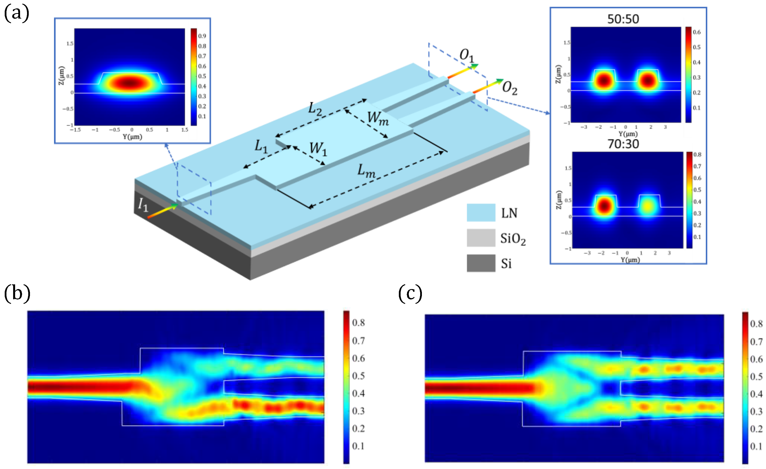
The proposed A-MMI power splitter based on an LNOI is shown in
Figure 1a. This device is designed on an X-cut LNOI with a 600 nm thick LN thin film, a 2 μm SiO
2 insulation layer, and a 525 μm thick high-resistance silicon substrate. The waveguides are ridge-type with a rib height of 300 nm and a slab thickness of 300 nm. The upper cladding is SiO
2 with a thickness of 800 nm to protect the device. The signal light is injected into the multimode region through a 1.5 μm wide waveguide and then tapered to reach a width of 2 μm. The two tapered output waveguides are precisely positioned at the first two folded images at ±
We/6 [
15].
Where the “effective” width
We considers the polarization-dependent lateral penetration depth of each mode field, associated with the Goos–Hähnchen shifts at the ridge boundaries.
where
nr denotes the ridge effective refractive index,
λ0 is the operating wavelength,
nc denotes the cladding effective refractive index,
Wm is the width of the multimode waveguide, and
σ = 0 for TE and
σ = 1 for TM. Here, we will only consider the TE model for the time being.
The tapers of the A-MMI are engineered to maximize the incoming and outgoing light from the multimode region, all with the same structure. The input and output lights are shown in
Figure 1a. The proposed device features an asymmetric multimode interference region. Compared to the conventional MMI, the only difference is that the symmetry of the multimode region is broken by removing its top left corner. This small structural change causes a dramatic redistribution of the optical mode field (
Figure 1b,c). When the output waveguide is also located in the first double image position, the power output from the lower port will be greater than that from the upper port, as shown in
Figure 1b. Here, we denote
O1 and
O2 as the optical power output from the upper and lower ports, respectively, and the power splitting ratio (
PSR) is given by:
The traditional MMI was first designed and simulated based on the 3D finite-difference time–domain (FDTD) solver to meet the compactness requirements and search for the position of the double image. The working principle of the MMI coupler is based on the so-called self-imaging theory: in a multimode waveguide, the input field can be reproduced in single or multiple images at periodic intervals along the direction of field propagation [
15]. For 1 × 2 MMI couplers, a double image is required. In order to achieve isometric splitting and minimum insertion loss of the device, the multimode region (
Wm ×
Lm) is 5.8 μm × 26.4 μm by parameter scanning, and the optimal splitting ratio performance can be achieved when the position of the two output optical ports is 1.56 μm away from the center. Based on the traditional MMI simulation optimization, the structure of the multimode region is optimized. Due to the weak distribution of the light field in the corners, removing a certain area brings less additional loss. However, the value of
W1 needs to be reasonably designed because the size of the multimode region will be too small when
W1 is too large, and it is not easy to realize an arbitrary beam-splitting ratio when
W1 is too small. The insertion loss of the device is minimized when
W1 = 3.9 μm, and unequal light can be achieved by changing the length of
L1.
The relations between the PSR and the removed rectangle length (
L1) are shown in
Figure 2a, where the measured and simulated results agree quite well. With a constant width of
W1, as the length of
L1 increases, the PSR increases accordingly. The corresponding multimode region length (
Lm) is plotted in
Figure 2b, where the blue dots show the actual dimensions at the time of fabrication. The PSR varies from 50:50 to 100:0 while
L1 increases. At the same time, the first two-fold image shifts slightly toward a farther position, that is, the length of the multimode region increases, as shown in the insets of
Figure 2b. In all cases, the dimension of the multimode region is in the range of 5.8 μm × (26.4–35.6) μm, which is very compact for large-scale integration. Overall, by changing the values of
L1 and
Lm, we can obtain arbitrary-ratio 1 × 2 power splitters.
Here, the devices with PSRs of 50:50, 60:40, 70:30, 80:20, 90:10, and 95:5 are experimentally demonstrated, and their corresponding values of
L1 and
Lm and simulated insertion loss are listed in
Table 1. It is worth noting that the device dimensions presented in this work are specifically designed for the TE
0 mode due to the difference in the “effective” width
We of the TE and TM modes. However, later on, we also showed that this structure is suitable for TM
0 mode.
To evaluate the validity of our hypotheses and simulations, we designed six devices with different spectral ratios: 50:50, 60:40, 70:30, 80:20, 90:10, and 95:5. The devices were fabricated using a commercially available X-cut LN-on-insulator (LNOI) substrate with 600 nm thick LN thin film bonded on top of 2 μm thick silica. A 200 nm thick chromium layer acting as a hard-etching mask is first deposited on top of the LNOI using electron beam evaporation. Electron-beam lithography (EBL) is used to draw waveguide patterns on hydrogen silsesquioxane (HSQ) resist. These patterns are set so that the direction of light propagation is along the Y-axis of the crystal. Then, the designs are transferred into the chromium layer using normal ICP-RIE etching (ICP-RIE) and subsequently into the LN thin-film via an optimized etching recipe in ICP-RIE using an Ar-based gas mixture. The etch rate is around 30 nm/min, and the depth of the LN etch is 300 nm. The sidewall angle of the waveguide is greater than 75°. Finally, an 800 nm thick silica cladding layer is then deposited on top of the waveguides using PECVD.
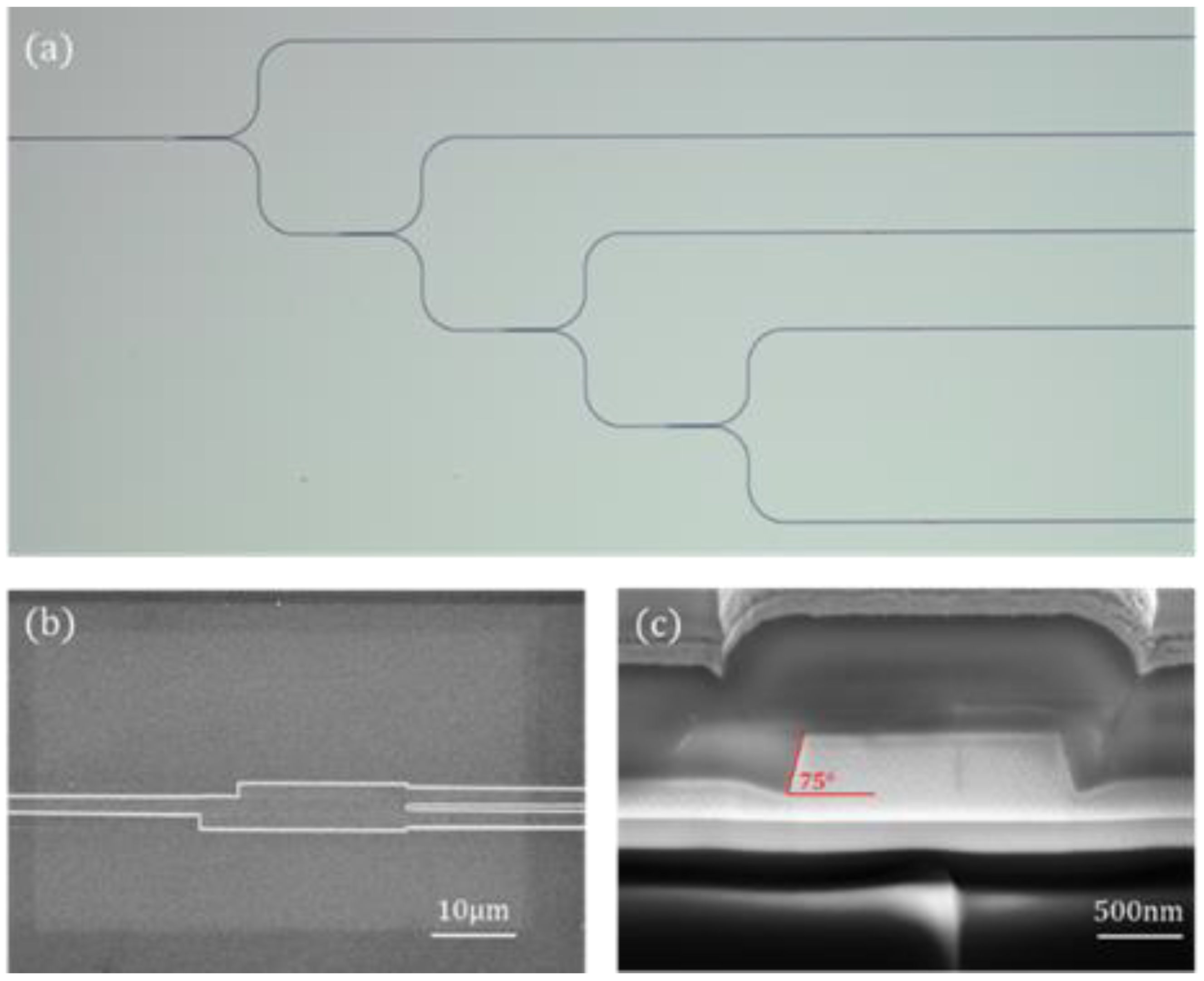
Figure 3a shows the microscope image of the fabricated device and an SEM image of a single A-MMI and the cross-section of the LN waveguide.
3. Results and Discussion
To test the devices, we placed the chip on a six-axis nano-positioning stage (Apico) and used a tunable laser (SANTEC TSL-570) as a light source coupled through a lensed fiber to the input port of the chip. At the output port, we used a photodetector (AP-OPM-02-HAS-Q-AQ) to observe the device output power in real time. We cascaded multiple devices in series to obtain precise and reliable measurements of the devices’ PSR and insertion loss. The devices were arranged for characterization in a cascade configuration where each “weak output” is measured and the “strong output” is connected to a subsequent A-MMI. By comparing the transmission of different branches, the excess loss and PSR of the device can be derived.
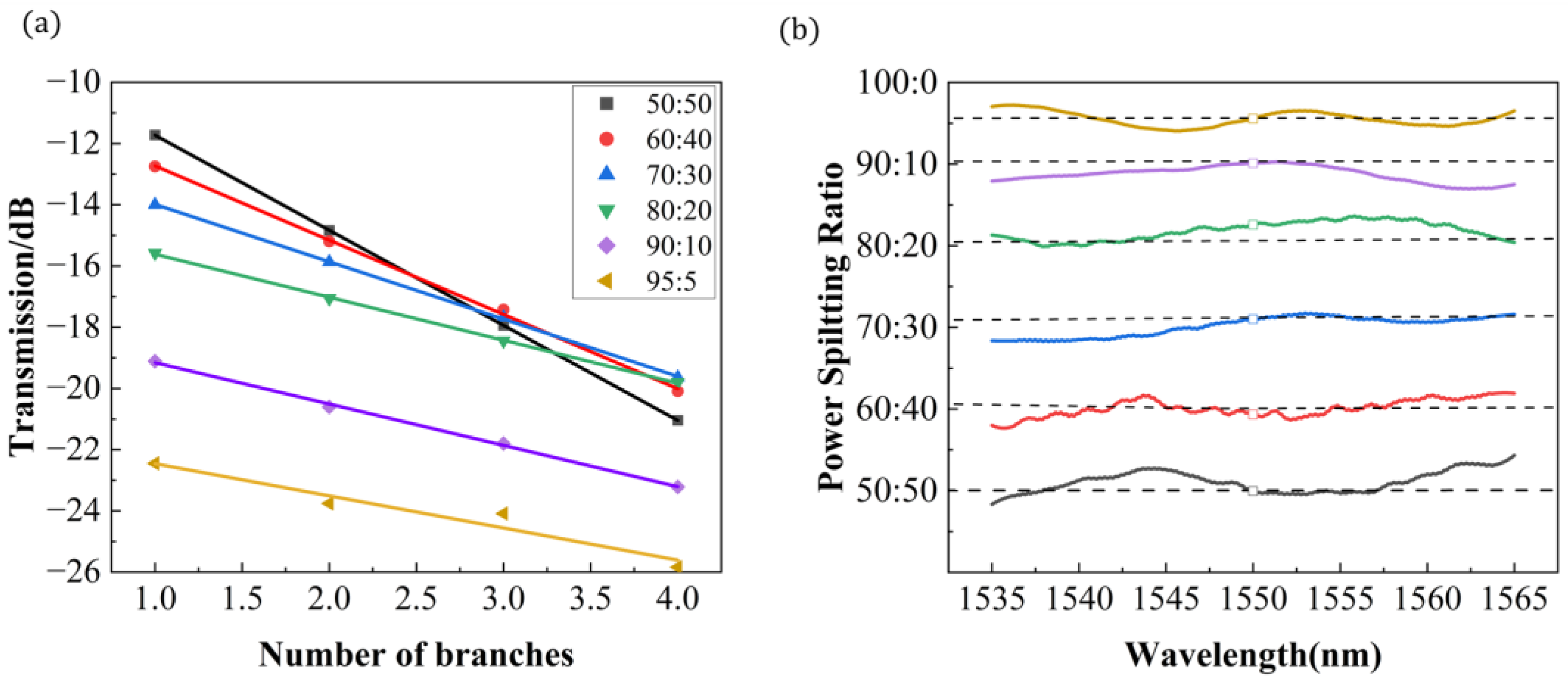
Figure 4a shows the measurement results of TE mode at a 1550 nm wavelength. The data are fitted linearly, and the equation of the fitted line is given. The slope (
k) and intercept (
b) are shown in
Table 2. The insertion loss (
IL) can be extracted from the difference between the slope of the fitted line (
k) and the actual distribution ratio (
a), and the relationship between
a and
IL is given by:
Since the lithium niobate material has a wide transparency window (350 nm to 5 μm), the intrinsic absorption loss is <0.001 dB/cm [
22], and the size of the devices we designed is small; the material absorption loss has little effect on the device loss. The intercept (
b) represents the total coupling loss from the two fibers to the chip, and considering the curve trend, the interfacial loss (
f) for different splitting ratios can be expressed by the following equation:
Since the mode field size of the LNOI waveguide is much smaller than that of a single-mode fiber, in order to simplify the end-face coupling structure, a high numerical aperture UHNA7 fiber with a mode field diameter of about 3.2 μm was used. Therefore, the waveguide end faces are all forward wedge spot size converters (SSC) with end-face waveguide widths of 3 μm. Considering the process error of the end-face polishing and the coupling error, the average value of the device’s interfacial loss is therefore −8.4 dB, which is in good agreement with the current coupling efficiency of the 3 μm reverse wedge SSC.
The measured insertion losses of the A-MMI, as illustrated in
Table 2, are in the range of ~0.09–0.90 dB; this value is slightly higher than that of the simulated
IL (~0.06–0.73 dB). We think that the increased losses may be due to the device’s roughness, which is caused by the cavity symmetry being disrupted or a small deviation in the fabrication process. This could cause a systematic error.
In addition, the birefringence effect of the lithium niobate material due to the breaking of the symmetry of the cavity also leads to an intensification of the radiation loss of the device with the increase in the splitting ratio, which is manifested in the increase in the simulated insertion loss of the device. Therefore, the experimentally obtained insertion loss is mainly the scattering loss and radiation loss of the device. Further optimization of the fabrication process is expected to bring these values closer to the theoretical values.
Further experimental results regarding the wavelength dependence of the PSR are shown in
Figure 4. The instability of the PSR is due to measurement-induced effects, such as vibration in the coupling stage. In the wavelength range of 30 nm (1535–1565 nm), the variation in the PSR from both simulations (dashed lines) and measurements (solid lines) is less than 5%. Based on these measurements, we can conclude that the wavelength dependence of the proposed arbitrary ratio MMI power divider is weak.
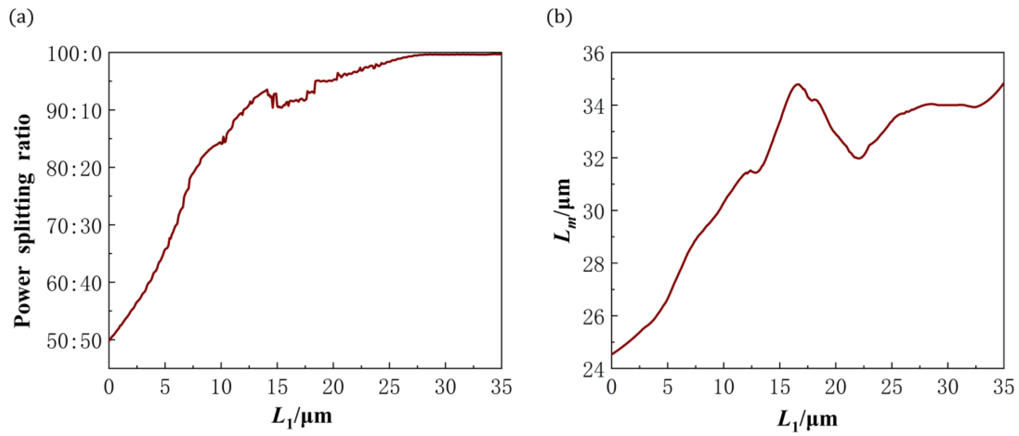
Finally, considering the birefringence effect of the lithium niobate material, we simulated the Z-cut-based A-MMI. Since r
33 maximizes its effect only when the light is vertically polarized, the TM mode is ideal in Z-cut LN-based devices. From Equation (1), for the TM mode,
We will change and therefore the position of the output waveguide will change. At this point, the two output optical ports are positioned 1.61 μm from the center. As shown in
Figure 5, this structure is still applicable for the TM mode. When
L1 = 15 m, a beam-splitting ratio of 95:5 can already be achieved, and the power redistribution is sufficiently drastic. However, as
L1 increases, the lengths of
L1 and
L2 are comparable, at which point the first dichroic image point will no longer move farther away, as evidenced by a decrease in
Lm, with the curve changing significantly after 15 μm. The strong performance of the A-MMIs in this manuscript can be used for functional devices and on-chip integrated circuits on the Z-cut TFLN platform.
4. Conclusions
In conclusion, we realized 1 × 2 A-MMI structures with an arbitrary splitting ratio based on the LNOI platform. The PSR can be well controlled by adjusting the shape of the multimode interference region. The devices are very small in size, and in all cases, the size of the multimode region is in the range of 5.8 μm × (26.4–35.6) μm, minimizing the impact on the overall footprint of the large-scale integrated LNOI chip. The simulation and experimental results show that the IL of the device increases with the increasing PSR, with it ranging from 0.1 dB to 0.9 dB at 1550 nm, and the PSR varies by less than 5% in the range of 1535–1565 nm. Further numerical analysis results show that the device structure is well-suited for TM mode. Our arbitrary-ratio 1 × 2 power splitters exhibit promising characteristics, making them potentially suitable for the on-chip power monitoring of large-scale LNOI-integrated functional photonic systems.
It is worth noting that a similar study to ours was published just recently [
23], in which the authors realized a one-in-two optical power divider with arbitrary splitting ratios based on 360 nm thick thin-film lithium niobate. Their multimode area size was maintained at 9.6 μm × (57.5–108) μm to achieve six different splitting ratios from 50:50 to 5:95, all with insertion losses below 0.3 dB. Compared to the above work, our devices are smaller; in all cases, the size of the multimode region is in the range of 5.8 μm × (26.4–35.6) μm. In addition, we used a cascade arrangement and derived the insertion loss of individual devices more accurately through linear fitting and then differencing. The test results are in good agreement with the simulations. Further simulations demonstrate that the structure is also suitable for use in TM mode on Z-cut LNOIs. This small-size, low-loss structure has a promising future in the design of complex photonic integrated circuits.


