1. Introduction
Photonic integrated circuits (PICs) possess significant potential in communication systems, sensing, biophotonics, and other fields [
1]. Over the years, substantial advancements have been made in diverse material platforms such as silicon (Si) [
2,
3], polymer [
4], indium phosphide [
5], lithium niobate (LN) [
6], and plasmonic materials [
7,
8,
9]. Among these, LN stands out as a favorable material for achieving high-performance optical modulators, primarily due to its exceptional electro-optic (EO) modulation properties stemming from the linear Pockels effect [
10]. Conventional LN modulators are typically created using low-index-contrast titanium-indiffusion or proton-exchange waveguides, offering limited optical confinement and approaching their physical limitations. However, the landscape of LN-based modulators has recently undergone a significant shift with the emergence of the LNOI platform [
11]. This platform has gathered considerable attention owing to its excellent material properties, including high index contrast, wide optical transparency (0.4–5 μm), and an exceptional linear electro-optic coefficient (r
33 = 31 pm/V) [
10,
12,
13,
14]. LNOI is viewed as a promising platform for high-performance optical modulators due to its potential for low insertion loss, a large electronic-optical bandwidth, and a low half-wave voltage.
Nevertheless, practical applications of LNOI modulators face a considerable challenge: significant optical losses resulting from mode mismatch and refractive index differences between optical fibers and LNOI optical waveguides [
10]. To address this issue, two primary solutions have been proposed: grating couplers and edge couplers [
15]. The grating coupler represents a periodic structure facilitating light coupling from the fiber into the waveguide through diffraction action at specific angles and polarizations [
16,
17]. Although grating couplers offer substantial alignment tolerances [
18,
19] and enable wafer-scale testing, they are constrained by low bandwidth, high insertion loss [
20,
21], polarization-dependence, and a complex fabrication process. In contrast, edge couplers rely on inverse tapers [
22,
23,
24]. By narrowing the tip’s width, they reduce light confinement, thereby broadening the spatial distribution of the mode profile and minimizing mode mismatch between the fiber and the waveguide. Additionally, the waveguide’s effective index gradually decreases as more mode fields leak into the cladding, resulting in low absorption loss. Compared to grating couplers, edge couplers boast advantages such as a wider optical bandwidth, polarization independence, and reduced coupling loss.
Various edge coupler designs have been proposed on multiple material platforms. On the Si platform, a 3D waveguide structure has been introduced with continuous tapered variations in width and height [
25]. This structure utilizes the space of the buried oxide (BOX) on a standard silicon-on-insulator wafer, resulting in a planar top wafer surface. This design allows for further processing of the chip without any restrictions. The proposed structure enables coupling with standard single-mode 220 nm thick silicon waveguides and large-core waveguides measuring approximately 3 μm in width, 1.5 μm in height, and a BOX thickness of 2 μm, achieving a coupling loss of 0.56 dB. In [
26], two 3D-structured edge couplers were proposed and manufactured on the Si platform, comprising forward adiabatic taper and semi-cone structures. The coupling losses for these two structures in the TE mode were reported as 0.97 and 0.78 dB, respectively. Silicon nitride (SiN) has emerged as a promising material for PICs due to its low loss, broadband transparency, and compatibility. The use of SiN as the interface for edge couplers has garnered significant attention. In [
27], a high aspect ratio inverse tapered waveguide based on the silicon nitride platform was designed. With an inverse tapered structure having minimum/maximum tips at 800 nm and 2.8 μm, respectively, the design achieved losses less than 0.2 dB/facet across the entire C-band when interfacing with a stand SMF. Also, a variety of edge coupler configurations on the LNOI platform have been recently documented. One such configuration utilized an edge coupler featuring an LN bilayer inversely tapered mode converter, achieving an insertion loss of 1.7 dB/facet when coupled with a lensed SMF with an MFD of approximately 2 μm [
22]. This design employs a double-layer taper etching technique to gradually diminish the width of the rib and slab in the LN waveguide. This process is geared toward converting the rib waveguide mode into an output mode that closely approaches circular symmetry. Another study [
24] demonstrated a coupling loss of 0.54/0.59 dB/facet for transverse electric (TE)/transverse magnetic (TM) light. This was accomplished using a bilayer inverse taper in LNOI combined with an SU8 polymer waveguide when coupled with an ultra-high numerical aperture fiber (UHNAF) featuring an MFD of approximately 3.2 μm. The reported minimum coupling loss to date stands at 0.5 dB/facet [
11]. This specific edge coupler configuration comprises a bilayer inversely tapered waveguide in LNOI and an SU8 polymer waveguide. It facilitates the coupling of the optical field from a lensed fiber, possessing an MFD of 3 μm, into the size-matched SU8 waveguide. Subsequently, the bilayer LNOI taper couples the mode field within the SU8 waveguide adiabatically into the LN ridge waveguide. In addition to using SiO
2 and SU8 as waveguides at the optical interface, SiN is also considered as a viable option. In [
28], a SiN-assisted three-layer edge coupler based on the LNOI platform is proposed. SiN has a refractive index that falls between that of optical fibers and waveguides on the LNOI platform, ensuring index-matching conditions and efficient mode conversion. The coupling loss between the UHNAF and the chip at 1550 nm is measured at 0.75 dB/facet.
Presently, the majority of studies have focused on the coupling between the edge coupler and the circular beam emitted from a lensed or small-core fiber with an MFD range of 2–6 μm. Moreover, single-tip inverse couplers face limitations in improving their coupling efficiency solely by adjusting the tip width. Multiple-tapered structures have been introduced to expand the mode field area, enabling efficient coupling with optical fibers having larger mode field diameters. In [
29], a SiN multi-layered edge coupler with five tapers is proposed on the Si platform for coupling between a 1550 nm laser and a single-mode waveguide. The simulated coupling efficiency is reported as 92.8%, accompanied by a 1 dB bandwidth of 362 nm. Similarly, on the LNOI platform, a multi-tapered structure is proposed [
30]. This edge coupler comprises three inverse tapered waveguides gradually reducing in width and covered with SiO
2. For TE/TM modes, the measured coupling loss between a 6 μm mode field diameter optical fiber and the chip reach 1.18/1.10 dB/facet at 1550 nm. Notably, the current proposed structures do not effectively facilitate the waveguide’s coupling with the standard, cleaved optical fiber while maintaining low optical loss.
In this study, we propose a high-efficiency multi-tip edge coupler utilizing the LNOI platform. This coupler comprises a bilayer LN inversely tapered waveguide, three 3D inversely tapered waveguides, and a silicon oxynitride (SiON) cladding waveguide (CLDWG). The height and width of the three tapers both gradually decrease, facilitating greater mode leakage into the cladding. Through the optimization of tip height, width, and spacing, we introduce additional degrees of freedom to regulate the distribution of the mode field, thereby enhancing coupling efficiency and bolstering misalignment tolerance. The refractive index of SiON cladding falls between that of optical fibers and waveguides. By optimizing the dimensions of the cladding, better control over the refractive index and mode field at the edge can be achieved, facilitating low-loss coupling with optical fibers. At a wavelength of 1550 nm, the overlap coupling loss between the fiber-to-LN waveguide measures 0.0682/0.0958 dB/facet for the TE/TM mode when coupled with an SMF featuring an MFD of approximately 8.2 μm. Moreover, the 1 dB bandwidth of the coupler is 279/288 nm for TE/TM mode. In consideration of practical applications, we conducted simulations for misalignment tolerances, revealing that the misalignment tolerance for 1 dB loss penalties in TE mode along the Y and Z directions are ±1.62 and ±1.73 μm, respectively. For TM mode, the penalties are ±1.76 and ±1.74 μm along the Y and Z directions. Taking into account the fabrication process, the coupling loss of TE mode remains below 0.10 dB for Δw = ±50 nm and below 0.06 dB for Δh = ±50 nm, indicating excellent manufacturing tolerance. For TM mode, the loss remains below 0.04 dB for every 50 nm change in Δh and Δw.
2. Principle and Design
The schematic structure of the multi-tip edge coupler is depicted in
Figure 1, consisting of three main components: a bilayer LN inversely tapered waveguide, 3D three-tip tapered waveguides in LNOI, and a SiON CLDWG. The bilayer LN inversely tapered waveguide is partitioned into two sections. Initially, the upper ridge’s width decreases to form the upper inversed taper. Subsequently, the lower slab width reduces to create the lower inversed taper. The 3D three-tip taper waveguides connect to the bilayer inversed taper waveguide via a slab taper. The three-tip taper waveguides can be divided into two parts. Firstly, the width of each inversely tapered waveguide linearly decreases from an initial width of
w2 to a terminal width of
w3, maintaining
h1 and
𝑔1 for height and gap between each taper, respectively. Secondly, the width of each taper linearly decreases from
w3 to
w4, with the height reducing from
h1 to
h2 and the gap declining linearly from
𝑔1 to
𝑔2. The CLDWG defines the shape and effective index of the mode profile at the coupler’s facet while preventing energy leakage into the substrate beneath the buried oxide (BOX).
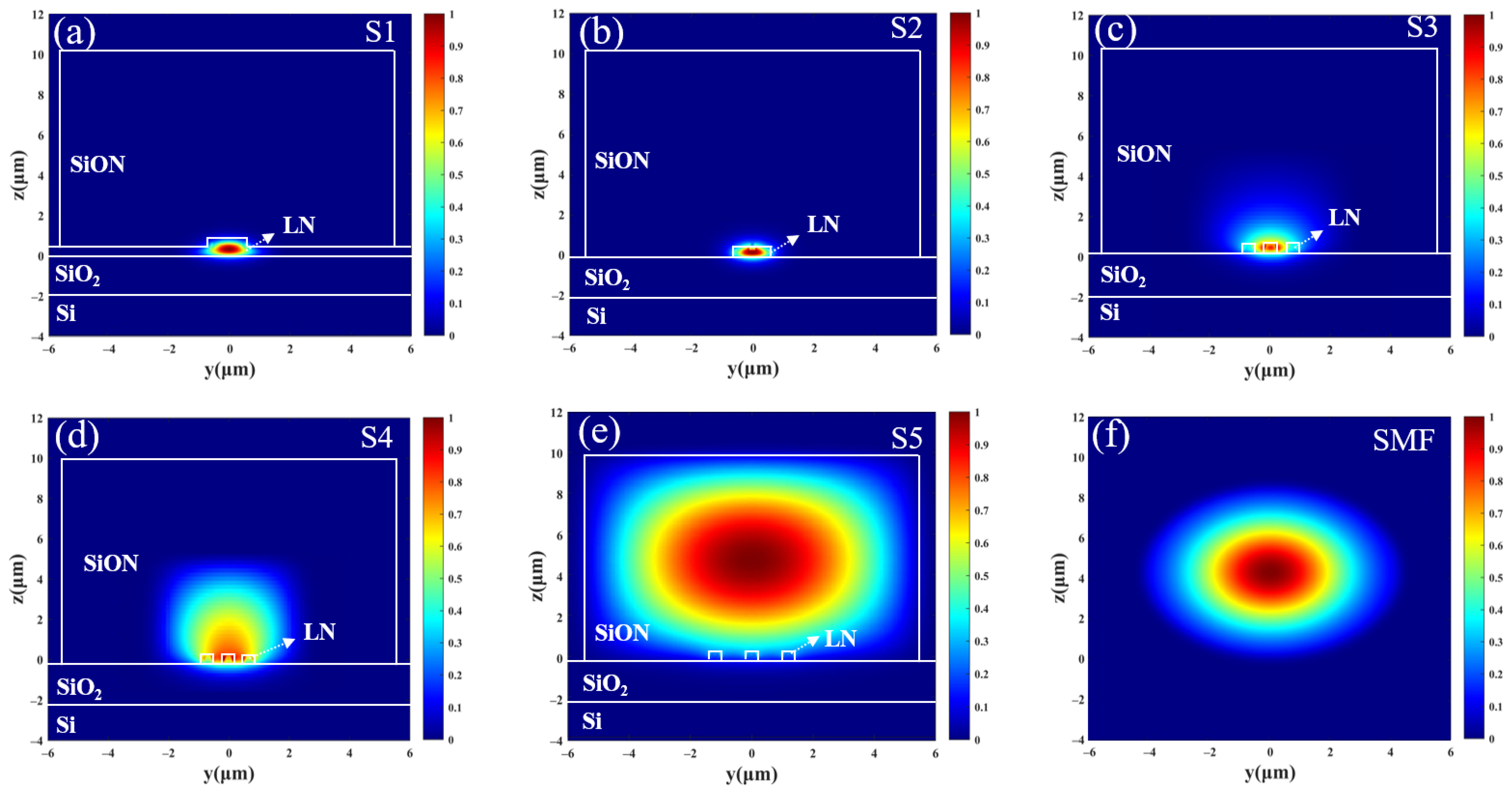
Figure 2a–e display the distribution of the TE mode at various cross-sections of the coupler. S5 provides an illustration of the TE mode profile at the coupling end face, while S1–4 exhibit the TE mode distribution in different regions along the coupler. The process of mode coupling from the fiber to the chip can be divided into three primary phases. Initially, the optical field from an SMF couples into the SiON waveguide, which is matched in mode size. Subsequently, the 3D three-tip taper waveguides adiabatically couple the mode field from the SiON waveguide into the slab taper of the bilayer taper. Finally, the light undergoes a transition from the slab taper to the ridge taper and eventually into the ridge waveguide.
The coupler was fabricated on a 600 nm x-cut lithium niobate on insulator (2 μm buried oxide and 525 μm Si carrier) substrate, with SiON top cladding. The refractive indices adopted for the materials were 3.48 for Si, 1.44 for SiO2, 2.2 for LN, and 1.56 for SiON, respectively. The ridge waveguide has a width of 1.5 μm (wr) and etch depth of 300 nm (hr) on a 3 μm width (ws) slab, tailored to operate under single-mode conditions.
The design utilized SMF, operating at wavelengths of 1310 and 1550 nm. Notably, this high MFD fiber offers superior alignment tolerance in comparison to lensed fiber, proving cost-effective and straightforward in preparation. The mode field profile of the fiber is depicted in
Figure 2f.
The loss of a coupler encompasses absorption loss, scattering loss, mode overlap loss, and mode transmission loss. The broad spectrum of thin-film lithium niobate contributes to minimal absorption loss. Additionally, in the simulation results, the waveguide sidewalls are assumed to be perfectly smooth, leading to the elimination of scattering loss. As a result, the primary focus of the discussion in this paper revolves around mode overlap loss and mode transmission loss.
The overall coupling efficiency when coupled with an SMF can be defined by the following equation:
Here, 𝜂 represents the overall coupling efficiency from the SMF to the coupler. 𝜂
1 signifies the mode overlap efficiency between the fundamental fiber mode and the delocalized mode at the chip facet, while 𝜂
2 expresses the mode transformation efficiency [
31].
When one mode is dominant, the mode overlap efficiency 𝜂
1 can be given as follows [
32]:
Here, E1 and E2 represent complex electric field amplitudes of the delocalized mode at the chip facet and fiber mode, respectively.
The mode transformation efficiency 𝜂2 quantifies the extent of light transformation from the chip facet to the three-tip taper waveguides in LNOI. This efficiency is determined by the lengths and widths of the tapers within the bilayer inversely tapered waveguide section and the multi-tip waveguide sections.
In addition to coupling efficiency, another critical parameter is the coupling loss, which denotes the amount of energy lost during transmission. It is typically calculated as follows [
33]:
Here, CL represents the coupling loss, and 𝜂 denotes the coupling efficiency.
Based on theoretical analysis, enhancing the performance of the coupler correlates with increased mode overlap efficiency (𝜂
1) between the fiber and the waveguide. Achieving higher mode transformation efficiency (𝜂
2) necessitates gradual variation in the taper’s geometry. While an ideal device should have a small footprint and high 𝜂
2, there exists a tradeoff between increasing 𝜂
2 and maintaining a compact device size. However, optimizing these parameters is complex due to the numerous design variables. Moreover, our design objectives encompass several criteria, such as achieving high 𝜂 and broad optical bandwidth (Δλ), accommodating large misalignment tolerances, and maintaining a small footprint. To address these design goals effectively, we implemented the particle swarm optimization (PSO) algorithm to automatically search for practical structural values [
31].
3. Simulation and Discussion
We investigated mode overlap efficiencies and mode transformation efficiency for the TE/TM mode using FDM instead of the time-consuming 3D finite difference time domain (FDTD) method. We find that the difference in simulated 𝜂 was less than 2% between the FDM and FDTD simulations [
29]. Despite the generally acknowledged higher accuracy in the latter numerical method, the FDM demonstrated significantly lower computational costs compared to the FDTD approach. Specifically, the simulation of mode overlap between the fiber and edge coupler facet employed the FDM, while the simulation of mode transformation along the coupler utilized the fully vectorial 3D EME solver.
3.1. Mode Overlap Efficiency Optimization
The approach to enhance coupling efficiency involves augmenting the optical field within the waveguide since the mode field in the fiber remains fixed and unchangeable. As the size of the tip waveguide diminishes, light confinement within the waveguide weakens, leading to an expansion in the optical field beyond the waveguide’s dimensions. To bolster the mode field within the waveguide, we adopted 3D inverted tapered structures. In contrast to a single-tip edge coupler, the 3D multi-tip edge coupler allows greater flexibility in horizontal and vertical adjustments. Through parameter optimization of these tips, we manipulate the distribution of the optical field within the waveguide to maximize alignment with the optical field in the optical fiber. This optimization aims to enhance coupling efficiency.
We employed the FDM method to optimize the parameters of the CLDWG, as well as the widths, heights, and gaps of the tips to attain the highest efficiency (𝜂
1). The optimization process involved fixing four parameters—
CLDW,
CLDH,
𝑤4,
h2, and
𝑔2—while varying the fifth one to observe the efficiency variations. Each parameter was individually swept, and the results are presented in
Figure 3a–e, respectively.
To achieve an ideal output mode field, an adjustment in the cladding at the output end was necessary. Despite the cladding thickness being 800 nm in other parts of the chip, fine-tuning the cladding dimensions was essential for better alignment between the output mode field and the fiber mode field. As depicted in
Figure 3a,b, when the cladding size is small, the mode field fails to spread adequately, resulting in higher coupling losses with single-mode fibers. With an increase in cladding size, the diffused waveguide mode field expands, leading to a reduction in coupling losses. Nevertheless, as the cladding size reaches a certain threshold, the control over the shape of the waveguide mode field diminishes, and a trend of decreasing coupling efficiency with single-mode fibers emerges.
Figure 3a,b demonstrate that setting the cladding thickness to 10 μm and the width to 11 μm minimized the coupling loss between the output mode field and the fiber mode field to approximately 0.18/0.16 dB of TE/TM mode.
Figure 3c illustrates that as
w4 increases, the optical mode field becomes more confined within the waveguide, exacerbating the mismatch between the waveguide and fiber mode fields, consequently leading to increased coupling loss. Within the
𝑤4 < 0.4 μm range, the difference in coupling loss is negligible. Considering the existing process precision [
11], a value of
𝑤4 = 0.15 μm is deemed suitable.
The findings from
Figure 3d highlight that optimizing the waveguide height parameter, specifically selecting
h2 = 0.14 μm compared to the conventional facet coupler with a waveguide facet height of 0.3 μm, results in a reduction of approximately 0.12/0.16 dB for TE/TM mode in facet coupling loss. This reduction is credited to the decreased longitudinal dimension, enabling a smaller waveguide size and facilitating greater optical mode field diffusion into the cladding. Consequently, this enhancement improves matching with the fiber mode field, thus lowering coupling loss.
Observing
Figure 3e, it is noted that the minimum coupling loss for TE mode occurs at
𝑔2 = 1.2 μm. The minimum coupling loss of 0.0382/0.049 dB for TE/TM mode is achieved under the conditions of
CLDW = 11 μm,
CLDH = 10 μm,
𝑤4 = 150 nm,
h2 = 140 nm, and
𝑔2 = 1.2 μm. As the parameters of the tip waveguides have been determined, further optimization of the mode transformation efficiency 𝜂
2 is explored in the subsequent section.
3.2. Mode Transformation Efficiency Optimization
The parameters 𝑤1, 𝑤2, 𝑤3, 𝑔1, h1, L1, L2, L3, and L4 governing the three-tip taper waveguides and the bilayer inversed taper are optimized using the EME simulation method. These parameters are treated as independent variables in the optimization process.
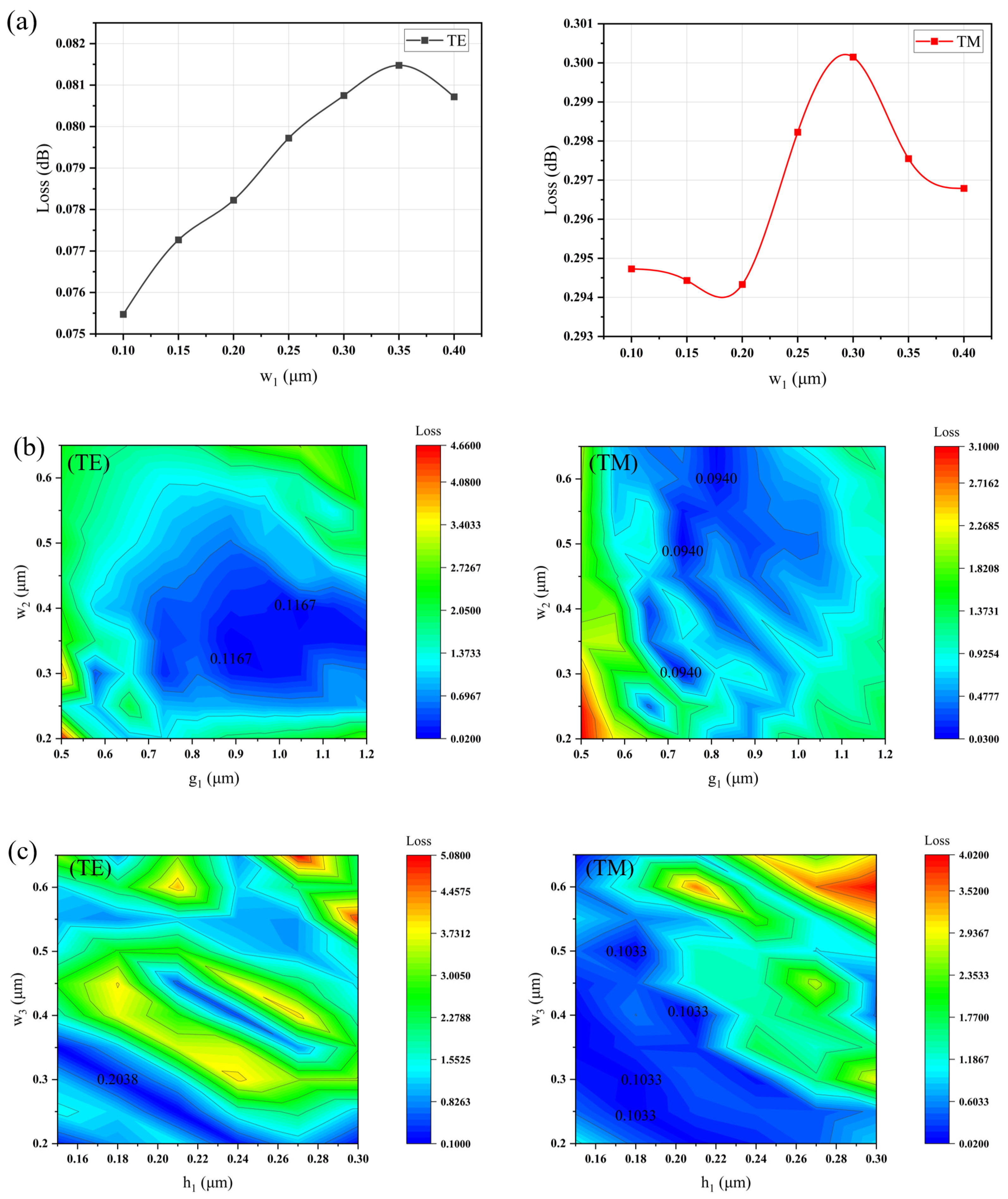
The PSO algorithm concurrently optimizes 𝑤1, 𝑤2, 𝑤3, 𝑔1, and h1. Starting with initial values of 100 μm for L1, L2, L3, and L4, the figure of merit (FOM) defined as the transmission loss is minimized. PSO employs 10 generations with a swarm size of 10, resulting in 100 simulations in a search for the minimum transmission loss for TE mode within a three-dimensional space. The optimized initial values for 𝑤1, 𝑤2, 𝑤3, 𝑔1, and h1 obtained from PSO are 0.1, 0.35, 0.20, 0.89, and 0.25 μm, respectively, serving as the starting values for subsequent simulations.
Individual parameter sweeps are conducted one by one while maintaining the other parameters at their initial values. The sweep for
𝑤1 spans from 0.1 to 0.4 μm, and the resulting transmission loss at a wavelength of 1.55 μm is depicted in
Figure 4a. Considering fabrication precision [
11],
𝑤1 is set at 0.12 μm, aiming for decreased mode transform loss during the mode conversion from the upper ridge taper to the lower slab taper.
Similar optimization sweeps are performed for the parameters
𝑤2,
𝑤3,
𝑔1, and
h1. Notably, considering the interdependence among parameters
𝑤2,
𝑔1, and
𝑤3,
h1, a nested parameter scan is applied, as illustrated in
Figure 4b,c. Based on the optimization outcomes, the selected values are
𝑤2 = 0.35 μm,
𝑤3 = 0.20 μm,
𝑔1 = 0.89 μm, and
h1 = 0.25 μm.
Under the given conditions, a series of scans are performed using the “propagation sweep” function within the EME method, targeting the lengths of the four taper sections individually. Initially, with
L2,
L3, and
L4 set at constant values of 300 μm, considered sufficiently large lengths, the scan focuses on
L1. As illustrated in
Figure 5a, it is observed that the transmission efficiency of the TE mode stabilizes after reaching
L1 > 50 μm, and for TM mode,
L1 needs to reach 60 μm.
Following this, with
L1,
L3, and
L4 held constant at 50, 300, and 300 μm, respectively, another scan is conducted, this time for
L2. The outcomes depicted in
Figure 5b indicate that the mode transmission efficiency stabilizes after
L2 exceeds 200 μm.
Utilizing similar methodology, scans and optimizations are performed separately for
L3 and
L4, as illustrated in
Figure 5c,d, respectively. Considering the balance between transmission efficiency and device size, the final optimal values are determined as
L1 = 50 μm,
L2 = 200 μm,
L3 = 200 μm, and
L4 = 150 μm. By employing sufficiently large lengths, the waveguide’s width undergoes a gradual change over an extended distance, facilitating the adiabatic transition of the mode from the ridge waveguide to the slab waveguide and its continued transition within the slab waveguide.
The optimized parameters for the edge coupler are compiled and presented in
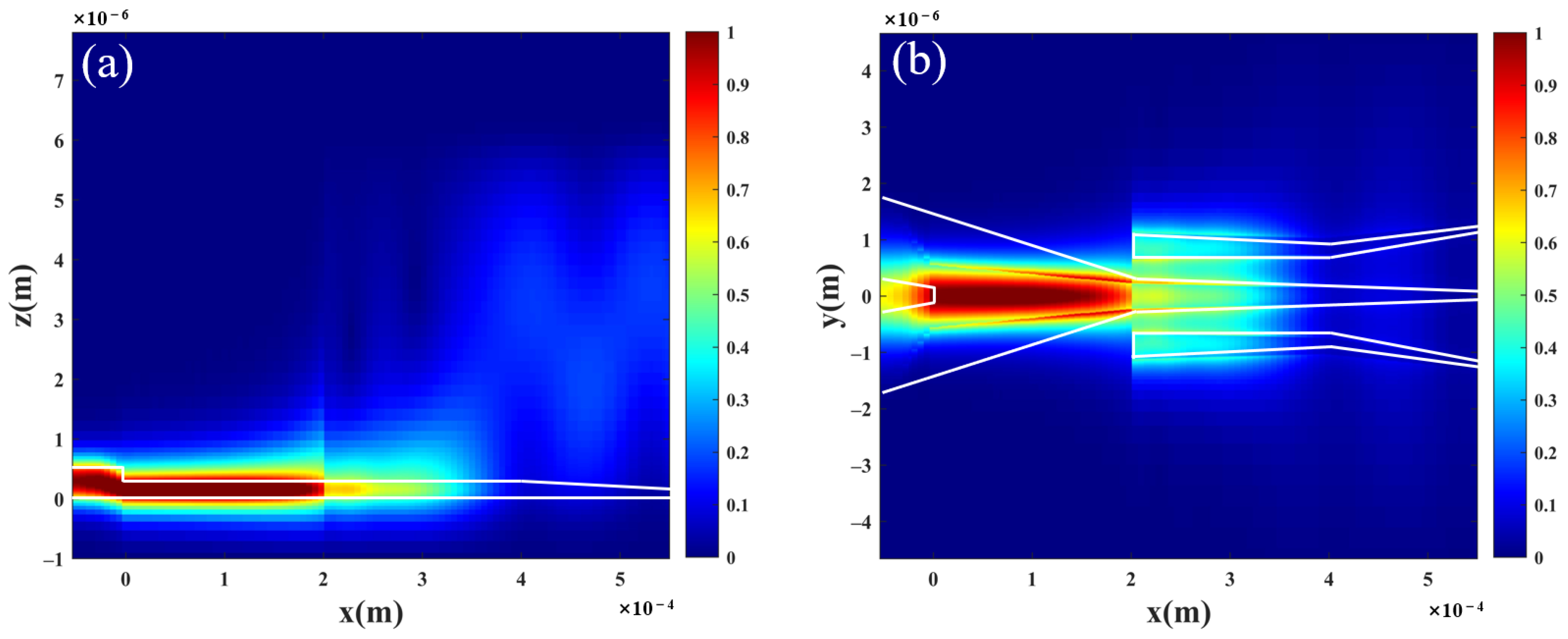
Table 1. With the designed parameters, the adiabatic tapers achieved a minimal mode transformation loss of 0.03/0.0468 dB of TE/TM mode. The simulation of the light field distribution in the edge coupler of TE mode, based on these parameters, is depicted in
Figure 6. The results demonstrate the compression of the visible mode field into the lower 2 μm slab initially, followed by a gradual spreading due to the taper’s narrowing, culminating in a larger mode field distribution area through the triple-tip adiabatic reverse-tapered waveguide. The anticipated design loss stands at approximately 0.0682/0.0958 dB TE/TM mode.
3.3. Misalignment Tolerance and Fabrication Tolerance
In practical applications, alignment errors between the optical fiber and the coupler are expected due to stage movement inaccuracies.
Figure 7 illustrates the overall coupling loss at a wavelength of 1.55 μm for the three-tip edge coupler, concerning misalignment in both the horizontal (Y) and vertical (Z) directions. For TE mode, the misalignment tolerance for 1 dB loss penalty is ±1.62 μm in the horizontal direction, and in the vertical direction, the misalignment tolerance for 1 dB loss penalty is ±1.73 μm. For TM mode, the misalignment tolerance for 1 dB loss penalty is about ±1.76 and ±1.74 μm in the horizontal and vertical direction, respectively. Such misalignment tolerances in both horizontal and vertical directions are easily achievable by the modern alignment technique.
The device’s sizable alignment tolerance greatly facilitates testing, enhancing test stability. The presence of multiple tips in the structure results in an expanded energy distribution of the mode field along the horizontal axis. When the fiber undergoes horizontal shifting, this design amplifies the overlap between the mode field in the fiber and that in the tip waveguide, thereby increasing the alignment tolerance to a certain extent.
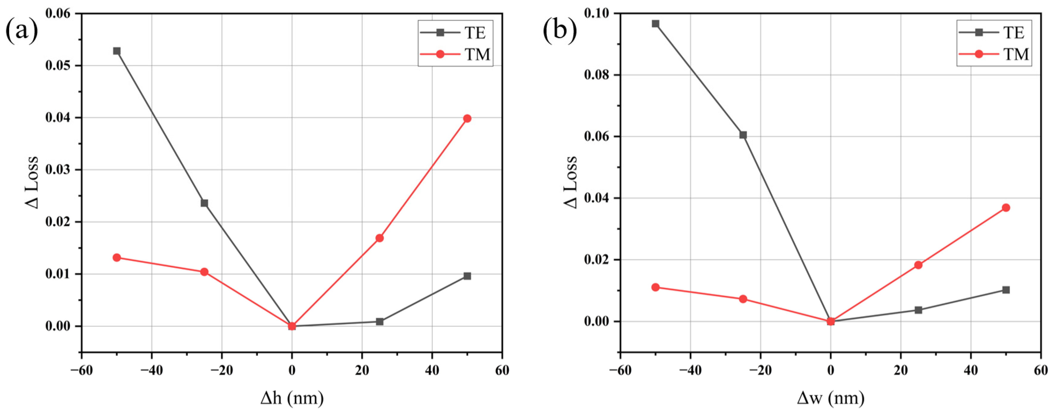
We also investigated the tolerance in the fabrication of the proposed coupler. Here, the fabrication tolerance of the devices is numerically analyzed by changing the etching depth (
h2) and the width of the tip (
w4). In micro- and nanofabrication processes, fabrication errors are usually less than 50 nm. Positive signs (+) denote fabrication sizes larger than the designed size, while negative signs (−) indicate smaller sizes. The results are depicted in
Figure 8. For the three-tip edge coupler, the coupling loss remains below 0.06 dB for 𝛥
h = ±50 nm and is less than 0.10 dB for 𝛥
w = ±50 nm of TE mode. For TM mode, the variation in loss of the device is less than 0.04 dB for every 50 nm change in 𝛥
h and 𝛥
w. These outcomes suggest that the proposed device exhibits a commendable tolerance to fabrication variations.
3.4. Wavelength Dependence
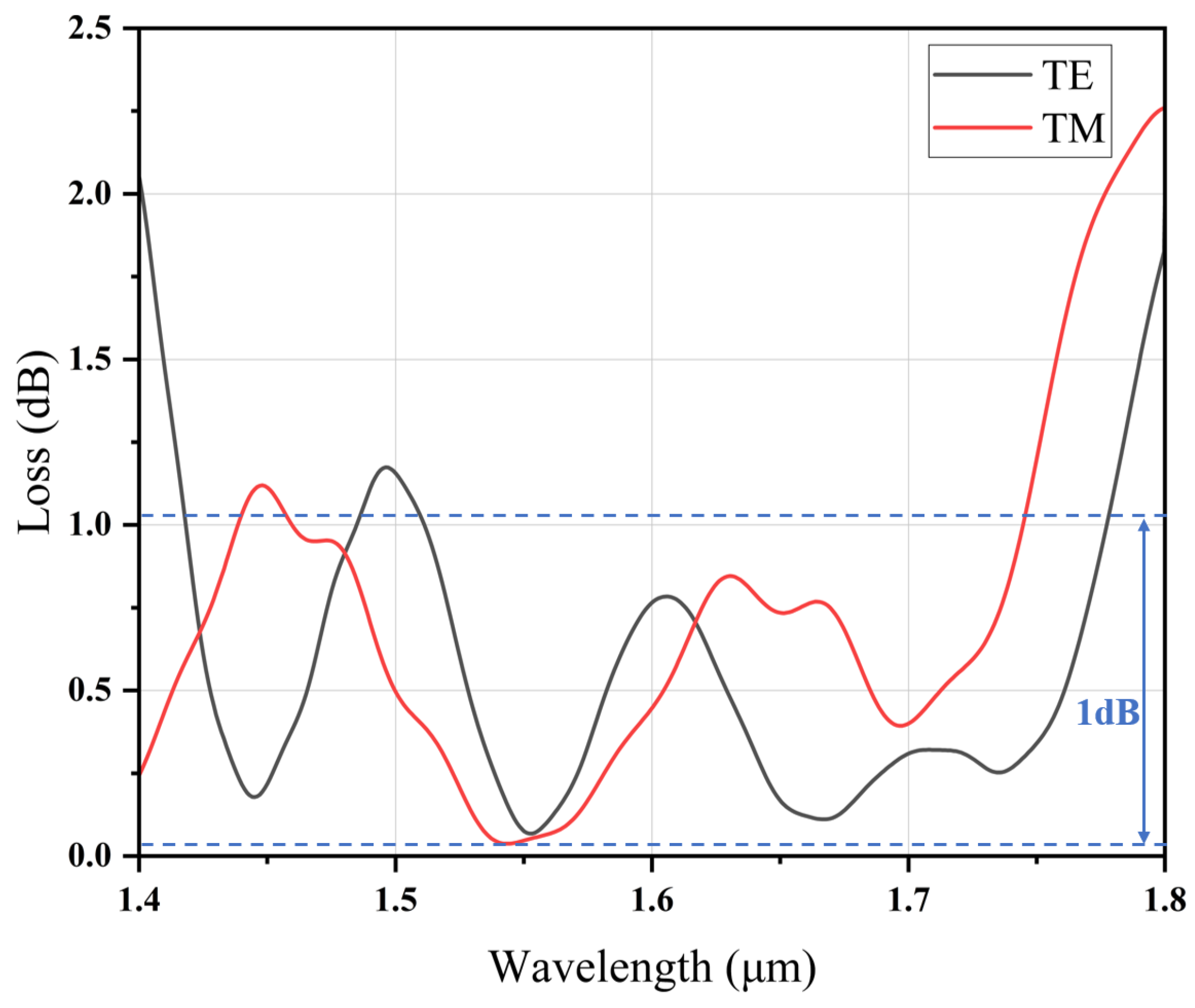
We conducted simulations to assess the wavelength dependency in the overall coupling efficiency between the coupler and SMF, represented in
Figure 9. For the TE mode, 1 dB bandwidth is 270 nm, achieved between 1509 and 1779 nm. For the TM mode, the 1 dB bandwidth is 288 nm, ranging from 1457 to 1745 nm. The results indicate superior overall coupling efficiency at longer wavelengths. An important observation is the slight oscillation in the overall coupling efficiency of the four-tip edge coupler, attributed to the Fabry–Pérot resonance between the end faces of the multi-tip edge coupler.
Table 2 gives the comparison of the coupling performance between the proposed edge coupler in this paper and other structures. Our work differs significantly from other studies in that we designed a multi-tapered 3D edge coupler on the LNOI platform. The width and height of the waveguide both changed, introducing more variables for optimization in both horizontal and vertical directions, allowing for a more extensive expansion of the mode field area. This facilitates low-loss coupling with optical fibers of larger mode field sizes and increases misalignment tolerance. In contrast to couplers using only a single taper [
22,
24,
28], our coupler demonstrates superior coupling performance with optical fibers of bigger mode field sizes. Another notable distinction is our use of SiON cladding. By employing SiON cladding to control the dimensions and refractive index of the waveguide mode field, we enhance coupling efficiency, resulting in low-loss coupling with optical fibers.
4. Conclusions
We present a novel broadband, ultra-low-loss 3D multi-tip edge coupler designed on the LNOI platform for direct interfacing between the chip and SMF. This cutting-edge device incorporates SiON cladding, three 3D inversely tapered waveguides, and a double-layer reverse waveguide. Optimized parameters and the SiON cladding design enhance the alignment between the waveguide mode field and the fiber mode field. Through FDM-optimized tip heights, widths, and gaps, we achieved minimized facet coupling losses. Additionally, leveraging EME, we optimized the coupler’s length to reduce mode transmission losses. As a result, the total coupling loss is significantly reduced to 0.0682/0.0958 dB/facet for TE/TM mode at 1550 nm. Significantly, this structure exhibits remarkable mode overlap efficiency with a standard 8.2 μm MFD SMF, ensuring a 1 dB bandwidth of 270 and 288 nm for TE and TM mode. Notably, this device showcases a high misalignment tolerance and remarkable tolerance to fabrication variations. The misalignment tolerance for 1 dB loss penalties of TE mode along the Y and Z directions are ±1.62 and ±1.73 μm, respectively. For TM mode, the penalties are ±1.76 and ±1.74 μm along the Y and Z directions. Taking into account the fabrication process, the coupling loss of TE mode remains below 0.09 dB for 𝛥w = ±50 nm and below 0.05 dB for 𝛥h = ±50 nm, indicating excellent manufacturing tolerance. For TM mode, the loss remains below 0.04 dB for every 50 nm change in 𝛥h and 𝛥w. This low-loss, high-bandwidth edge coupler demonstrates exceptional potential and competitiveness for fiber-to-chip edge coupling applications within the realm of lithium niobate photonics.

