Article

Calibration of Waveplate Retardance Fluctuation Due to Field-of-View Effect in Mueller Matrix Ellipsometer

State Key Laboratory for Digital Manufacturing Equipment and Technology, Huazhong University of Science and Technology, Wuhan 430074, China
*
Author to whom correspondence should be addressed.
Photonics 2023, 10(9), 1038; https://doi.org/10.3390/photonics10091038
Submission received: 18 August 2023 / Revised: 8 September 2023 / Accepted: 9 September 2023 / Published: 12 September 2023
(This article belongs to the Special Issue Advanced Polarimetry and Polarimetric Imaging)

Abstract

:
Leveraging their unique phase modulation characteristics, birefringent waveplates have been widely used in various optical systems. With the development of material science and manufacturing techniques, the polarization properties of waveplates have become increasingly complex and diverse. Among these properties, the field-of-view effect of the waveplate caused due to manufacturing defects or improper installation procedures is extremely difficult to calibrate and seriously affects the precision and accuracy of the relevant optical systems. In this paper, a calibration method that can compensate for the field-of-view effect of waveplates installed in the instrument is proposed. Moreover, to approve the fidelity of the proposed calibration method, a series of film thickness measurement experiments are carried out. The results show that under different installation conditions of the waveplates, the precision and accuracy of the film thickness measured with the proposed method significantly improved. This method can be expected to reduce the assembly difficulty of such optical systems, while also improving their accuracy and stability.

1. Introduction

The waveplate is one of the most commonly used optical components in optical systems. It can produce an additional optical path difference (or phase difference) between two mutually perpendicular light components. Thanks to its unique polarization modulation characteristics, the waveplate has been widely used in various optical systems, such as interferometry [1,2], polarimeter/ellipsometry [3,4,5,6,7,8,9], birefringent filters [10,11], etc. Meanwhile, with the development of material technologies, the materials of waveplates are no longer limited to traditional quartz, and cover a much wider and richer range, including gypsum, LiTaO3, ZnO, etc. [12,13,14,15]. This enables waveplates to exhibit complex and diverse polarization characteristics, while also increasing the difficulty in the characterization and calibration of their polarization properties. Therefore, the accurate polarization property calibration [16,17,18,19] of the waveplate plays an important role in improving the accuracy and stability of the relevant optical instruments.
In previous studies, it was observed that the retardance of a birefringent waveplate fluctuated significantly when the incident angle of the light and the azimuth of the waveplate varied at the same time. This phenomenon existing in the waveplates is called the field-of-view effect [20,21]. While the field-of-view effect of waveplates has been utilized for applications such as attitude angle tracking [20], the loss of precision and accuracy it causes in other optical systems that rely on waveplates for phase modulation is unacceptable. Therefore, it is of great importance to calibrate and compensate for the retardance fluctuation caused by the field-of-view effect of waveplates in optical systems.
There are many researchers dedicated to investigating the relationship between the incident angle of light and the retardance of waveplates using ellipsometry [21,22,23]. West and Smith have comprehensively studied the errors associated with birefringent waveplates, including the thickness error, field-of-view errors, optic axis tilt errors and misalignment. They developed a piece of equipment consisting of three Glan–Thompson polarizers, a Soleil–Babinet compensator, a multiline He–Ne laser source and a photomultiplier tube detector to measure the absolute retardance of the waveplate [24]. These studies clearly exhibit the significant influence of the incident light angle on the retardance of waveplates. Ruder et al. [25] used dual continuously rotating anisotropic mirrors to construct a single-wavelength Mueller matrix ellipsometer in a normal transmission configuration. However, few studies have investigated how to calibrate the system when the incident light is tilted with respect to the waveplate. This may be a limitation to improving the precision and accuracy of high-precision optical systems.
In this paper, a calibration method for compensating for the field-of-view effect of waveplates in optical systems is proposed. Firstly, a characterization model of the field-of-view effect in waveplates is proposed. Subsequently, a series of tilt angle measurement experiments are carried out. The consistency between the simulated attitude angles of waveplates and the measured tilt angles demonstrate the correctness and the effectiveness of the proposed method. In addition, the proposed characterization model is applied into the calibration of a single-wavelength Mueller matrix ellipsometer (SWE). Compared to the measured thicknesses on a set of standard SiO2 thin films given using a commercial MME, the deviations decreased from 6.5% to 1.8% with the field-of-view error considered. It is expected that the proposed calibration method can improve the accuracy and precision of the instrument, while also reducing the difficulty of the instrument assembly.

2. Characterization of the Waveplate

The polarization state of the light passing through the compensator can deviate from the theoretical expectation due to the design and manufacturing defects, as well as unsatisfactory installations. Generally speaking, the waveplates exhibit small depolarizations due to manufacturing defects, so the characterization of practical waveplates at the azimuth θ can be expressed using the flowing Mueller matrix formalism:
M C ( δ , θ , b , c ) = R ( θ ) M C ideal ( δ ) M Dep ( b , c ) R ( θ ) ,
where M C ideal is the Mueller matrix of the ideal compensator, and can be represented as [26]:
M C ideal = 1 0 0 0 0 1 0 0 0 0 cos ( δ ) sin ( δ ) 0 0 sin ( δ ) cos ( δ ) ,
where δ denotes the retardance of the compensator. MDep is the Mueller matrix of the depolarization effect in the waveplates, and can be expressed as [27]:
M Dep = 1 0 0 0 0 1 c 0 0 0 0 1 b 0 0 0 0 1 b ,
where b and c are the linear depolarization parameters of the compensator. R(θ) is the Chandrasekhar matrix that can unify the optical axis direction of each optical component to the incident plane reference system, and its matrix form can be denoted as:
R ( θ ) = 1 0 0 0 0 cos ( 2 θ ) sin ( 2 θ ) 0 0 sin ( 2 θ ) cos ( 2 θ ) 0 0 0 0 1 ,
In this paper, a compound zero-order waveplate was selected as the compensator to study the retardance fluctuation introduced as a result of the field-of-view effect. The compound zero-order waveplate was composed of two multiorder single waveplates composed of quartz, whose optical axes were oriented perpendicular to each other, as shown in Figure 1. Without losing generality, we assumed that the optical axis of the thicker multiorder single waveplate was parallel with the x-axis, and that of the thinner one was parallel with the y-axis. According to the above descriptions and derivations, the retardance of the compound zero-order waveplate under an arbitrary incidence and azimuth could be calculated using [21,28,29].
δ ( θ tilt , β ) = 2 π λ L = 2 π λ i = 1 2 d i ( n y i 2 sin 2 θ tilt n z i 2 sin 2 θ tilt ) = 2 π λ d 1 ( n e 2 n e 2 cos 2 β + n o 2 sin 2 β n o 2 sin 2 θ tilt n o 2 sin 2 θ tilt ) 2 π λ d 2 ( n e 2 n e 2 sin 2 β + n o 2 cos 2 β n o 2 sin 2 θ tilt n o 2 sin 2 θ tilt ) ,
where θtilt is the tilt angle of the waveplate, which is defined as the angle between the incident light and the normal direction of the waveplate’s surface. Additionally, β is the fast axis azimuth angle, d1 and d2 are the thicknesses of the thicker single waveplate and the thinner single waveplate, respectively, and ne and no are the extraordinary index and the ordinary index of the quartz, respectively.
The dispersion equation (Schott dispersion formula) was:
n o 2 = a 0 o + a 1 o λ 2 + a 2 o λ 3 + a 3 o λ 4 + a 4 o λ 5 + a 5 o λ 6 n e 2 = a 0 e + a 1 e λ 2 + a 2 e λ 3 + a 3 e λ 4 + a 4 e λ 5 + a 5 e λ 6 ,
where aio and aie (i = 1, …, 5) are the ordinary dispersion coefficient and the extraordinary dispersion coefficient, respectively, which can be found in the material libraries of most manufacturers. λ is the wavelength of the incident light. It could be calculated that ne = 1.5517, no = 1.5426 when the material was quartz and the wavelength was 632.8 nm. It could be seen from the data provided by the manufacturer that the total thickness of the quartz biplate (including the air gap ≈ 203.200 μm) was approximately 2177.990 μm. According to Equation (5), we could obtain the effective thickness (i.e., the difference between the thicknesses of the two multiorder single waveplates for a compound zero-order biplate) of the biplate, amounting to 17.480 μm, and the designed thicknesses of the two single waveplates were d1 = 996.135 μm and d2 = 978.655 μm. Therefore, the initial field-of-view parameters could be determined with these conditions. Figure 2 shows the simulation results of the retardance fluctuation versus the azimuth at different waveplate tilt angles.

3. System and Calibration Method

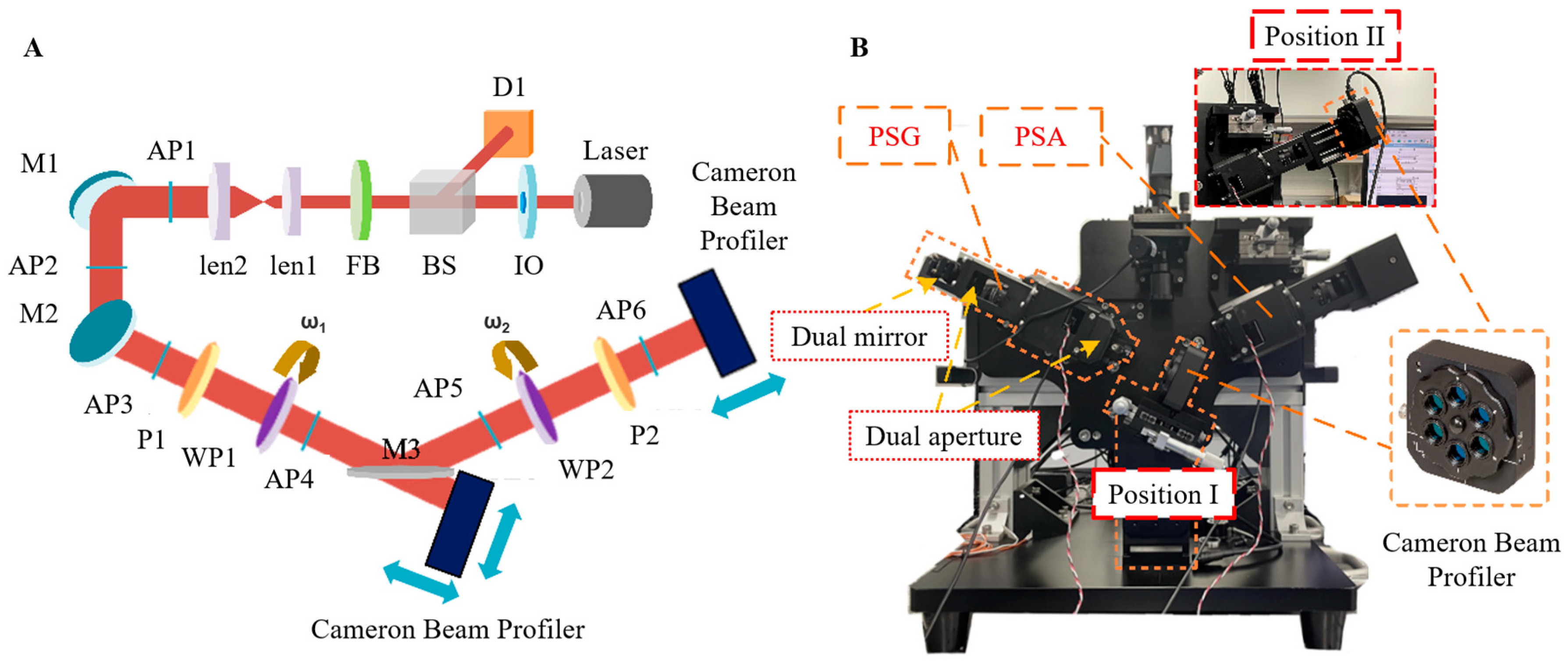
3.1. Single-Wavelength Mueller Matrix Ellipsometer System

The instrument is a self-developed SWE, which could measure 16 Mueller matrix elements simultaneously. As schematically shown in Figure 3, the SWE consisted of three parts: a CW He–Ne laser (HRS015B 100-240VAC, Thorlabs, Newton, NJ, USA), a polarization state generator (PSG) and a polarization state analyzer (PSA). The laser first transmitted through an optical isolator (IO-2D-633-VLP, Thorlabs, Newton, NJ, USA), which prevented the interference of the reflected light. A beam (BS025, Thorlabs, Newton, NJ, USA) split the laser into two beams with a 1:9 intensity ratio. One beam entered detector1 (PDA36A2, Thorlabs, Newton, NJ, USA) directly to monitor the intensity fluctuation of the light source, while the other entered the main optical path. After passing through a bandpass filter (FLH633-5, Thorlabs, Newton, NJ, USA) and being reflected on a mirror (64-013, Edmund, Barrington, NJ, USA), the light would incident on a sample through the PSG at an angle of 65 degrees. The PSG consisted of a polarizer (LPVISC100-MP2, Thorlabs, Newton, NJ, USA) and a waveplate (WPQ10M-633, Thorlabs, Newton, NJ, USA). The PSA then modulated the sample-reflected light, which would eventually be captured by detector2 (PDA36A2, Thorlabs, Newton, NJ, USA). The PSA consisted of a waveplate and a polarizer. The two detachable focus lenses installed in the PSG and PSA could reduce the size of the light spot when the size of the measured sample was very small. The self-developed instrument could obtain the full Mueller matrix of the sample using the above configuration. A high-precision data acquisition card (USB6281, NI, Austin, TX, USA) was required to meet the criteria of the high-precision real-time measurement.
Generally speaking, the detected light intensity matrix Idec could be modeled as the product of the modulation matrix G of the PSG, the Mueller matrix MS of the sample and the demodulation matrix A of the PSA [30]:
I dec = A M S G ,
Let us denote the 4 × 4 Mueller matrix of the sample as:
M S = m i , j 4 × 4 , ( i , j = 1 , 2 , 3 , 4 ) ,
The modulation matrix G and demodulation matrix A could be represented as:
G = S PSG 1 S PSG 2 S PSG k S PSG K ,
A = H PSA 1 H PSA 2 H PSA k H PSA K ,
where S PSG k and H PSA k are the kth Stokes vector of the polarized light output from the PSG and PSA, respectively. K is the number of the total sampling point in an optical cycle.
According to the optical path of the SWE, the kth Stokes vector S PSG k and H PSA k could be calculated with Equations (11) and (12), respectively [30]:
S PSG k = R C 1 k M C ( δ 1 k , b 1 , c 1 ) R C 1 k R P M P ( D t 1 , δ P ) R P S in ,
H PSA k = 1 0 0 0 R A M A ( D t 2 , δ A ) R A R C 2 k M C ( δ 2 k , b 2 , c 2 ) R C 2 k ,
where P and A are the azimuth angle of the polarizer and the analyzer in the PSG and PSA, respectively. The δP and δA are the weak birefringence retardances of the polarizer and analyzer, respectively. The first and second compensators were driven using two servo hollow motors (AgilityRH, Applimotion, Loomis, CA, USA), and their fast axis azimuth was changed according to the following relations: C 1 k = ω1tk + C 1 initial and C 2 k = ω2tk + C 2 initial . C 1 initial and C 2 initial are the initial azimuths of the compensators. ω1 and ω2 are the rotation speed of the first and second compensators, respectively. Additionally, the rotation ratio of ω1 and ω2 was set to 1:5 in our instrument.
The actual Mueller matrix of the polarizer and analyzer could be shown as [31,32]:
M P / A ( D t , δ P / A ) = 1 D t 0 0 D t 1 0 0 0 0 2 cos ( δ P / A ) 1 D t 2 2 sin ( δ P / A ) 1 D t 2 0 0 2 sin ( δ P / A ) 1 D t 2 2 cos ( δ P / A ) 1 D t 2 ,
where Dt is the extinction parameter, which represents the ratio of the difference between the transmittance of the p-polarized light and the s-polarized light passing through the polarizer to the sum of the transmittances of the two polarization components:
D t = I p I s I p + I s ,

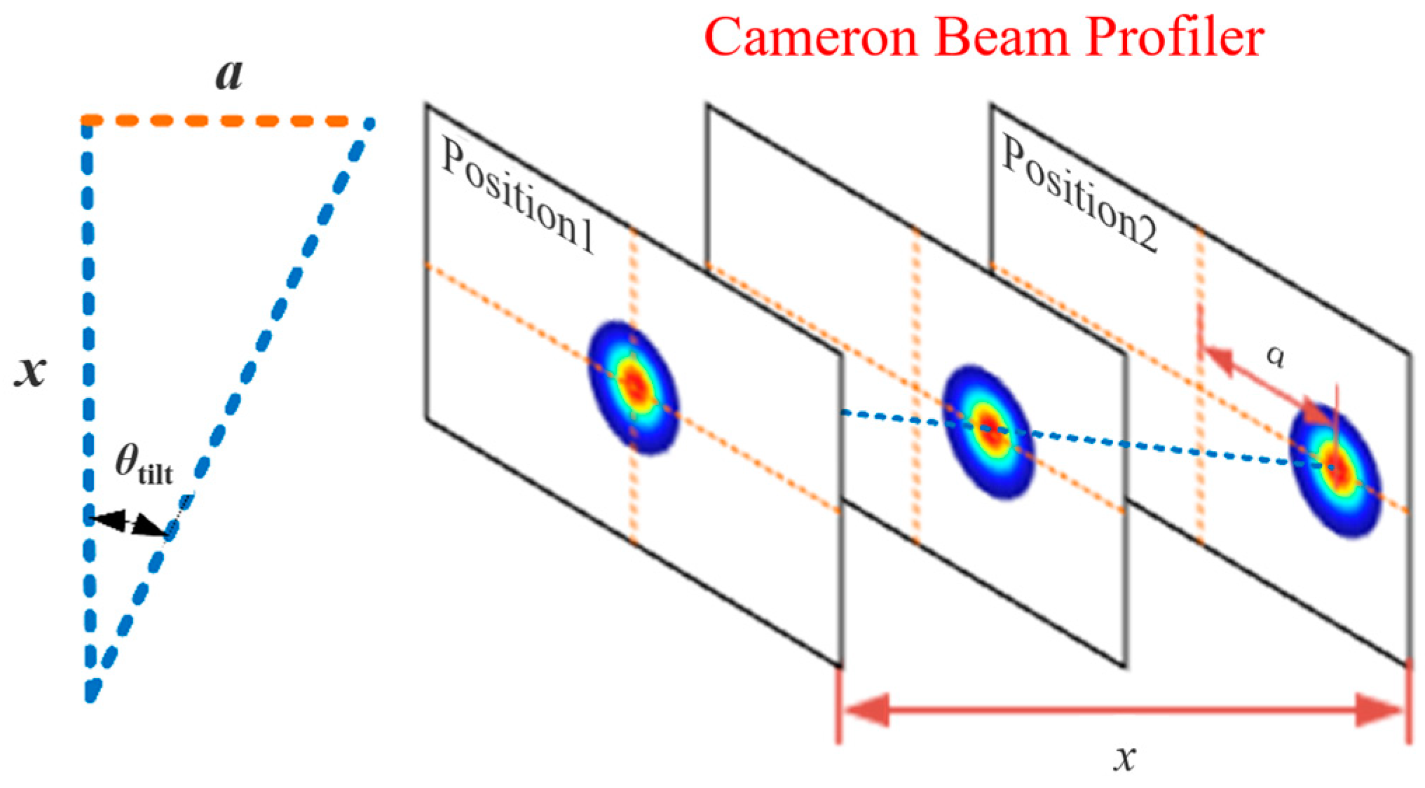
3.2. Calibration of the Waveplate Retardance Fluctuation

As observed in Section 2, the retardance of the compound zero-order waveplate varied sinusoidally with the azimuth, and the fluctuation amplitude increased with a greater tilt angle. To prevent an inaccurate calibration caused due to systematic parameter coupling, Equations (15) and (16) could substitute the waveplate characterization model from Section 2 when performing the regression calibration using the Levenberg–Marquardt algorithm.
δ 1 k = A C 1 sin ( ω 1 t k + ϕ C 1 ) + δ C 1 center ,
δ 2 k = A C 2 sin ( ω 2 t k + ϕ C 2 ) + δ C 2 center ,
where AC1 and AC2 are the retardance amplitudes of the first and second compensators, respectively. ϕC1 and ϕC2 are the azimuth angles of the waveplates. The δ center C1 and δ center C2 are the central retardances of the first and second waveplate, respectively.
The instrument needed to be carefully calibrated to maintain high performance [33]. The instrument was calibrated with a series of standard SiO2 film samples. The theoretical Mueller matrices of the samples could be calculated from the refractive indices (n and k), the thicknesses d and the incidence angles θ of the measurements, while the measured Mueller matrices could be obtained with the SWE. In this case, the system parameters of the SWE that needed to be calibrated involved the azimuthal angles of polarizer P, analyzer A, the weak birefringence retardance δP and δA of the polarizer and analyzer, the extinction parameters Dt1 and Dt2, the initial azimuths C 1 initial and C 2 initial of the compensators, the retardance of the first and second compensators δ center C1 and δ center C2, the rotation speed of first and second compensators ω1 and ω2, the retardance amplitude of the first and second compensators AC1 and AC2, the azimuth angles of waveplates ϕC1 and ϕC2, the thicknesses d and the incidence angle θ, as well as the depolarization parameters of the first and second compensators b1, c1 and b2, c2. Moreover, the nonlinear parameters of the detectors a0, a1, a2 and a3 had to be considered, which could be defined with the characterization model of the detector’s nonlinear response [34]:
I out = α 0 + α 1 I in + α 2 I in 2 + α 3 I in 3 ,
where Iin is the input light intensity of the detector and Iout is the output signal value of the detector.
Therefore, the system parameter psys could be written in the vector form as:
p sys = [ P ,   D t 1 ,   δ P C 1 initial ,   ω 1 ,   δ   center   C 1 ,   A C 1 ,   ϕ C 1 ,   b 1 ,   c 1 ,   C 2 initial ,   ω 1 ,   δ   center   C 2 ,   A C 2 ,   ϕ C 2 ,   b 2 ,   c 2 ,   P ,   D t 1 ,   δ P ,   θ incident ,   d ,   a 0 ,   a 1 ,   a 2 ,   a 3 ] ,
With the cost function defined as Equation (19), the system parameter psys could be obtained from the measured light intensity Imeas by using the Levenberg–Marquardt algorithm [35].
p sys = arg min p sys Ω p I meas I calc ( p sys ) T Γ I meas + I meas I calc ( p sys ) ,
where Imeas is the actual measurement intensity matrix, Icalc is the theoretical intensity matrix, Ωp indicates the value range of the system parameters, Γ I meas + is the Moore–Penrose pseudoinverse of the covariance matrix of the measured intensity matrix. In addition, Γ I meas + = ( Γ I meas + · Γ I meas + ) 1 · Γ I meas T . The tilting-induced retardance error of the polarizer was ignored, since it usually varied within ±0.05° when the tilt angle was less than 5°, which was quite small compared with the field-of-view effect of the waveplate. The relative optical parameters in the corresponding defined ranges could be decoupled and extracted. It was noted that Equations (18) and (19) yielded values of P, Dt1, C 1 initial , ω1, δ center C1, AC1, ϕC1, b1, c1, C 2 initial , ω2, δ center C2, AC2, ϕC2, b2, c2, A and Dt2 in the ranges −180° ≤ P, A, C 1 initial , C 2 initial ≤ 180°, 0.95 ≤ Dt1, Dt2 ≤ 1, 80° ≤ δ center C1, δ center C2 ≤ 100°, 1438°/s ≤ ω1 ≤ 1442°/s, 7198°/s ≤ ω2 ≤ 7202°/s, −1 ≤ b1, c1, b2, c2 ≤ 1, 60° ≤ θincident ≤ 70°, 0 nm ≤ d ≤ 100 nm, −180° ≤ ϕC1, ϕC2 ≤ 180°, −10 ≤ AC1, AC2 ≤ 10, 0 ≤ a1 ≤ 2 and −1 ≤ a1, a2, a3 ≤ 1, respectively.
When the calibration was completed, the retardance sequence in an optical cycle could be obtained by substituting the system parameters AC1, AC2, ω1, ω2, δ center C1, δ center C2, ϕC1 and ϕC2 into Equations (15) and (16). The retardance sequence of C1 and C2 could be denoted as:
δ 1 / 2 = δ 1 / 2 1 δ 1 / 2 2 δ 1 / 2 3 δ 1 / 2 K ,
Similarly, utilizing the nonlinear regression fitting method, the parameters of the field-of-view errors hC = [θtilt, β, d1, d2] could be accurately determined.
h C = arg min h C Ω h δ meas δ calc ( h C ) T Γ δ meas + δ meas δ calc ( h C ) ,
where δmeas is the actual fitted retardance sequence of C1 and C2 calculated with Equation (21) and δcalc is the theoretical retardance sequence calculated with Equation (1); Ωh indicates the value range of the field-of-view error parameter hC, Γ δ meas + is the Moore–Penrose pseudoinverse of the covariance matrix of the actual fitted retardance sequence and Γ δ meas + = ( Γ δ meas + · Γ δ meas ) 1 Γ δ meas T . Then, the system parameter MS could be obtained from the following:
M S = arg min M S Ω M I meas I calc ( p sys , M S ) T Γ I meas + I meas I calc ( p sys , M S ) ,
where ΩM indicates the value range of the system Mueller matrix. Then, the thickness d of the sample could be obtained from the following:
d = arg min d Ω d M meas M calc ( a , d ) T Γ M meas + M meas M calc ( a , d ) ,
where Ωd indicates the value range of the thickness, a denotes the priori value of the reconstruction, Mmeas is the measurement Mueller matrix, Mcalc is the theoretical Mueller matrix and Γ M meas + is the Moore–Penrose pseudoinverse of the covariance matrix of the measured Mueller matrix, as well as Γ M meas + = ( Γ M meas + · Γ M meas ) 1 · Γ M meas T .

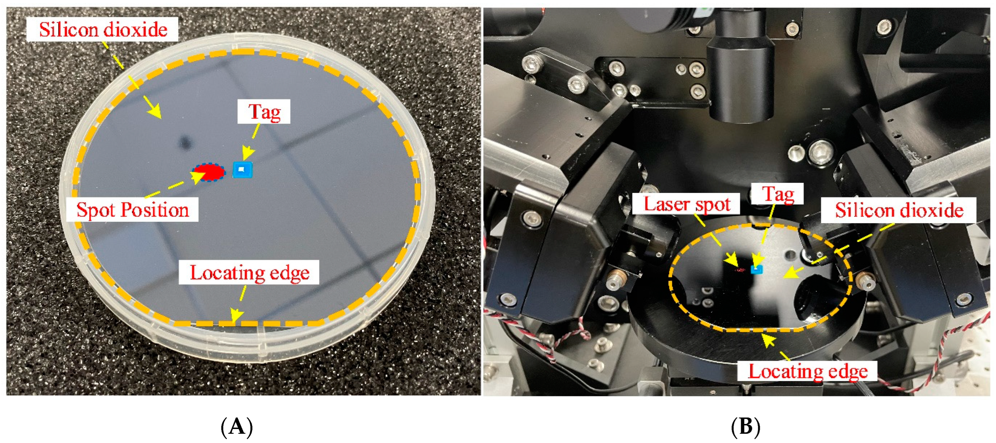
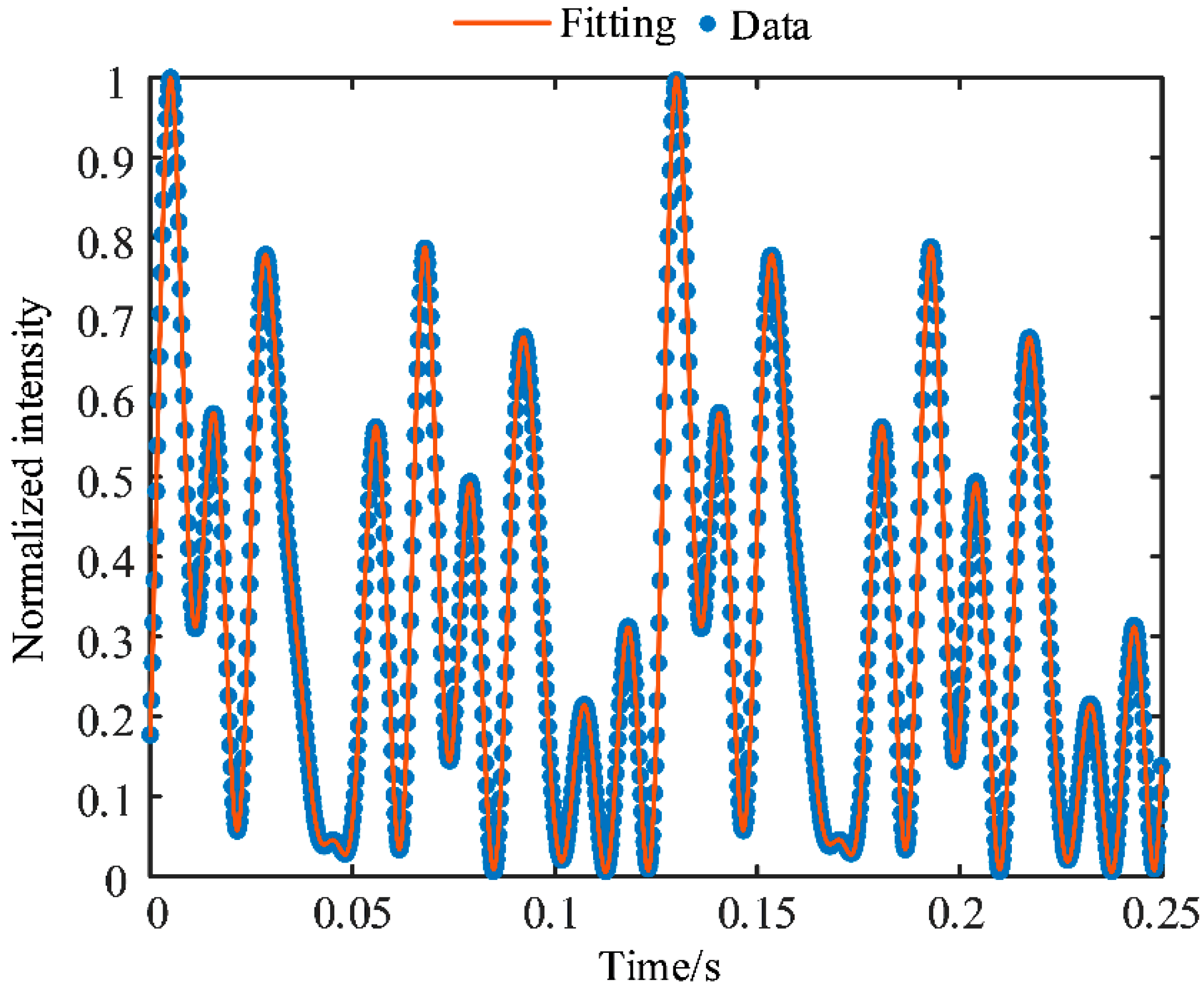
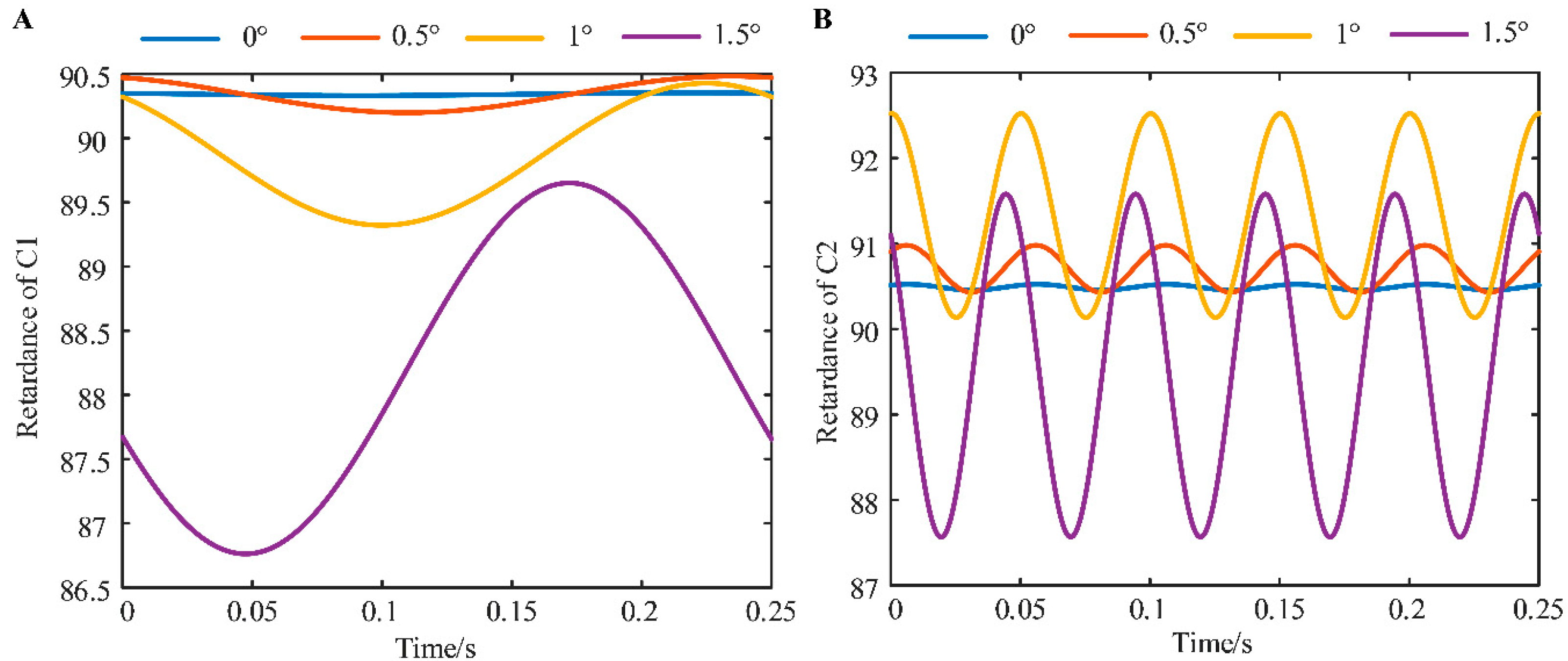
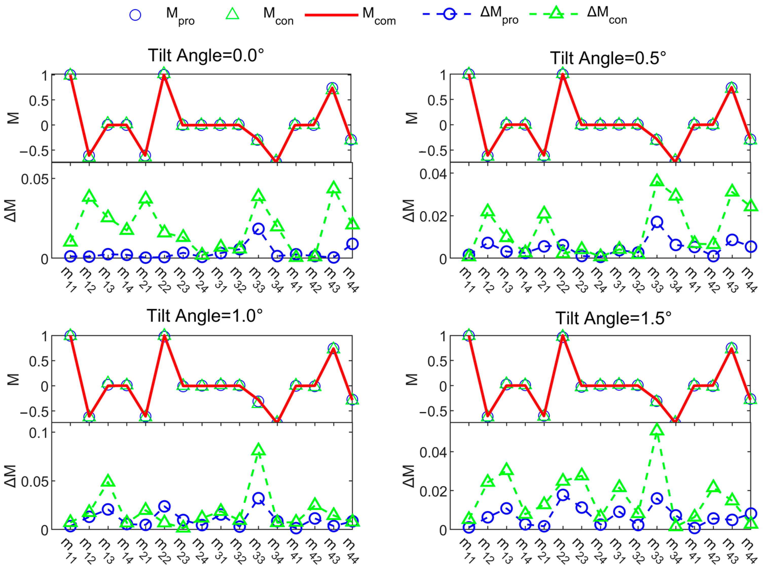
4. Experiments and Results

In this section, the validity of the characterization method was first examined through an offline experiment of the field-of-view effect. Further, the feasibility and effectiveness of the proposed characterization model was demonstrated through the measurement experiments on a set of standard SiO2 thin films with different thicknesses.
As shown in Figure 4, the method for determining the tilt angle of the beam was proposed and an offline validation experiment was carried out to ensure that the proposed method was useful. The pitching of the laser could be adjusted accurately by rotating Mirror2. A dual-size adjustable aperture and dual-reflecting mirror were introduced to ensure the accurate alignment of the laser. By adjusting the attitude angles of the reflecting mirrors to guide the laser through the small apertures, the accuracy of the alignment could be evaluated by observing the shape of the laser spot through the Cameron Beam Profiler (BC106N-VIS/M, Thorlabs, Newton, NJ, USA) (CBP). When the optical path was perfectly aligned, a small round spot on the screen of the CBP would be achieved and the position of the spot intensity peak on the screen would be nearly consistent regardless of how the CBP moved along the rail.
Then, as illustrated in Figure 5, a simple method based on a geometric principle was employed to determine the tilt angle of the beam. The relationship between the tilt angle θtilt and the spatial distance x and a was
a = x tan ( θ tilt ) ,
where a is the moving distance of the small round spot on the screen and x is the moving distance of the CBP along the rail. Therefore, we could use Mirror2 to slightly adjust the deflection angle of the laser. For example, when the moving distance x of the CBP along the rail was 25,000 μm, a 0.5° deflection angle of the laser would be obtained if the moving distance of the small round spot on the screen between Position1 and Position2 was a = x·tan (θtilt) = 218 μm. Similarly, when the movement distance of the small round spot on the screen was 436 μm and 655 μm, 1° and 1.5° deflection angles could be produced, respectively.
As shown in Figure 6, a tilt angle adjustment experiment setup on the SWE was built. Firstly, in the same way as Figure 4, a dual-size adjustable aperture and dual-reflecting mirror were introduced to ensure the accurate alignment of the laser. Moreover, a CBP was mounted onto an oblique moving stage (PHS-662C-YG, SIGMAKOKI, Sumida-ku, Tokyo, Japan), which could ensure the photosensitive screen was perpendicular to the optical axis and provided a 25,000 μm stroke along the optical axis. With the measurement configuration described above, the allowable tilt angle range of the waveplate in the instrument was 0°~1.5°. Meanwhile, according to the geometric relationship between the tilt angles θtilt1 and θtilt2 of the waveplates in the PSG and PSA shown in Figure 7, it could be assumed θtilt1θtilt2.
From Figure 7, we could find that the incident positions of the laser at different optical elements were uncertain due to the mechanical installation and adjustment errors. Therefore, it was very difficult to ensure that the laser passed through the center of the polarizers and the waveplates, which meant that more system errors would be introduced into the measurement system.
To ensure the accuracy of the standard SiO2 film thickness used for the instrument calibration, the film thicknesses were measured with a commercial spectroscopic ellipsometer (RC2 Ellipsometer, J.A. Woollam, Lincoln, NE, USA). To guarantee the measurements were carried out at the same location, a tag was attached to the center of the sample surface, whose edge was parallel to the locating edge of the sample, as shown in Figure 8. The measurements were carried out 30 times on the point next to the left edge of the tag. During the measurement, the sample was held with a vac-sorb pump installed on the sample stage to ensure no movement was introduced during the test.
During the calibration process of the instrument, the SiO2 thin film sample with a nominal thickness of 14.87 nm at a wavelength of 633 nm was used as the standard calibration sample. To demonstrate the successful application of the proposed method in the instrument parameter calibration, the comparison between the measured light intensity and the simulated light intensity at the waveplate tilt angle of 0° was chosen as an example. It could be observed from Figure 9 that the field-of-view effect of the waveplate was well characterized and the measured curves and fitting curves matched well. The results showed that the parameters and polarization effects of each component in the system were accurately calibrated.
Table 1 summarizes the system parameter calibration results at different waveplate tilt angles. The SiO2 thin film sample with a nominal thickness of 14.87 nm was used as the calibration sample. As Table 1 shows, when changing the waveplate tilt angle, the system parameters had to be recalibrated. When the calibration procedure was complete, most of the system parameters were fixed, except for ω1, ω2, C, C 2 initial , AC1, AC2, ϕC1, ϕC2 and a1. The ranges of the unfixed system parameters were determined according to the actual experiment: 1438°/s ≤ ω1 ≤ 1442°/s, 7198°/s ≤ ω2 ≤ 7202°/s, calibration value − 5° ≤ C 1 initial , C 2 initial ≤ calibration value + 5°, calibration value − 0.2 ≤ AC1, AC2 ≤ calibration value + 0.2, calibration value − 5° ≤ ϕC1, ϕC2 ≤ calibration value + 5° and 0 ≤ a1 ≤ 1.5.
The SiO2 thin film samples with nominal thicknesses of 14.87 nm, 26.62 nm, 30.70 nm, 53.84 nm and 57.04 nm were measured at different waveplate tilt angles with the SWE. Then, the field-of-view error parameters could be calculated according to Equation (21). Five sets of field-of-view error parameters could be obtained after measuring the five SiO2 thin film samples, of which we took the average. Table 2 shows that the waveplate tilt angle θtilt in the PSG was almost equal to the value set using the CBP. Moreover, it could be observed that the waveplate tilt angle θtilt in the PSG was close to the waveplate tilt angle θtilt in the PSA, and this phenomenon conformed to the prediction above. The eight field-of-view error parameters could be obtained with the proposed method. The calculated d1 and d2 in the PSG were different from d1 and d2 in the PSA. We deduced the reason to be that the incident positions of the laser at the waveplates were different, which meant that manufacture and installation errors (thickness error, optic axis tilt errors and fast axis misalignment [21]) were introduced.
The retardance fluctuation of the waveplates could be observed in Figure 10. The amplitude of the retardance fluctuation increased with the waveplate tilt angle increasing. The central retardance of the waveplates was different at different waveplate tilt angles.
To evaluate the performance of the SWE calibrated with the proposed method, we conducted measurement experiments on standard SiO2 films of varying thicknesses at different waveplate tilt angles. Since comparing the Mueller matrix results for the same sample was the most direct and reliable way to evaluate the SWE versus the commercial MME, a 57.04 nm SiO2 film was chosen as the test sample. Figure 11 summarizes the Mueller matrices measured with the different methods. The matrix elements showed good agreement between the proposed methods and with the values reported using the commercial MME. Meanwhile, the proposed method showed smaller errors in the Mueller matrix elements compared to the conventional methods. In addition, ΔMcon increased with the waveplate tilt angle, while ΔMpro did not vary with the waveplate tilt angle.
Moreover, the thicknesses of the SiO2 thin films extracted from the measured Mueller matrix at the waveplate tilt angles of 0°, 0.5°, 1° and 1.5° are summarized in Table 3. It should be noted in advance that the baseline for the thin film thickness deviation was the results reported with the commercially MME. As shown in Table 3, when the waveplate tilt angle was 0°, both the conventional method and the proposed method exhibited good performance in the thin film thickness measurement, and deviations in the thickness measurement were within 1.5%. However, the deviations in the thin film thickness obtained using the conventional method increased significantly as the waveplate tilt angle increased. In contrast, the deviations in the thin film thickness obtained with the proposed method remained stable within 1.8%, barely increasing with the rise in the waveplate tilt angle. Based on the above analysis of the measurement results, it could be concluded that the proposed calibration method could improve the accuracy and precision of the instrument and reduce the difficulty of the instrument assembly.

5. Conclusions

In this work, a waveplate characterization model and calibration method were proposed for a self-developed SWE. To compensate for the field-of-view effect in rotating waveplates with tilted incidences, we proposed a calibration method that could obtain the attitude angles of waveplates installed in the instrument and enable a decoupled extraction of all field-of-view error parameters, so that the systematic error could be evaluated reasonably. The consistency between the waveplate tilt angle from the calibrated results and offline measurement demonstrated the correctness and effectiveness of the proposed method. With the proposed method applied, the deviations in the thickness measurement on the SiO2 thin film samples were within 1.8% compared to the results reported with the commercial MME, when the waveplate tilt angle varied as much as 0°, 0.5°, 1° or 1.5°. The proposed calibration method could not only improve the accuracy and precision of the instrument, but also provide theoretical guidance for the installation and commissioning of the relevant optical systems.

Author Contributions

Conceptualization, Z.J., S.Z. and H.J.; methodology, Z.J., S.Z. and H.J.; software, Z.J. and S.Z.; validation, Z.J. and S.Z.; formal analysis, Z.J. and S.Z.; investigation, Z.J. and S.Z.; resources, S.L. and H.J.; data curation, Z.J. and S.Z.; writing—original draft preparation, Z.J. and S.Z.; writing—review and editing, Z.J., S.Z., H.J. and S.L.; visualization, Z.J. and S.Z.; supervision, S.L. and H.J.; project administration, S.L. and H.J.; funding acquisition, S.L. and H.J. All authors have read and agreed to the published version of the manuscript.

Funding

This work was funded by the National Natural Science Foundation of China (51975232 and 52205592) and the National Key Research and Development Plan (grant no. 2017YFF0204705).

Institutional Review Board Statement

Not applicable.

Informed Consent Statement

Not applicable.

Data Availability Statement

Not applicable.

Conflicts of Interest

The authors declare no conflict of interest.

References

  1. Lee, S.H.; Kim, M.Y.; Ser, J.-I.; Park, J. Asymmetric polarization-based frequency scanning interferometer. Opt. Express 2015, 23, 7333–7344. [Google Scholar] [CrossRef]
  2. Liu, L.; Zeng, A.; Zhu, L.; Huang, H. Lateral shearing interferometer with variable shearing for measurement of a small beam. Opt. Lett. 2014, 39, 1992–1995. [Google Scholar] [CrossRef]
  3. Sato, T.; Araki, T.; Sasaki, Y.; Tsuru, T.; Tadokoro, T.; Kawakami, S. Compact ellipsometer employing a static polarimeter module with arrayed polarizer and wave-plate elements. Appl. Opt. 2007, 46, 4963–4967. [Google Scholar] [CrossRef] [PubMed]
  4. Aspnes, D.E. Spectroscopic ellipsometry—Past, present, and future. Thin Solid Films 2014, 571, 334–344. [Google Scholar] [CrossRef]
  5. Aas, L.M.S.; Ellingsen, P.G.; Fladmark, B.E.; Letnes, P.A.; Kildemo, M. Overdetermined broadband spectroscopic Mueller matrix polarimeter designed by genetic algorithms. Opt. Express 2013, 2021, 8753–8762. [Google Scholar] [CrossRef] [PubMed]
  6. De Martino, A.; Kim, Y.-K.; Garcia-Caurel, E.; Laude, B.; Drévillon, B. Optimized Mueller polarimeter with liquid crystals. Opt. Lett. 2003, 28, 616–618. [Google Scholar] [CrossRef]
  7. Williams, P.A. Rotating-wave-plate Stokes polarimeter for differential group delay measurements of polarization-mode dispersion. Appl. Opt. 1999, 38, 6508–6515. [Google Scholar] [CrossRef]
  8. Aspnes, D.E.; Studna, A.A. High Precision Scanning Ellipsometer. Appl. Opt. 1975, 14, 220–228. [Google Scholar] [CrossRef]
  9. Azzam, R.M.A. Photopolarimetric measurement of the Mueller matrix by Fourier analysis of a single detected signal. Opt. Lett. 1978, 2, 148–150. [Google Scholar] [CrossRef]
  10. Sun, C.; Ye, S.; Jian, S. Solc-Like Tunable Birefringent Fiber Filter Based on Elliptical-Core Spun Fiber. IEEE Photonics Technol. Lett. 2017, 29, 1031–1034. [Google Scholar] [CrossRef]
  11. Demirbas, U.; Uecker, R.; Fujimoto, J.G.; Leitenstorfer, A. Multicolor lasers using birefringent filters: Experimental demonstration with Cr:Nd:GSGG and Cr:LiSAF. Opt. Express 2017, 25, 2594–2607. [Google Scholar] [CrossRef] [PubMed]
  12. Hagen, N.; Yoshida, K.; Shan, Y.; Otani, Y. Apophyllite waveplates. Appl. Opt. 2022, 61, 6518–6526. [Google Scholar] [CrossRef] [PubMed]
  13. Emam-Ismail, M. Experimental realization of short-wavelength infrared half wave retarder fabricated from ZnO single crystal plates. Opt. Mater. 2023, 135, 113297. [Google Scholar] [CrossRef]
  14. Emam-Ismail, M. Wide spectral range multiple orders and half-wave achromatic phase retarders fabricated from two lithium tantalite single crystal plates. Opt. Laser Technol. 2015, 74, 108–118. [Google Scholar] [CrossRef]
  15. Emam-Ismail, M. Experimental realization of multi, zero, dual order and achromatic gypsum wave plate in a wavelength range 400–1000 nm. Opt. Commun. 2013, 292, 18–24. [Google Scholar] [CrossRef]
  16. Boulbry, B.; Bousquet, B.; Jeune, B.L.; Guern, Y.; Lotrian, J. Polarization errors associated with zero-order achromatic quarter-wave plates in the whole visible spectral range. Opt. Express 2001, 9, 225–235. [Google Scholar] [CrossRef]
  17. Dai, H.; Yan, C. Measurement errors resulted from misalignment errors of the retarder in a rotating-retarder complete Stokes polarimeter. Opt. Express 2014, 22, 11869–11883. [Google Scholar] [CrossRef]
  18. Dong, H.; Tang, M.; Gong, Y. Measurement errors induced by deformation of optical axes of achromatic waveplate retarders in RRFP Stokes polarimeters. Opt. Express 2012, 20, 26649–26666. [Google Scholar] [CrossRef]
  19. Lee, J.; Rovira, P.I.; An, I.; Collins, R.W. Alignment and calibration of the MgF2 biplate compensator for applications in rotating-compensator multichannel ellipsometry. J. Opt. Soc. Am. A 2001, 18, 1980–1985. [Google Scholar] [CrossRef]
  20. Zhang, S.; Jiang, H.; Gu, H.; Chen, X.; Liu, S. Attitude metrology based on the field-of-view effect of birefringence using high-speed polarimetry. Opt. Lett. 2020, 45, 2074–2077. [Google Scholar] [CrossRef]
  21. Gu, H.; Chen, X.; Zhang, C.; Jiang, H.; Liu, S. Study of the retardance of a birefringent waveplate at tilt incidence by Mueller matrix ellipsometer. J. Opt. 2018, 20, 015401. [Google Scholar] [CrossRef]
  22. Hsieh, C.H.; Tsai, C.C.; Wei, H.C.; Yu, L.P.; Wu, J.S.; Chou, C. Determination of retardation parameters of multiple-order wave plate using a phase-sensitive heterodyne ellipsometer. Appl. Opt. 2007, 46, 5944–5950. [Google Scholar] [CrossRef] [PubMed]
  23. Arteaga, O.; Canillas, A.; Jellison, G.E., Jr. Determination of the components of the gyration tensor of quartz by oblique incidence transmission two-modulator generalized ellipsometry. Appl. Opt. 2009, 48, 5307–5317. [Google Scholar] [CrossRef] [PubMed]
  24. West, E.A.; Smith, M.H. Polarization errors associated with birefringent waveplates. Opt. Eng. 1995, 2265, 1574–1580. [Google Scholar] [CrossRef]
  25. Ruder, A.; Wright, B.; Peev, D.; Feder, R.; Kilic, U.; Hilfiker, M.; Schubert, E.; Herzinger, C.M.; Schubert, M. Mueller matrix ellipsometer using dual continuously rotating anisotropic mirrors. Opt. Lett. 2020, 45, 3541–3544. [Google Scholar] [CrossRef]
  26. Fujiwara, H. Spectroscopic Ellipsometry: Principles and Applications; John Wiley & Sons: Chichester, UK, 2007; pp. 52–59. [Google Scholar]
  27. Liao, C.C.; Lo, Y.L. Extraction of anisotropic parameters of turbid media using hybrid model comprising differential-and decomposition-based Mueller matrices. Opt. Express 2013, 21, 16831–16853. [Google Scholar] [CrossRef]
  28. Veiras, F.E.; Perez, L.I.; Garea, M.T. Phase shift formulas in uniaxial media: An application to waveplates. Appl. Opt. 2010, 49, 2769–2777. [Google Scholar] [CrossRef]
  29. Avendaño-Alejo, M.; Rosete-Aguilar, M. Optical path difference in a plane-parallel uniaxial plate. J. Opt. Soc. Am. A 2006, 234, 926–932. [Google Scholar] [CrossRef]
  30. Bass, M.; Van Stryland, E.W.; Williams, D.R.; Wolfe, W.L. Handbook of Optics; McGraw-Hill: New York, NY, USA, 1995; pp. 15.1–15.100. [Google Scholar]
  31. Pezzaniti, J.L.; Chipman, R.A. Angular dependence of polarizing beam-splitter cubes. Appl. Opt. 1994, 33, 1916–1929. [Google Scholar] [CrossRef]
  32. Lo, Y.-L.; Pham, T.-T.-H.; Chen, P.-C. Characterization on five effective parameters of anisotropic optical material using Stokes parameters—Demonstration by a fiber-type polarimeter. Opt. Express 2010, 18, 9133–9150. [Google Scholar] [CrossRef]
  33. El-Agez, T.M.; Taya, S.A. Development and construction of rotating polarizer analyzer ellipsometer. Opt. Lasers Eng. 2011, 49, 507–513. [Google Scholar] [CrossRef]
  34. Argenti, F.; Torricelli, G.; Alparone, L. MMSE filtering of generalised signal-dependent noise in spatial and shift-invariant wavelet domains. Signal Process. 2006, 86, 2056–2066. [Google Scholar] [CrossRef]
  35. Novikova, T.; Bulkin, P. Inverse problem of Mueller polarimetry for metrological applications. J. Inverse Ill-Posed Probl. 2021, 29, 759–774. [Google Scholar] [CrossRef]
Figure 1. (A) Schematic of the wave normal propagation in a waveplate under an arbitrary incidence and an arbitrary azimuth of the incident light. (B) Refractive index of quartz.
Photonics 10 01038 g001
Figure 2. Retardance oscillations versus the azimuth at different waveplate tilt angles.
Photonics 10 01038 g002
Figure 3. Critical components and beam path of the SWE. The ellipsometer was composed of a He–Ne laser light source (laser), an optical isolator (IO), a beam splitter (BS), two detectors (detector1 and detector2), a narrowband filter (FB), a beam expander (BE) (GBE-03A, Thorlabs, Newton, NJ, USA), six apertures (AP1–AP6) (SM1D12CZ, Thorlabs, Newton, NJ, USA), two mirrors (M1, M2), two polarizers (P1 and P2) (LPVISC100-MP2, Thorlabs, Newton, NJ, USA), two continuously rotating waveplates (WP1 and WP2) (WPQ10M-633, Thorlabs, Newton, NJ, USA) and two focus lens (L1 and L2). Incident and reflected beams are denoted in red.
Photonics 10 01038 g003
Figure 4. An offline validation experiment to measure the deflection angle of a beam: (A) schematic diagram; (B) experiment setup.
Photonics 10 01038 g004
Figure 5. Geometric principles of the determination of the deflection angle of the beam.
Photonics 10 01038 g005
Figure 6. A deflection angle adjustment experiment: (A) schematic diagram; (B) experiment setup.
Photonics 10 01038 g006
Figure 7. Schematic of the laser propagation in the constructed SWE and the field-of-view effect.
Photonics 10 01038 g007
Figure 8. The diagram of the point positioning. (A) The silicon wafer; (B) area of measurement.
Photonics 10 01038 g008
Figure 9. Measured and fitting results of the SiO2 thin film sample with thickness of 14.87 nm at the wavelength of 633 nm, the instrument incident angle of 65° and the waveplate tilt angle of 0°.
Photonics 10 01038 g009
Figure 10. Retardance oscillation calibration results versus the time (the azimuth) at different waveplate tilt angles: (A) PSG; (B)PSA.
Photonics 10 01038 g010
Figure 11. Mueller matrix comparison of SiO2 thin films with thickness of 57.04 nm at different waveplate tilt angles; Mpro represent the Mueller matrix measured with the proposed method, Mcon represents the Mueller matrix measured with the conventional method and Mcom represents the Mueller matrix measured with the commercial MME; ΔMpro represents the absolute value of the difference between Mpro and Mcom, while ΔMcon represents the absolute value of the difference between Mcon and Mcom.
Photonics 10 01038 g011
Table 1. System parameters extracted from the calibration of waveplates at different waveplate tilt angles.
Tilt Angle (°)
(Absolute Value)
System ParametersSystem ParametersSystem Parameters
0P (°)33.530ω2 (°/s)7200.006b20.012
A (°)28.650AC1−0.011c20.003
Dt10.995AC20.034θincident (°)64.944
Dt20.989ϕC1 (°/s)−42.173a0−0.003
δP (°)0ϕC2 (°/s)42.717a11.010
δA (°)0 δ C 1 center (°/s)90.343a2−0.037
C 1 initial (°)−41.663 δ C 2 center (°/s)90.490a30.029
C 2 initial (°)−62.177b1−0.001
ω1 (°/s)1440.136c1−0.005
0.5P (°)33.561ω2 (°/s)7200.059b20.010
A (°)28.547AC1−0.142c20.003
Dt10.995AC20.275θincident (°)64.944
Dt20.989ϕC1 (°/s)−68.006a0−0.003
δP (°)0ϕC2 (°/s)46.404a11.012
δA (°)0 δ C 1 center (°/s)90.341a2−0.037
C 1 initial (°)−41.829 δ C 2 center (°/s)90.706a30.029
C 2 initial (°)−63.398b1−0.005
ω1 (°/s)1440.382c1−0.003
1P (°)33.655ω2 (°/s)7200.350b20.019
A (°)28.238AC1−0.553c20.003
Dt10.990AC2−1.193θincident (°)65.360
Dt20.989ϕC1 (°/s)−53.970a0−0.003
δP (°)0ϕC2 (°/s)−91.971a11.004
δA (°)0 δ C 1 center (°/s)89.875a2−0.037
C 1 initial (°)−41.474 δ C 2 center (°/s)91.329a30.029
C 2 initial (°)−62.944b10.006
ω1 (°/s)1441.193c1−0.018
1.5P (°)33.806ω2 (°/s)7199.663b20.051
A (°)27.392AC1−1.445c2−0.016
Dt10.987AC2−2.006θincident (°)65.111
Dt20.989ϕC1 (°/s)21.634a0−0.003
δP (°)0ϕC2 (°/s)−49.868a10.994
δA (°)0 δ C 1 center (°/s)88.207a2−0.037
C 1 initial (°)−25.577 δ C 2 center (°/s)89.573a30.029
C 2 initial (°)−67.841b10.007
ω1 (°/s)1441.522c1−0.025
Table 2. Parameters of field-of-view effect extracted from the calibration of waveplates at different waveplate tilt angles.
Tilt Angle (°)
(Absolute Value)
Field-of-View Error Parameters
PSGPSA
θtilt (°)β (°)d1 (μm)d2 (μm)θtilt (°)β (°)d1 (μm)d2 (μm)
0−0.111−66.074995.912978.363−0.23266.368980.360962.783
0.5−0.465101.020995.913978.365−0.65568.215980.348962.728
1−0.924108.080995.798978.340−1.35989.045991.744974.004
1.5−1.491−33.977996.408979.274−1.756109.951998.445981.046
Table 3. Thickness measurement results of the five SiO2 samples at different waveplate tilt angles.
Tilt
Angle (°)
Silicon DioxideRC2 d (nm)Conventional MethodDeviationProposed MethodDeviation
d (nm)|Δ (nm)|d (nm)|Δ (nm)|
Sample114.9714.750.221.470%14.750.220.1470%
Sample225.3825.420.040.158%25.380.000.000%
Sample330.3330.070.260.857%30.050.280.890%
Sample453.0152.480.531.000%52.440.571.075%
Sample557.0456.620.420.736%56.560.480.842%
0.5°Sample114.9714.940.030.200%14.950.020.134%
Sample225.3824.660.722.837%25.330.050.197%
Sample330.3329.061.274.187%30.010.321.055%
Sample453.0149.923.095.829%52.220.791.490%
Sample557.0453.733.315.803%56.270.771.350%
1.0°Sample114.9715.060.090.601%15.080.110.735%
Sample225.3826.491.114.622%25.740.361.418%
Sample330.3330.980.652.143%29.950.381.253%
Sample453.0151.151.863.509%53.570.561.056%
Sample557.0455.012.033.559%57.680.631.104%
1.5°Sample114.9716.011.046.496%15.110.140.935%
Sample225.3825.530.150.59%25.780.401.576%
Sample330.3329.780.551.813%30.260.070.231%
Sample453.0150.542.464.641%52.110.901.698%
Sample557.0454.322.724.769%56.060.981.718%
Disclaimer/Publisher’s Note: The statements, opinions and data contained in all publications are solely those of the individual author(s) and contributor(s) and not of MDPI and/or the editor(s). MDPI and/or the editor(s) disclaim responsibility for any injury to people or property resulting from any ideas, methods, instructions or products referred to in the content.

